Chapter 18 NONIDEAL MOS Sung June Kim kimsjsnu

- Slides: 24

Chapter 18. NONIDEAL MOS Sung June Kim kimsj@snu. ac. kr http: //nanobio. snu. ac. kr NONIDEAL MOS

CONTENTS · · · Metal-Semiconductor Work function Difference Oxide Charges MOSFET Threshold Considerations NONIDEAL MOS

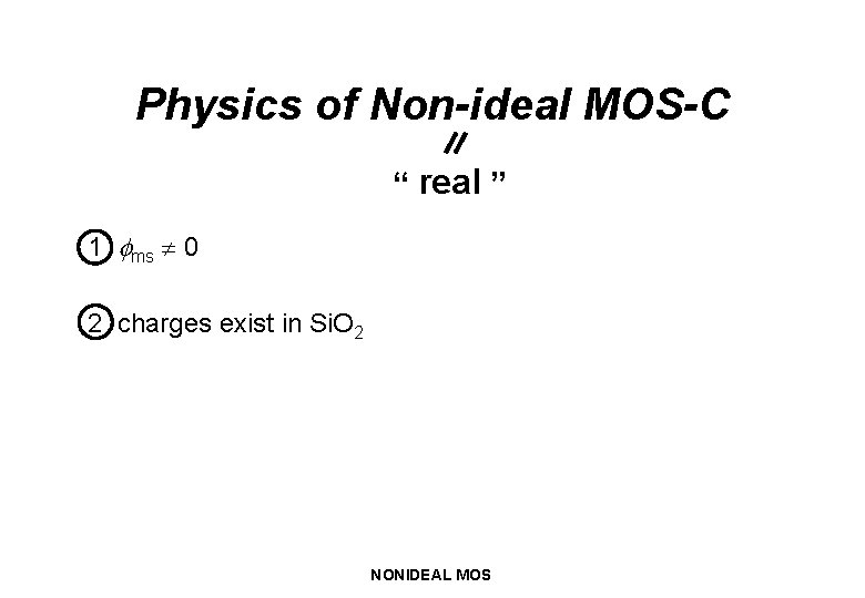
Physics of Non-ideal MOS-C “ real ” 1 ms 0 2 charges exist in Si. O 2 NONIDEAL MOS

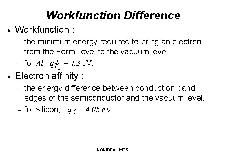
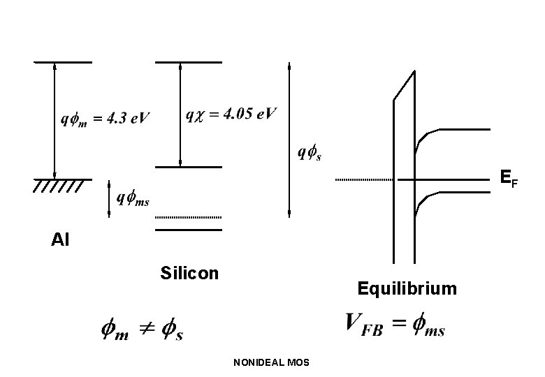
Workfunction Difference · Workfunction : - · the minimum energy required to bring an electron from the Fermi level to the vacuum level. for Al, q m = 4. 3 e. V. Electron affinity : - the energy difference between conduction band edges of the semiconductor and the vacuum level. for silicon, q = 4. 05 e. V. NONIDEAL MOS

EF Al Silicon Equilibrium NONIDEAL MOS

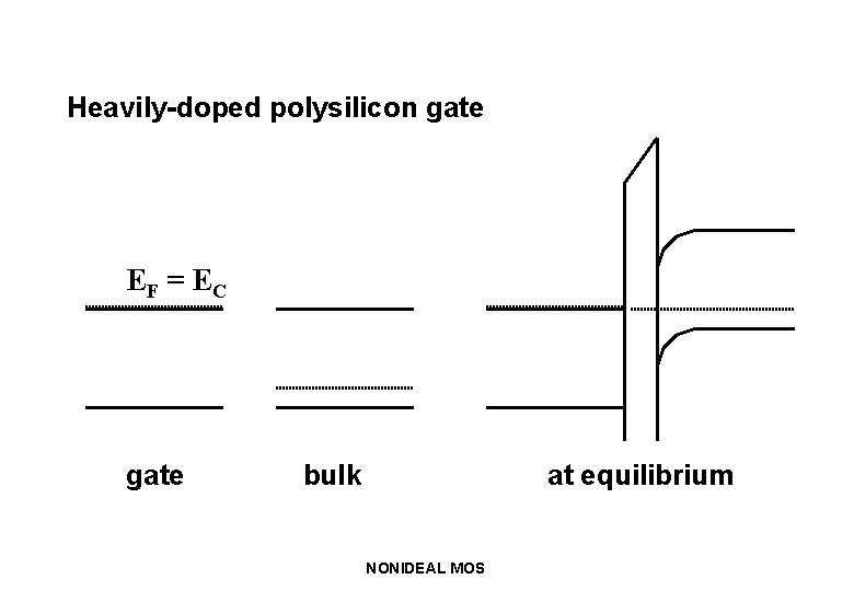
Heavily-doped polysilicon gate EF = E C gate bulk at equilibrium NONIDEAL MOS

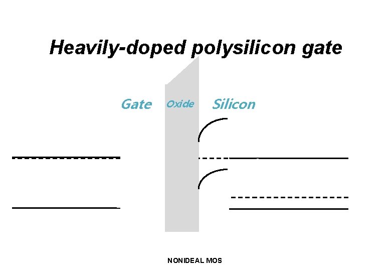
Heavily-doped polysilicon gate Gate Oxide Silicon NONIDEAL MOS

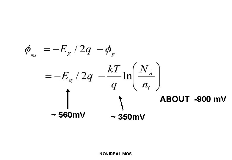
ABOUT -900 m. V ~ 560 m. V ~ 350 m. V NONIDEAL MOS

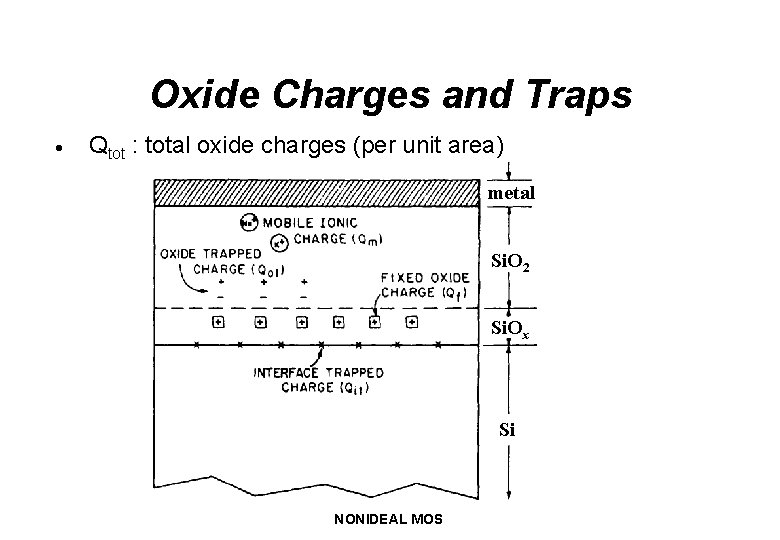
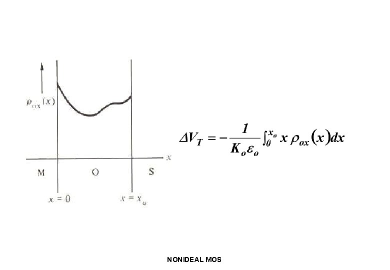
Oxide Charges and Traps · Qtot : total oxide charges (per unit area) metal Si. O 2 Si. Ox Si NONIDEAL MOS

NONIDEAL MOS

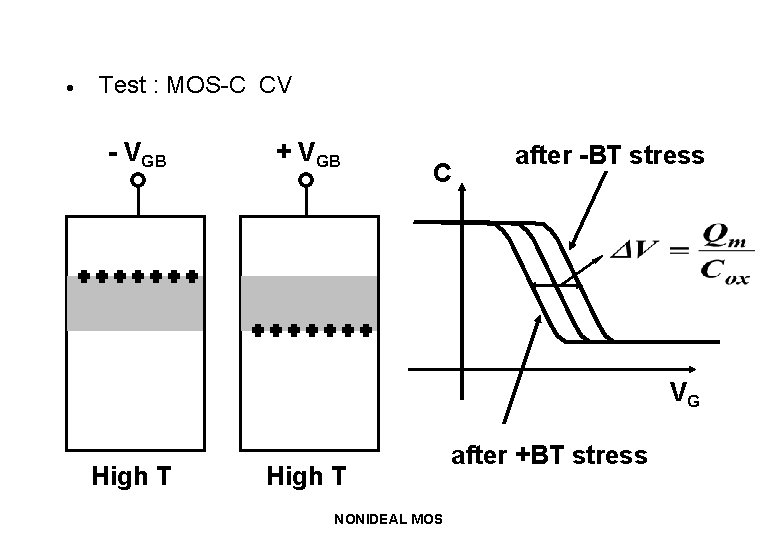
Mobile Ionic Charges · · Na+, K+ Very high diffusivities in the oxide even below 200 C - VT instability NONIDEAL MOS

· Test : MOS-C CV - VGB + VGB C after -BT stress VG High T NONIDEAL MOS after +BT stress

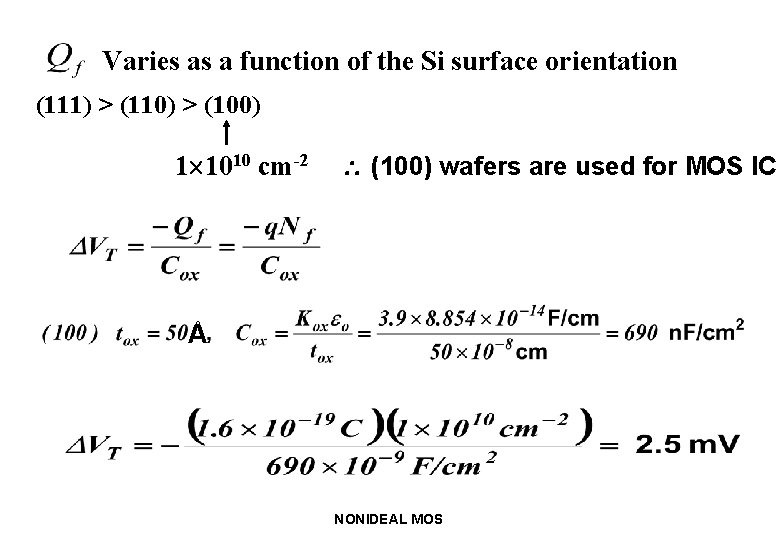
Fixed Oxide Charge 1. Located very close to the interface 2. Associated with the structure of the interfacial between Si and Si. O 2 3. Function of substrate orientation, oxidation temperature (annealing condition) NONIDEAL MOS

Varies as a function of the Si surface orientation (111) > (110) > (100) 1 1010 cm-2 (100) wafers are used for MOS IC Å NONIDEAL MOS

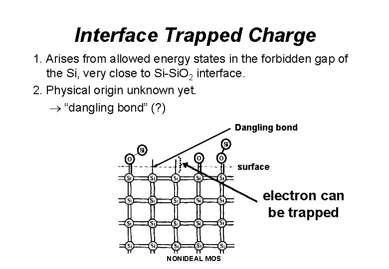
Interface Trapped Charge 1. Arises from allowed energy states in the forbidden gap of the Si, very close to Si-Si. O 2 interface. 2. Physical origin unknown yet. “dangling bond” (? ) Dangling bond Si Si O O O surface electron can be trapped NONIDEAL MOS

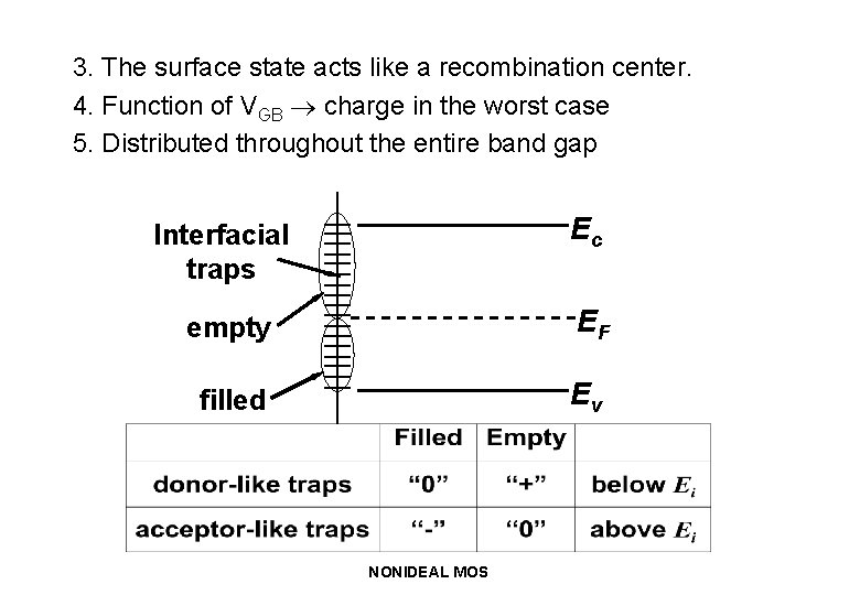
3. The surface state acts like a recombination center. 4. Function of VGB charge in the worst case 5. Distributed throughout the entire band gap Interfacial traps Ec empty EF filled Ev NONIDEAL MOS

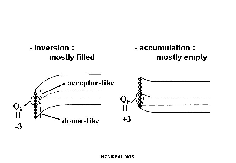
- inversion : mostly filled - accumulation : mostly empty acceptor-like Qit -3 donor-like +3 NONIDEAL MOS

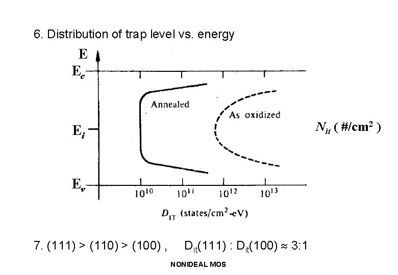
6. Distribution of trap level vs. energy E Ec Nit ( #/cm 2 ) Ei Ev 7. (111) > (110) > (100) , Dit(111) : Dit(100) 3: 1 NONIDEAL MOS

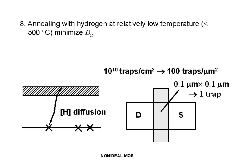
8. Annealing with hydrogen at relatively low temperature ( 500 C) minimize Dit. 1010 traps/cm 2 100 traps/ m 2 0. 1 m 1 trap [H] diffusion NONIDEAL MOS D S

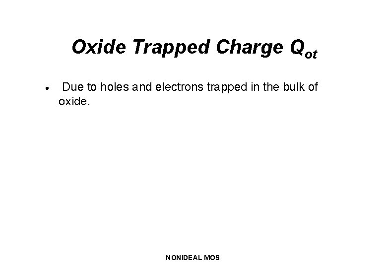
Oxide Trapped Charge Qot · Due to holes and electrons trapped in the bulk of oxide. NONIDEAL MOS

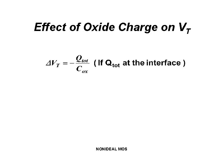
Effect of Oxide Charge on VT NONIDEAL MOS

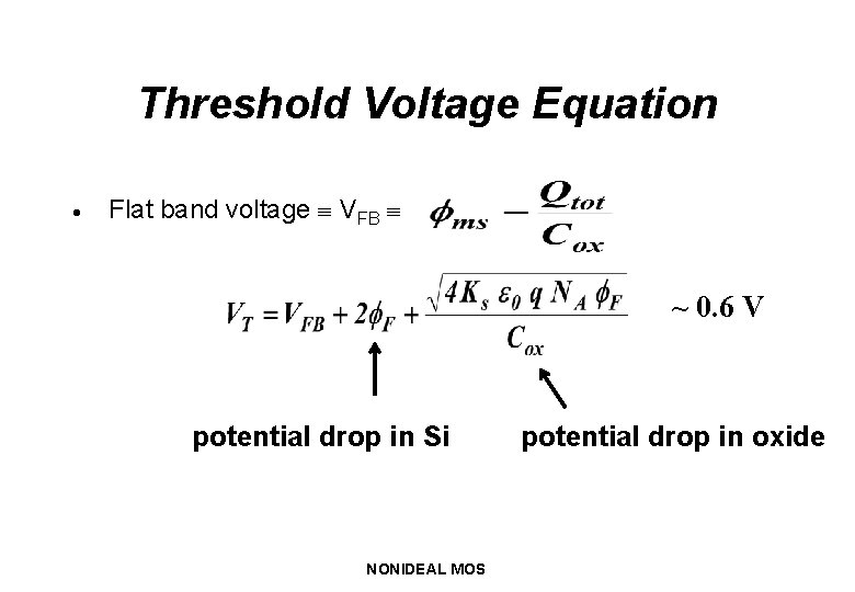
Threshold Voltage Equation · Flat band voltage VFB ~ 0. 6 V potential drop in Si NONIDEAL MOS potential drop in oxide

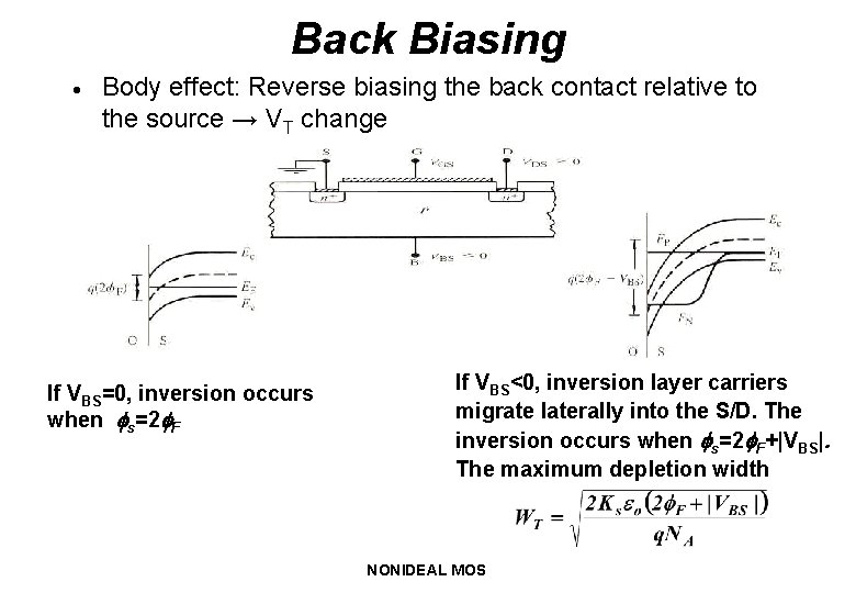
Back Biasing · Body effect: Reverse biasing the back contact relative to the source → VT change If VBS=0, inversion occurs when s=2 F If VBS<0, inversion layer carriers migrate laterally into the S/D. The inversion occurs when s=2 F+|VBS|. The maximum depletion width NONIDEAL MOS

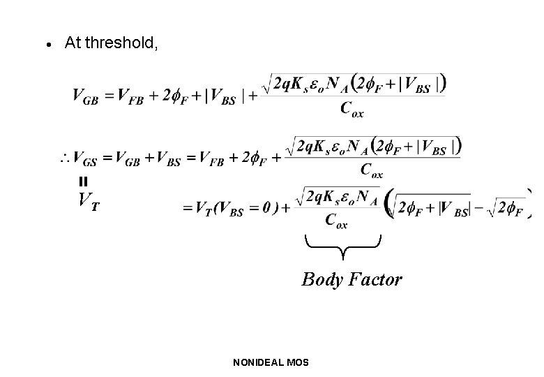
· At threshold, = VT Body Factor NONIDEAL MOS