Chapter 17 MOSFETs An Introduction Sung June Kim

- Slides: 30

Chapter 17. MOSFETs - An Introduction Sung June Kim kimsj@snu. ac. kr http: //nanobio. snu. ac. kr MOSFETs – An Introduction

CONTENTS · Qualitative Theory of Operation · Quantitative I - V Relationships · Subthreshold Swing · ac Response D D MOSFETs – An Introduction

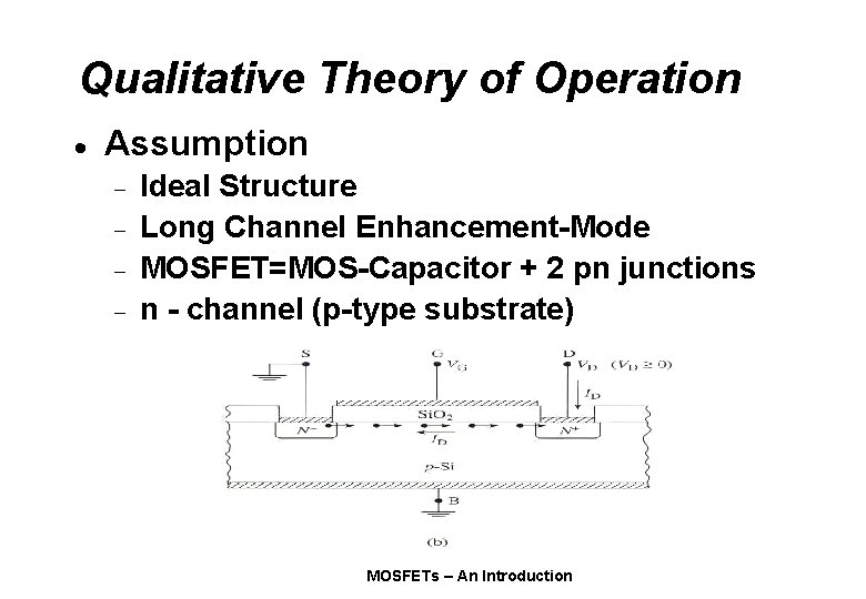
Qualitative Theory of Operation · Assumption - Ideal Structure Long Channel Enhancement-Mode MOSFET=MOS-Capacitor + 2 pn junctions n - channel (p-type substrate) MOSFETs – An Introduction

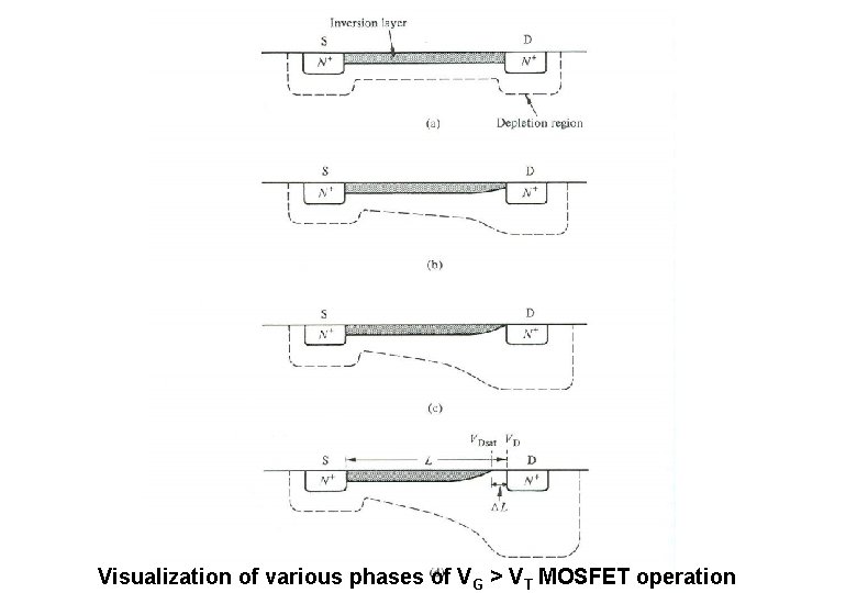
MOSFETs – An Introduction Visualization of various phases of VG > VT MOSFET operation

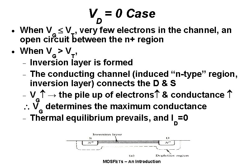
VD = 0 Case · · When VG VT, very few electrons in the channel, an open circuit between the n+ region When VG > VT, - Inversion layer is formed - The conducting channel (induced “n-type” region, inversion layer) connects the D & S - V → the pile up of electrons & conductance G VG determines the maximum conductance - Thermal equilibrium prevails, and I =0 D MOSFETs – An Introduction

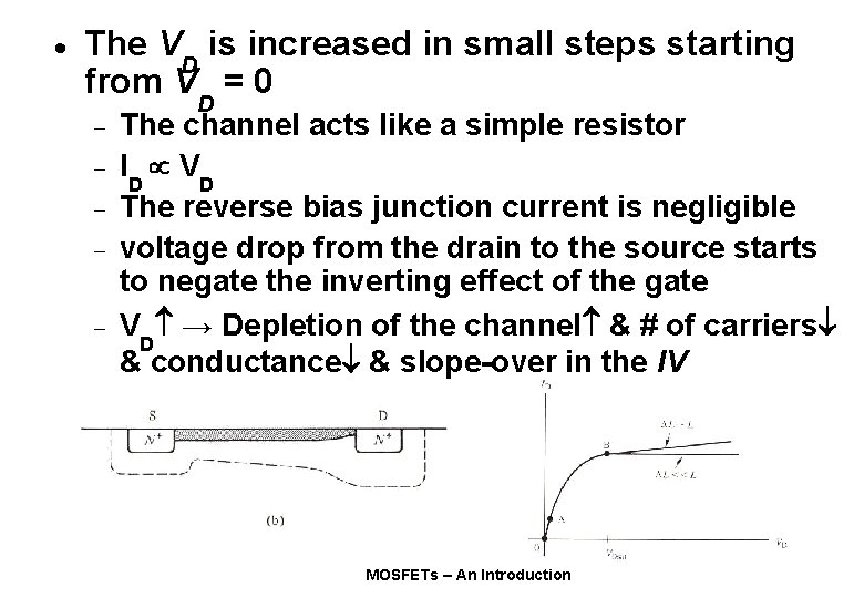
· The V is increased in small steps starting D from V = 0 - D The channel acts like a simple resistor I V D D The reverse bias junction current is negligible voltage drop from the drain to the source starts to negate the inverting effect of the gate V → Depletion of the channel & # of carriers D & conductance & slope-over in the IV MOSFETs – An Introduction

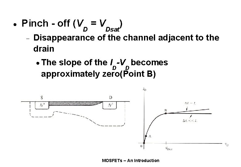
· Pinch - off (V = V D - Dsat ) Disappearance of the channel adjacent to the drain · The slope of the I -V becomes D D approximately zero(Point B) MOSFETs – An Introduction

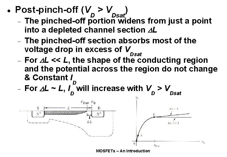
· Post-pinch-off (V > V - - D Dsat ) The pinched-off portion widens from just a point into a depleted channel section L The pinched-off section absorbs most of the voltage drop in excess of VDsat For L << L, the shape of the conducting region and the potential across the region do not change & Constant I D For L ~ L, I will increase with VD > VDsat D MOSFETs – An Introduction

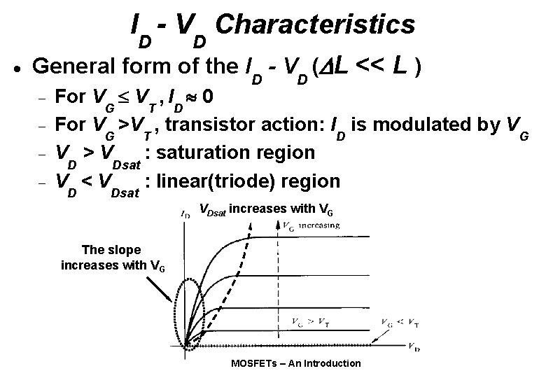
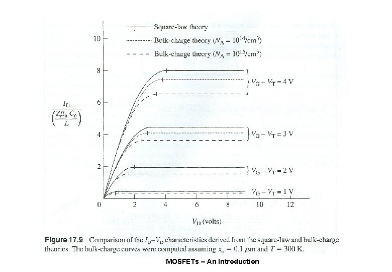
I - V Characteristics D · D General form of the I - V ( L << L ) - D D For VG VT , I 0 D For VG >VT , transistor action: ID is modulated by VG V >V : saturation region D Dsat V <V : linear(triode) region D Dsat VDsat increases with VG The slope increases with VG MOSFETs – An Introduction

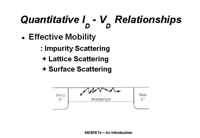
Quantitative I - V Relationships D · D Effective Mobility : Impurity Scattering + Lattice Scattering + Surface Scattering MOSFETs – An Introduction

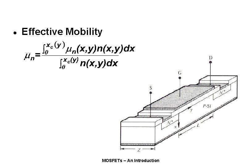
· Effective Mobility MOSFETs – An Introduction

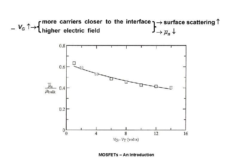
– MOSFETs – An Introduction

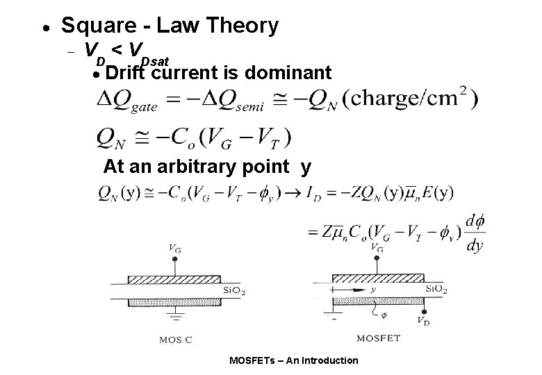
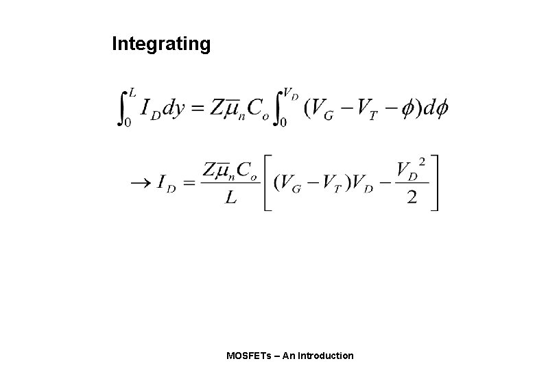
· Square - Law Theory - V <V D Dsat · Drift current is dominant At an arbitrary point y MOSFETs – An Introduction

Integrating MOSFETs – An Introduction

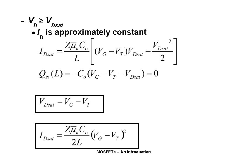
- V V D Dsat · I is approximately constant D MOSFETs – An Introduction

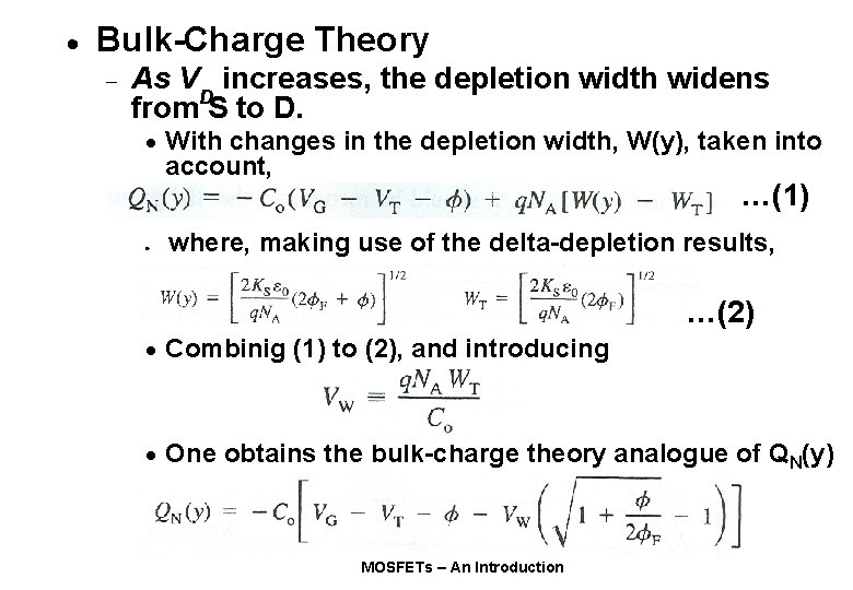
· Bulk-Charge Theory - As V increases, the depletion width widens from. DS to D. · With changes in the depletion width, W(y), taken into account, · …(1) where, making use of the delta-depletion results, …(2) · Combinig (1) to (2), and introducing · One obtains the bulk-charge theory analogue of QN(y) MOSFETs – An Introduction

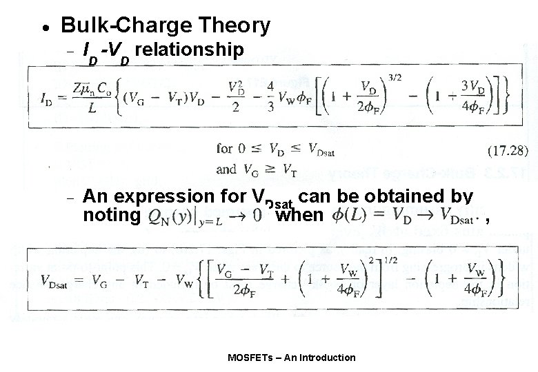
· Bulk-Charge Theory - I -V relationship - An expression for VDsat can be obtained by noting when , D D MOSFETs – An Introduction

MOSFETs – An Introduction

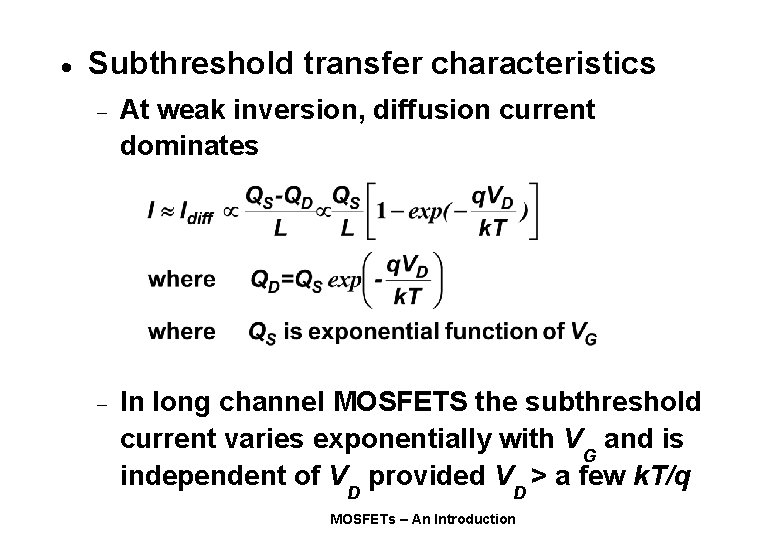
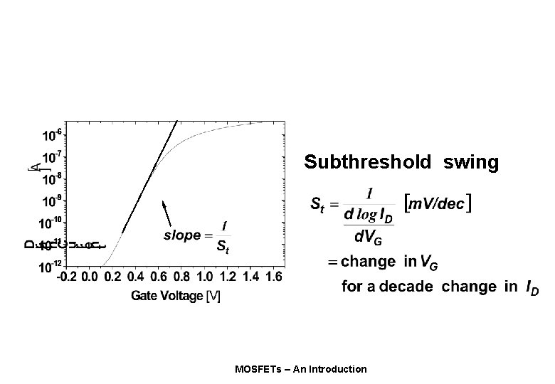
· Subthreshold transfer characteristics - At weak inversion, diffusion current dominates - In long channel MOSFETS the subthreshold current varies exponentially with VG and is independent of VD provided VD > a few k. T/q MOSFETs – An Introduction

Subthreshold swing MOSFETs – An Introduction

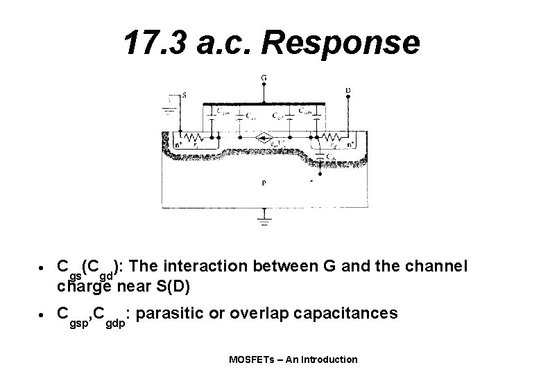
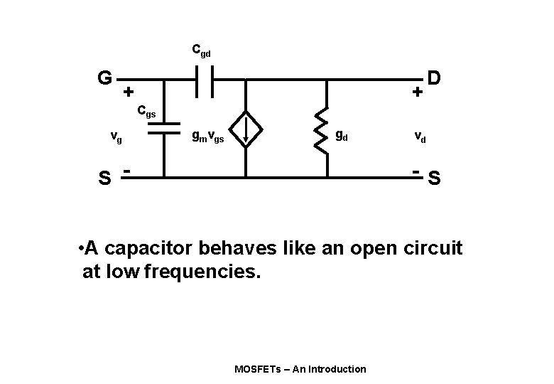
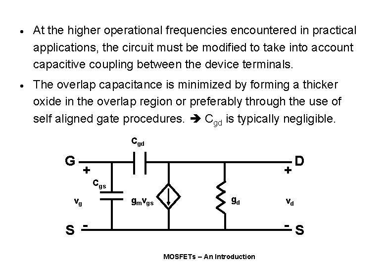
17. 3 a. c. Response · Cgs(Cgd): The interaction between G and the channel charge near S(D) · Cgsp, Cgdp: parasitic or overlap capacitances MOSFETs – An Introduction

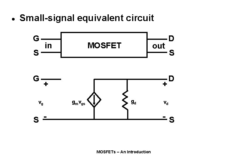
· Small-signal equivalent circuit G S G in MOSFET out + vg + gmvgs gd S - D S D vd - S MOSFETs – An Introduction

Cgd G + vg + Cgs gmvgs gd S - D vd - S • A capacitor behaves like an open circuit at low frequencies. MOSFETs – An Introduction

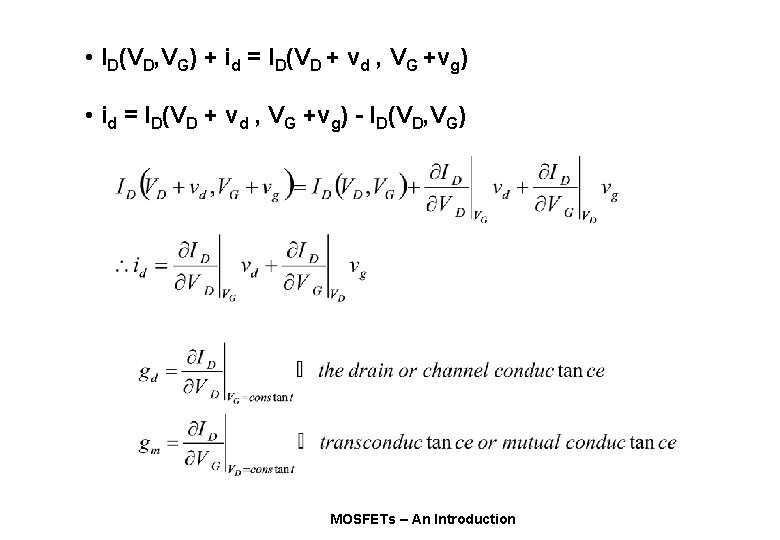
• ID(VD, VG) + id = ID(VD + vd , VG +vg) • id = ID(VD + vd , VG +vg) - ID(VD, VG) MOSFETs – An Introduction

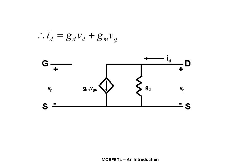
G id + vg + gmvgs gd S - D vd - S MOSFETs – An Introduction

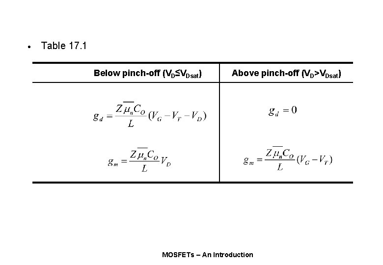
· Table 17. 1 Below pinch-off (VD≤VDsat) Above pinch-off (VD>VDsat) MOSFETs – An Introduction

· At the higher operational frequencies encountered in practical applications, the circuit must be modified to take into account capacitive coupling between the device terminals. · The overlap capacitance is minimized by forming a thicker oxide in the overlap region or preferably through the use of self aligned gate procedures. Cgd is typically negligible. Cgd G + vg + Cgs gmvgs gd S - D vd - S MOSFETs – An Introduction

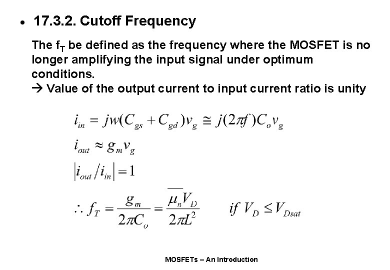
· 17. 3. 2. Cutoff Frequency The f. T be defined as the frequency where the MOSFET is no longer amplifying the input signal under optimum conditions. Value of the output current to input current ratio is unity MOSFETs – An Introduction

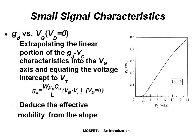
Small Signal Characteristics · gd vs. VG(VD=0) - - Extrapolating the linear portion of the gd-VG characteristics into the VG axis and equating the voltage intercept to VT Deduce the effective mobility from the slope MOSFETs – An Introduction

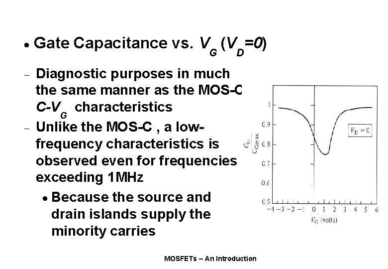
· Gate Capacitance vs. VG (VD=0) - Diagnostic purposes in much the same manner as the MOS-C C-VG characteristics Unlike the MOS-C , a lowfrequency characteristics is observed even for frequencies exceeding 1 MHz · Because the source and drain islands supply the minority carries - MOSFETs – An Introduction