Chapter 17 Electronics Fundamentals Circuits Devices and Applications


- Slides: 13

Chapter 17 Electronics Fundamentals Circuits, Devices and Applications - Floyd © Copyright 2007 Prentice-Hall

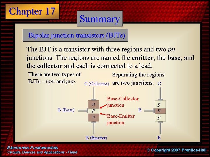
Chapter 17 Summary Bipolar junction transistors (BJTs) The BJT is a transistor with three regions and two pn junctions. The regions are named the emitter, the base, and the collector and each is connected to a lead. There are two types of BJTs – npn and pnp. B (Base) C (Collector) n p n Base-Collector junction Base-Emitter junction E (Emitter) Electronics Fundamentals Circuits, Devices and Applications - Floyd Separating the regions are two junctions. C B p n p E © Copyright 2007 Prentice-Hall

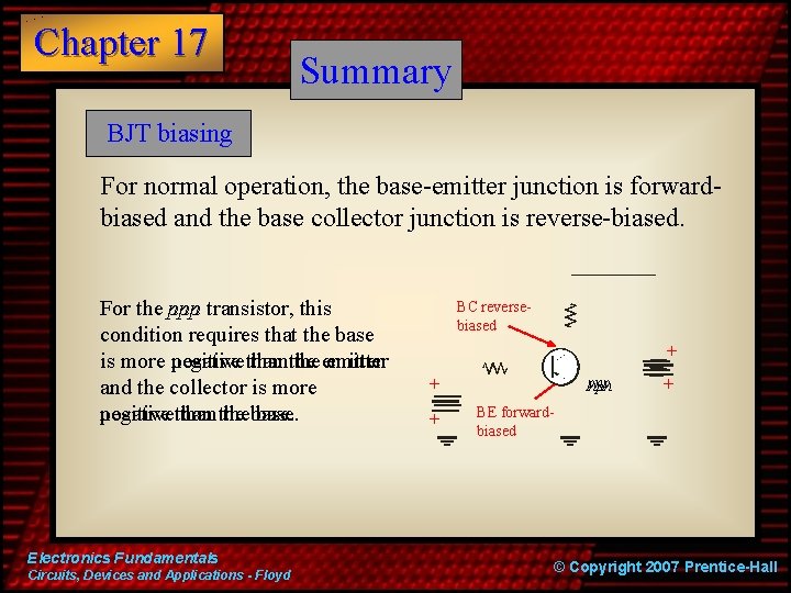
Chapter 17 Summary BJT biasing For normal operation, the base-emitter junction is forwardbiased and the base collector junction is reverse-biased. For the pnp npn transistor, this condition requires that the base is more negative positive than the emitter and the collector is more positive than negative thanthe base. Electronics Fundamentals Circuits, Devices and Applications - Floyd BC reversebiased + pnp npn + + + BE forwardbiased © Copyright 2007 Prentice-Hall

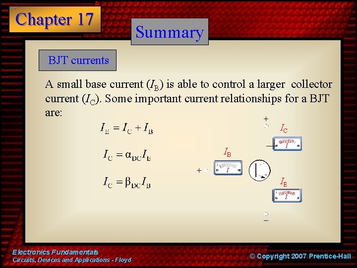
Chapter 17 Summary BJT currents A small base current (IB) is able to control a larger collector current (IC). Some important current relationships for a BJT are: IC IB I I IE I Electronics Fundamentals Circuits, Devices and Applications - Floyd © Copyright 2007 Prentice-Hall

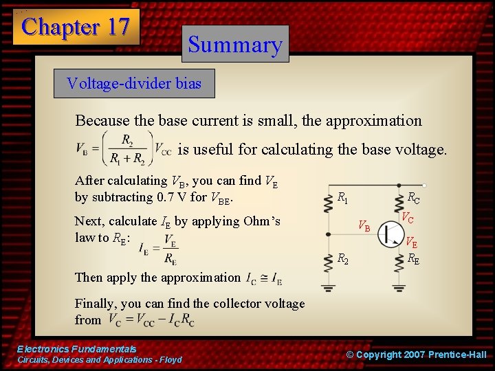
Chapter 17 Summary Voltage-divider bias Because the base current is small, the approximation is useful for calculating the base voltage. After calculating VB, you can find VE by subtracting 0. 7 V for VBE. R 1 Next, calculate IE by applying Ohm’s law to RE: RC VB R 2 VC VE RE Then apply the approximation Finally, you can find the collector voltage from Electronics Fundamentals Circuits, Devices and Applications - Floyd © Copyright 2007 Prentice-Hall

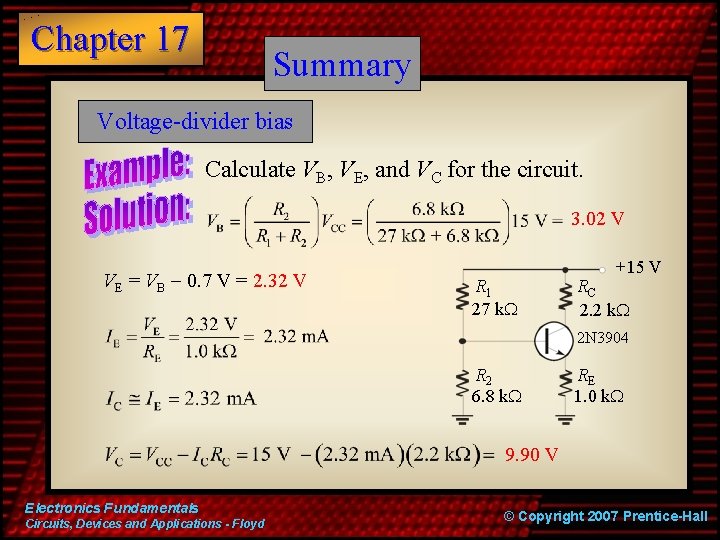
Chapter 17 Summary Voltage-divider bias Calculate VB, VE, and VC for the circuit. 3. 02 V VE = VB - 0. 7 V = 2. 32 V R 1 27 k. W +15 V RC 2. 2 k. W 2 N 3904 R 2 6. 8 k. W RE 1. 0 k. W 9. 90 V Electronics Fundamentals Circuits, Devices and Applications - Floyd © Copyright 2007 Prentice-Hall

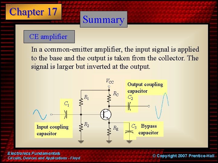
Chapter 17 Summary CE amplifier In a common-emitter amplifier, the input signal is applied to the base and the output is taken from the collector. The signal is larger but inverted at the output. VCC C 1 Input coupling capacitor Electronics Fundamentals Circuits, Devices and Applications - Floyd R 1 R 2 RC Output coupling capacitor C 2 RE C 3 Bypass capacitor © Copyright 2007 Prentice-Hall

Chapter 17 Summary CC amplifier In a common-collector amplifier, the input signal is applied to the base and the output is taken from the emitter. There is no voltage gain, but there is power gain. The output voltage is nearly the same as the input; there is no phase reversal as in the CE amplifier. The input resistance is larger than in the equivalent CE amplifier because the emitter resistor is not bypassed. Electronics Fundamentals Circuits, Devices and Applications - Floyd VCC C 1 R 2 RE © Copyright 2007 Prentice-Hall

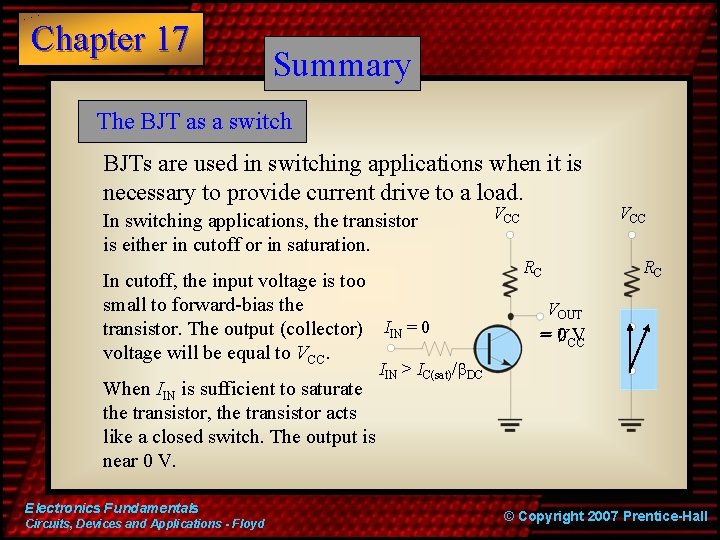
Chapter 17 Summary The BJT as a switch BJTs are used in switching applications when it is necessary to provide current drive to a load. In switching applications, the transistor is either in cutoff or in saturation. In cutoff, the input voltage is too small to forward-bias the transistor. The output (collector) IIN = 0 voltage will be equal to VCC. When IIN is sufficient to saturate the transistor, the transistor acts like a closed switch. The output is near 0 V. Electronics Fundamentals Circuits, Devices and Applications - Floyd VCC RC VOUT 0 CC V =V IIN > IC(sat)/b. DC © Copyright 2007 Prentice-Hall

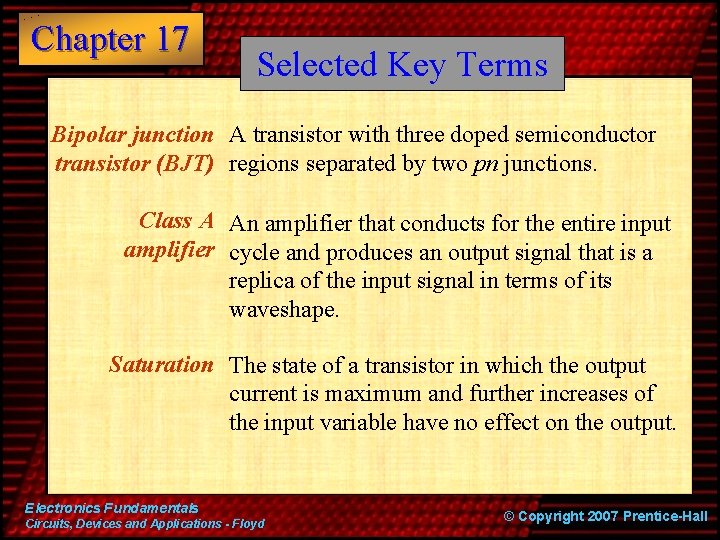
Chapter 17 Selected Key Terms Bipolar junction A transistor with three doped semiconductor transistor (BJT) regions separated by two pn junctions. Class A An amplifier that conducts for the entire input amplifier cycle and produces an output signal that is a replica of the input signal in terms of its waveshape. Saturation The state of a transistor in which the output current is maximum and further increases of the input variable have no effect on the output. Electronics Fundamentals Circuits, Devices and Applications - Floyd © Copyright 2007 Prentice-Hall

Chapter 17 Selected Key Terms Cutoff The non-conducting state of a transistor. Q-point The dc operating (bias) point of an amplifier. Amplification The process of producing a larger voltage, current or power using a smaller input signal as a pattern. Common- A BJT amplifier configuration in which the emitter (CE) emitter is the common terminal. Class B An amplifier that conducts for half the input amplifier cycle. Electronics Fundamentals Circuits, Devices and Applications - Floyd © Copyright 2007 Prentice-Hall

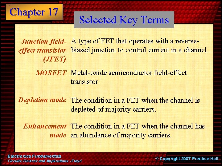
Chapter 17 Selected Key Terms Junction field- A type of FET that operates with a reverseeffect transistor biased junction to control current in a channel. (JFET) MOSFET Metal-oxide semiconductor field-effect transistor. Depletion mode The condition in a FET when the channel is depleted of majority carriers. Enhancement The condition in a FET when the channel has mode an abundance of majority carriers. Electronics Fundamentals Circuits, Devices and Applications - Floyd © Copyright 2007 Prentice-Hall

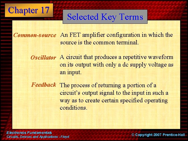
Chapter 17 Selected Key Terms Common-source An FET amplifier configuration in which the source is the common terminal. Oscillator A circuit that produces a repetitive waveform on its output with only a dc supply voltage as an input. Feedback The process of returning a portion of a circuit’s output signal to the input in such a way as to create certain specified operating conditions. Electronics Fundamentals Circuits, Devices and Applications - Floyd © Copyright 2007 Prentice-Hall