
Chapter 15 DIB Design n Purpose of the
Chapter 15 - DIB Design
n Purpose of the Device Interface Board – Definitions: n n DIB: Device Interface Board HIB: Handler Interface Board PIB: Prober Interface Board Electrical and mechanical interface between and ATE – Electrical Interface: n n n – Distributing the power and signals from the ATE to the DUT Signal conditioning to comply with DUT requirements Optimizing Tester efficiency by on DIB components Mechanical Interface: n n n Aligning the DUT from Handler/Prober to DUT contactor on DIB Comply with mechanical forces introduced by Handler/Prober when inserting DUT to socket Aligning the DIB to the test head of the ATE

Octal site RF Device Interface Board (DIB) Hand test socket with DUT Components for signal distribution and
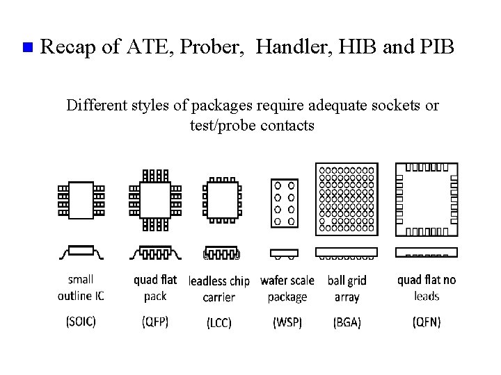
n Recap of ATE, Prober, Handler, HIB and PIB Different styles of packages require adequate sockets or test/probe contacts

Electromechanical relays modify the DUT’s electrical environment ATE DUT output Relay (open) 1 k load Leakage test setup DUT output 1 k load Relay (closed by test program) Distortion test setup
n DIB Basics – Purpose of the Device Interface Board – – – DUTs that are purely digital in nature typically require a very simple DIB that simply provides point-to-point connectivity between the DUT pins and the tester’s power supplies and digital pin card electronics. Analog and mixed-signal DUTs usually require much more elaborate DIBs. • In fact, DIB design is a fairly major part of mixed-signal test development. A mixed-signal DIB will often contain a variety of active and passive circuits that must be connected to (or disconnected from) various DUT pins as the test program progresses.
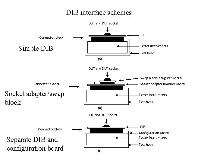
DIB interface schemes DUT and DUT socket DIB Connector block Tester instruments Simple DIB Test head (a) DUT and DUT socket Swap block (daughter board) Connector blocks Socket adapter/swap block Socket adapter (mother board) Tester instruments Test head (b) DUT and DUT socket DIB Connector block Separate DIB and configuration board Configuration board Tester instruments Test head (c)
n DIB Basics – Importance of good DIB Design – – – One of the major causes of long test program development time is poor mixed-signal DIB design and printed circuit board design and layout. A DIB schematic shows only an idealized view of the DIB. Resistors are shown as ideal resistances, capacitors as ideal capacitances, and traces as perfect connections with no parasitic inductance or capacitance. In reality, the exact mechanical layout of the components and traces on the DIB may make the difference between failing test results and passing results.
n DIB Basics – Importance of good DIB Design – – – The performance of analog and mixed-signal devices is highly dependent on the quality of the surrounding circuit design. • It is important to be able to distinguish between legitimate DUT failures and failures caused by poor design of the DIB. Unfortunately, it is difficult to provide the DUT with a perfect environment using a general-purpose tester with bulky electromechanical interconnections. • For example, the pins of the DUT socket will typically add more inductance and capacitance with an increased cross coupling to the DUT’s environment than it will see when it is soldered directly onto a printed circuit board in the final application. Nevertheless, the test engineer has to try to design a DIB that does not present the DUT with electrical handicaps.
n Printed Circuit Boards (PCBs) – PCB CAD Tools – Using a netlist-compatible schematic capture tool, the test engineer draws the circuit schematic on a computer workstation or PC using the seed job for the DIB he decided to use. – Then the schematic database is transferred to the PCB designer for use in the DIB layout process. The layout (footprints) of the components are in the layout level of the design tool – Once the netlist has been extracted from the database, the PCB designer begins laying out the DIB from a standard DIB template. – The DIB seedjob represents a head-start DIB design, which includes the shape of the DIB and its standard mechanical mounting holes as well as many pre-placed standard components, such as tester connectors and pogo pads and keep out areas.
n Printed Circuit Boards (PCBs) – PCB CAD Tools – – The netlist directs the PCB layout software to import all the required DIB components from a standard parts library. The PCB designer then places these components and connects them as shown in the schematic. The netlist prevents errors in point-to-point connections by refusing to let the layout designer place traces where they do not belong. The netlist also guarantees that none of the desired connections are mistakenly omitted. Once the DIB layout is completed, each layer of the design is plotted onto transparent film for use in PCB fabrication. These plots are commonly known as Gerbers, or Gerber plots, named after the company that pioneered some of the early plotting equipment (Gerber Scientific)
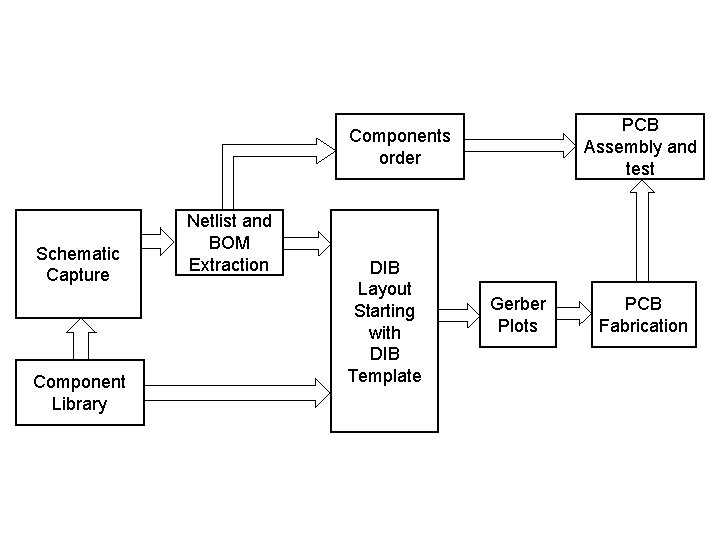
PCB Assembly and test Components order Schematic Capture Component Library Netlist and BOM Extraction DIB Layout Starting with DIB Template Gerber Plots PCB Fabrication
n Printed Circuit Boards (PCBs) – Multilayer PCBs n Low-cost PCBs can be designed and fabricated using one or two layers of copper trace. n Traces on opposite sides of a double-layer PCB can be connected using a copper plated through-hole called a via. n Double-layer PCB fabrication starts with a blank PCB consisting of a sheet of insulator (e. g. fiberglass) plated on both sides with a thin layer of copper. n The component lead holes and vias are drilled first. n Then the holes are plated with copper to form the layer-tolayer interconnects. n Finally, the traces are printed and etched using a photolithographic process similar to that used in IC fabrication
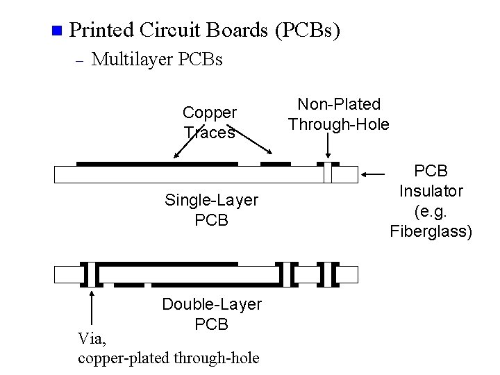
n Printed Circuit Boards (PCBs) – Multilayer PCBs Copper Traces Single-Layer PCB Double-Layer PCB Via, copper-plated through-hole Non-Plated Through-Hole PCB Insulator (e. g. Fiberglass)
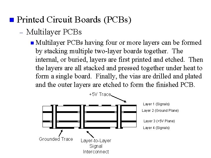
n Printed Circuit Boards (PCBs) – Multilayer PCBs n Multilayer PCBs having four or more layers can be formed by stacking multiple two-layer boards together. The internal, or buried, layers are first printed and etched. Then the layers are all stacked and pressed together under heat to form a single board. Finally, the vias are drilled and plated and the outer layers are etched to form the finished PCB. +5 V Trace Layer 1 (Signals) Layer 2 (Ground Plane) Layer 3 (+5 V Plane) Layer 4 (Signals) Grounded Trace Layer-to-Layer Signal Interconnect
n Printed Circuit Boards (PCBs) – Multilayer PCBs n Most mixed-signal DIBs are formed using 6 - to 30 -layer PCBs. The arrangement of layers in a PCB is known as the stackup. n The stackup of a DIB may vary from one type of DUT to another, but there are some general guidelines that are commonly followed. n The internal layers are typically used for ground and power distribution n Internal layer can be used to shield critical traces between two ground planes (layer). n The outer layers are usually reserved for critical signals or those signal traces that might need to be modified after the DIB has been fabricated.
n Printed Circuit Boards (PCBs) – Multilayer PCBs n In addition to the trace layers and insulator layers in a PCB, the outer layers are usually coated with a material called a solder mask. This thin non-conductive layer keeps solder from flowing all over the traces when the DIB components are soldered onto the PCB. The soldermask helps to prevent unwanted solder shorts between adjacent traces. n A silkscreened pattern may also be printed on the outer layers of the PCB. The silkscreened patterns show the outline and reference numbers for all the DIB components, such as resistors, capacitors, relays, and connectors and the DUTs. The silkscreened patterns are quite useful during the DIB component assembly process and they are equally useful during the test program debugging process.
n Printed Circuit Boards (PCBs) – PCB Materials n Printed circuit boards can be constructed using a variety of materials. n The most common trace material is copper, due to its excellent electrical conductivity. n The most common insulator material is FR 4 (fire retardant, type 4) fiberglass. Fiberglass is an inexpensive material that exhibits good electrical properties up to several hundred megahertz. As frequencies approach 1 GHz, more exotic materials such as Teflon or cynate ester may be used.
n Printed Circuit Boards (PCBs) – PCB Materials n Teflon * exhibits excellent microwave characteristics, including low signal loss and a low dielectric constant. However, it suffers from poor mechanical stiffness. n Cynate ester is a material with reasonably good high frequency properties and yet it is stiff enough to withstand the mechanical stress of production testing. n One possible compromise between the good electrical properties of Teflon and the good mechanical properties of cynate ester is a hybrid stackup consisting of sandwiched layers of Teflon and either FR 4 or cynate ester
n DIB Traces, Shields and Ground – Trace Parasitics n One of the most important DIB components is the printed circuit board (PCB) trace. n It is easy to think that wires and traces are not components at all, but are instead represented by the connecting lines that appear in a schematic. However, PCB traces are slightly resistive, slightly inductive, and slightly capacitive in nature. n Often, trace parasitics can be ignored, especially when working with low frequencies and low to moderate current levels. Other times, the parasitics will have a significant effect on a circuit’s behavior. The test engineer should always be aware of the potential problems that trace parasitics might pose.
n DIB Traces, Shields and Ground – Trace Parasitics n Trace resistance on DIBs seldom exceeds a few Ohms. n Inductance can be anywhere from one or two nanohenrys to several microhenrys. n Capacitance can range from one or two picofarads to tens of picofarads. n Although these values are very approximate, they can be used as a thumbnail estimate to determine whether the parasitic elements might be large enough to affect the DUT’s performance. n To estimate trace parasitics with a little more accuracy, we need to review the equations for trace resistance, inductance, and capacitance.
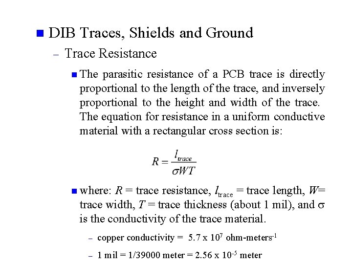
n DIB Traces, Shields and Ground – Trace Resistance n The parasitic resistance of a PCB trace is directly proportional to the length of the trace, and inversely proportional to the height and width of the trace. The equation for resistance in a uniform conductive material with a rectangular cross section is: n where: R = trace resistance, ltrace = trace length, W= trace width, T = trace thickness (about 1 mil), and s is the conductivity of the trace material. – copper conductivity = 5. 7 x 10⁷ ohm-meters-1 – 1 mil = 1/39000 meter = 2. 56 x 10 -5 meter

n Problem – Calculate the parasitic resistance of a PCB trace that is 15 inches long, 1 mil thick, and 20 mils wide. n Solution: – – – First we convert all units of length into meters: L = 15 inches * (1 meter / 39 inches) = 0. 38462 meters T = 1 mil * (1 meter / 39370 mils) = 2. 54 x 10 -5 meters W = 20 mil * (1 meter / 39370 mils) = 5. 08 x 10 -4 meters Applying the previous equation to a copper trace, we get a total parasitic resistance of:
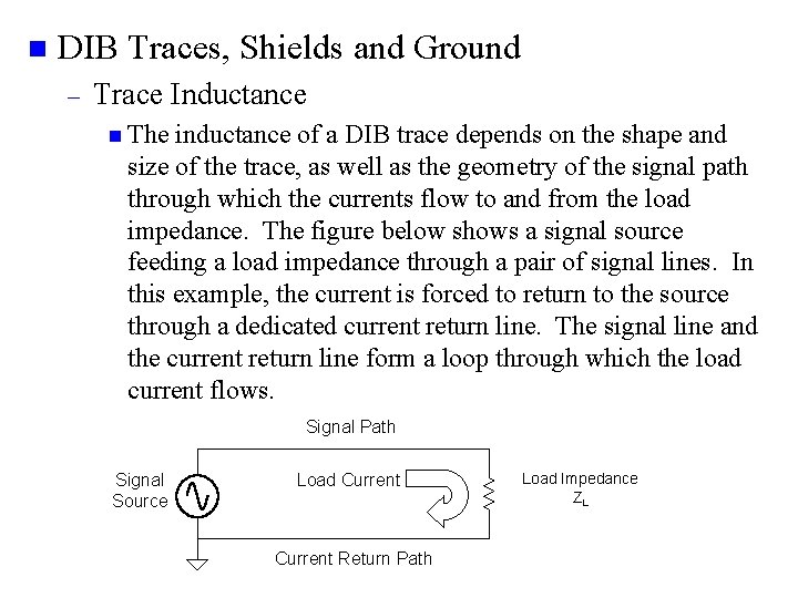
n DIB Traces, Shields and Ground – Trace Inductance n The inductance of a DIB trace depends on the shape and size of the trace, as well as the geometry of the signal path through which the currents flow to and from the load impedance. The figure below shows a signal source feeding a load impedance through a pair of signal lines. In this example, the current is forced to return to the source through a dedicated current return line. The signal line and the current return line form a loop through which the load current flows. Signal Path Signal Source Load Current Return Path Load Impedance ZL
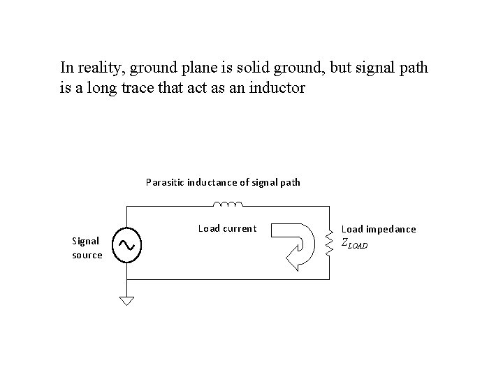
In reality, ground plane is solid ground, but signal path is a long trace that act as an inductor Parasitic inductance of signal path Signal source Load current Load impedance ZLOAD
n DIB Traces, Shields and Ground – Trace Inductance n We wish to minimize the effects of parasitic trace inductance on the DUT and DIB circuits. There a number of ways to reduce this inductance. – – Minimize the area enclosed by the load current path. One easy way to do this is to lay a dedicated current return trace along side the signal trace. Another way to obtain low inductance is to use a solid ground plane as the return path for all signals. By routing each signal trace over a solid ground plane close in the stack up, thus the load current can return underneath the trace along a path with very low cross sectional area. Another way to reduce inductance is to make the trace as wide as is practical, since a wide trace over a ground plane has minimal inductance.
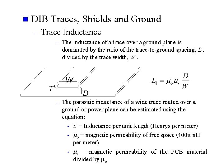
n DIB Traces, Shields and Ground – Trace Inductance – The inductance of a trace over a ground plane is dominated by the ratio of the trace-to-ground spacing, D, divided by the trace width, W. W T D – The parasitic inductance of a wide trace routed over a ground or power plane can be estimated using the equation: • Ll = Inductance per unit length (Henrys per meter) • mo = magnetic permeability of free space (400 p n. H per meter) • mr = magnetic permeability of the PCB material divided by mo
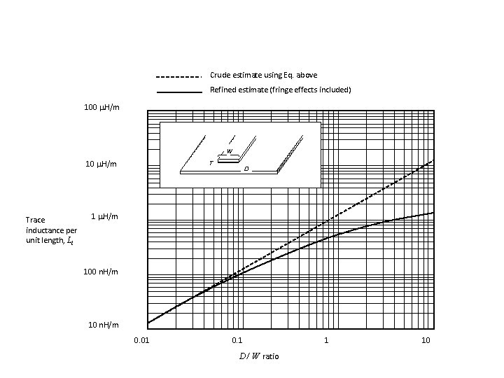
Crude estimate using Eq. above Refined estimate (fringe effects included) 100 m. H/m W 10 m. H/m Trace inductance per unit length, Ll T D 1 m. H/m 100 n. H/m 10 n. H/m 0. 01 0. 1 D / W ratio 1 10
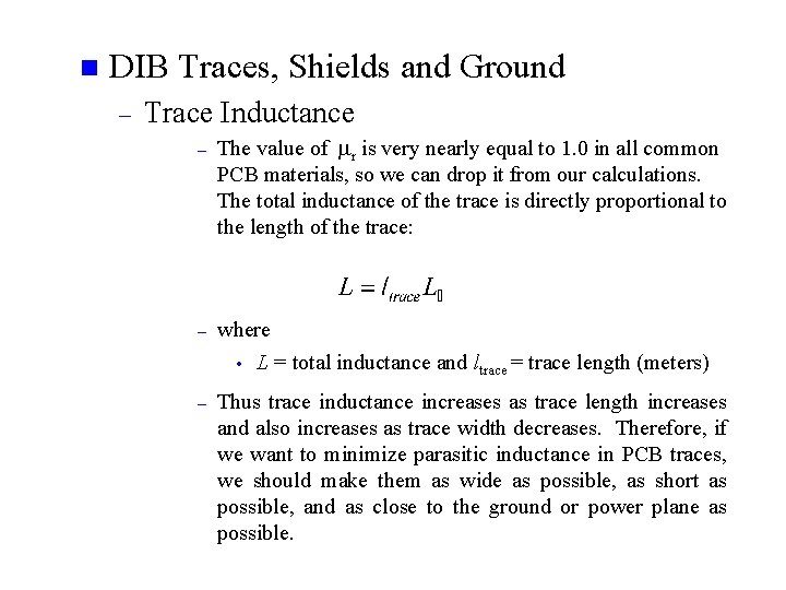
n DIB Traces, Shields and Ground – Trace Inductance – The value of mr is very nearly equal to 1. 0 in all common PCB materials, so we can drop it from our calculations. The total inductance of the trace is directly proportional to the length of the trace: – where • L = total inductance and ltrace = trace length (meters) – Thus trace inductance increases as trace length increases and also increases as trace width decreases. Therefore, if we want to minimize parasitic inductance in PCB traces, we should make them as wide as possible, as short as possible, and as close to the ground or power plane as possible.
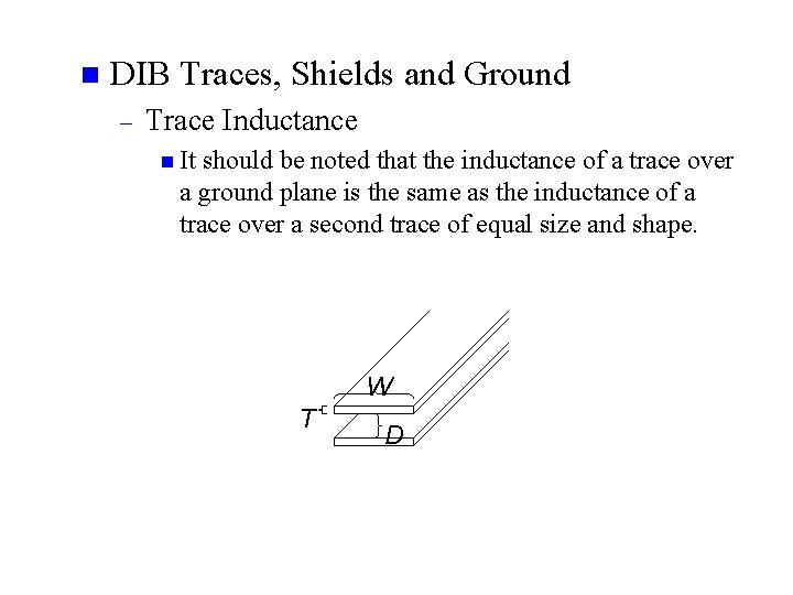
n DIB Traces, Shields and Ground – Trace Inductance n It should be noted that the inductance of a trace over a ground plane is the same as the inductance of a trace over a second trace of equal size and shape. W T D

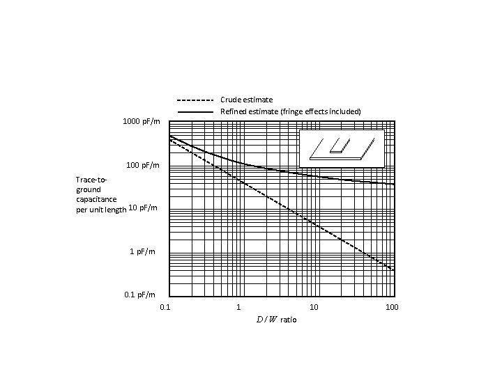
n DIB Traces, Shields and Ground – Trace Capacitance n The capacitance between two parallel traces can be estimated using the standard parallel plate capacitance equation. The parasitic capacitance between two metal plates of area A is given by the equation: n Where: A = area of either plate D = distance between the plates eo = electrical permittivity of free space (8. 8542 x 10 -12 F/m) er = relative permittivity of the dielectric material
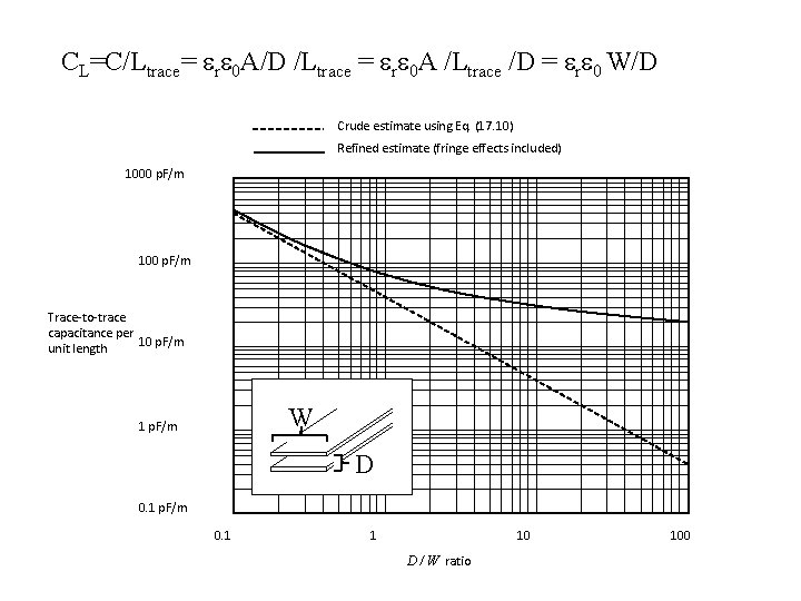
CL=C/Ltrace= ere 0 A/D /Ltrace = ere 0 A /Ltrace /D = ere 0 W/D Crude estimate using Eq. (17. 10) Refined estimate (fringe effects included) 1000 p. F/m 100 p. F/m Trace-to-trace capacitance per 10 p. F/m unit length W 1 p. F/m D 0. 1 p. F/m 0. 1 1 10 D / W ratio 100
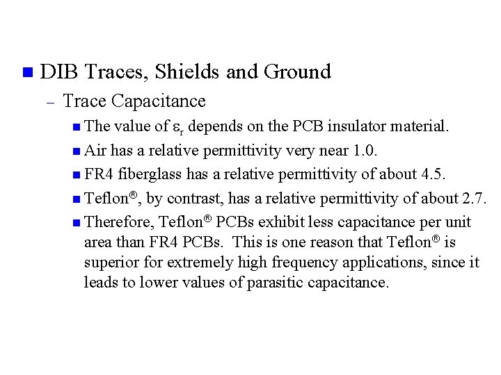
n DIB Traces, Shields and Ground – Trace Capacitance n The value of er depends on the PCB insulator material. n Air has a relative permittivity very near 1. 0. n FR 4 fiberglass has a relative permittivity of about 4. 5. n Teflon , by contrast, has a relative permittivity of about 2. 7. n Therefore, Teflon PCBs exhibit less capacitance per unit area than FR 4 PCBs. This is one reason that Teflon is superior for extremely high frequency applications, since it leads to lower values of parasitic capacitance.
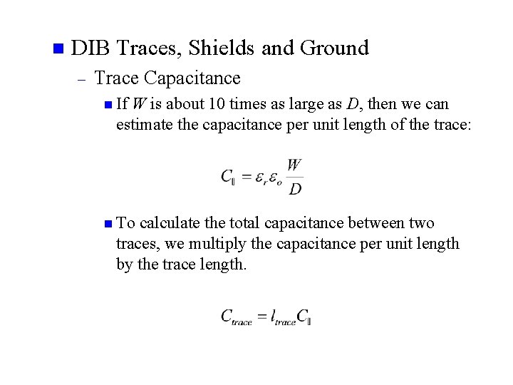
n DIB Traces, Shields and Ground – Trace Capacitance n If W is about 10 times as large as D, then we can estimate the capacitance per unit length of the trace: n To calculate the total capacitance between two traces, we multiply the capacitance per unit length by the trace length.
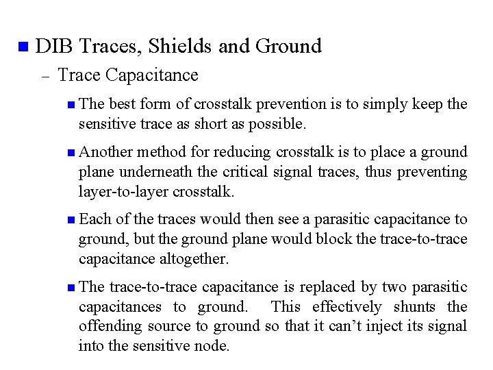
n DIB Traces, Shields and Ground – Trace Capacitance n The best form of crosstalk prevention is to simply keep the sensitive trace as short as possible. n Another method for reducing crosstalk is to place a ground plane underneath the critical signal traces, thus preventing layer-to-layer crosstalk. n Each of the traces would then see a parasitic capacitance to ground, but the ground plane would block the trace-to-trace capacitance altogether. n The trace-to-trace capacitance is replaced by two parasitic capacitances to ground. This effectively shunts the offending source to ground so that it can’t inject its signal into the sensitive node.
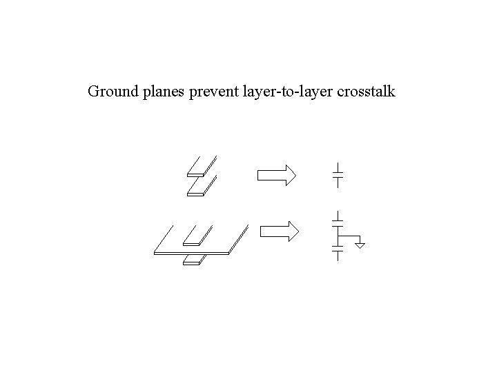
Ground planes prevent layer-to-layer crosstalk
Crude estimate Refined estimate (fringe effects included) 1000 p. F/m 100 p. F/m Trace-toground capacitance per unit length 10 p. F/m 1 p. F/m 0. 1 1 10 D / W ratio 100
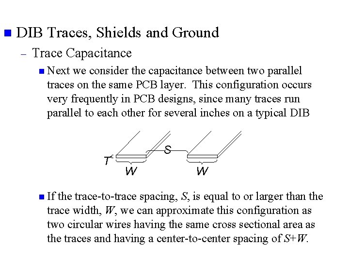
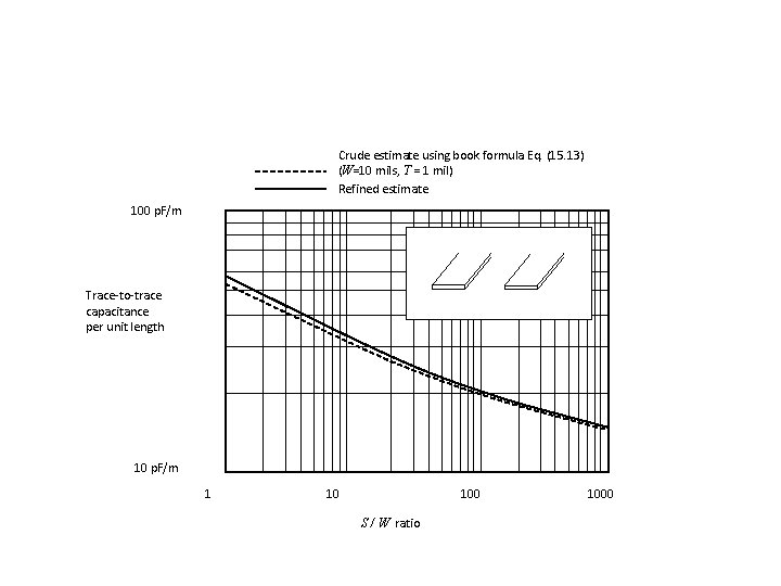
n DIB Traces, Shields and Ground – Trace Capacitance n Next we consider the capacitance between two parallel traces on the same PCB layer. This configuration occurs very frequently in PCB designs, since many traces run parallel to each other for several inches on a typical DIB T S W W n If the trace-to-trace spacing, S, is equal to or larger than the trace width, W, we can approximate this configuration as two circular wires having the same cross sectional area as the traces and having a center-to-center spacing of S+W.
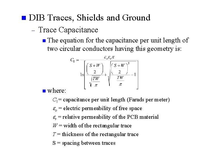
n DIB Traces, Shields and Ground – Trace Capacitance n The equation for the capacitance per unit length of two circular conductors having this geometry is: n where: Cl = capacitance per unit length (Farads per meter) eo = electric permeability of free space er = relative permeability of the PCB material W = width of the rectangular trace T = thickness of the rectangular trace S = spacing between traces
Crude estimate using book formula Eq. (15. 13) (W=10 mils, T = 1 mil) Refined estimate 100 p. F/m Trace-to-trace capacitance per unit length 10 p. F/m 1 10 100 S / W ratio 1000
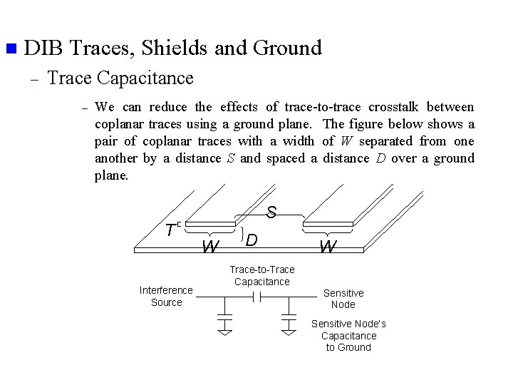
n DIB Traces, Shields and Ground – Trace Capacitance – We can reduce the effects of trace-to-trace crosstalk between coplanar traces using a ground plane. The figure below shows a pair of coplanar traces with a width of W separated from one another by a distance S and spaced a distance D over a ground plane. T Interference Source S W D Trace-to-Trace Capacitance W Sensitive Node’s Capacitance to Ground
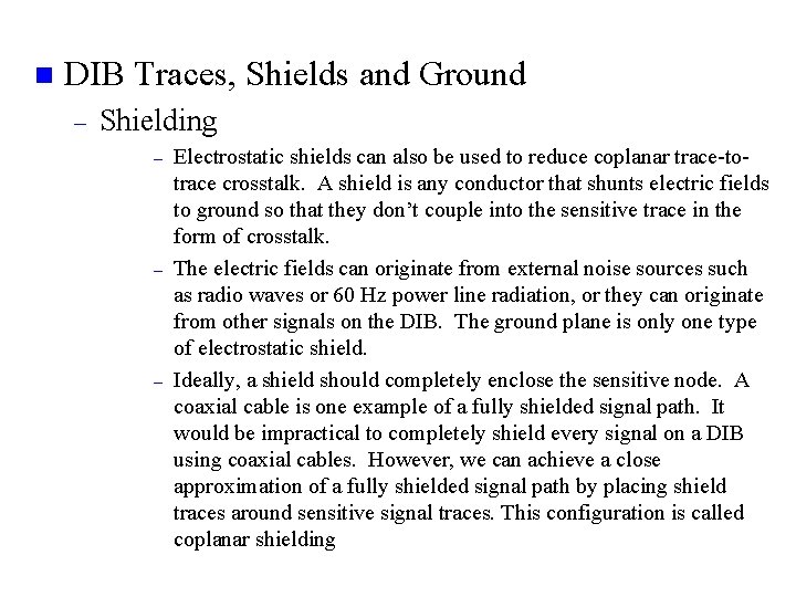
n DIB Traces, Shields and Ground – Shielding – – – Electrostatic shields can also be used to reduce coplanar trace-totrace crosstalk. A shield is any conductor that shunts electric fields to ground so that they don’t couple into the sensitive trace in the form of crosstalk. The electric fields can originate from external noise sources such as radio waves or 60 Hz power line radiation, or they can originate from other signals on the DIB. The ground plane is only one type of electrostatic shield. Ideally, a shield should completely enclose the sensitive node. A coaxial cable is one example of a fully shielded signal path. It would be impractical to completely shield every signal on a DIB using coaxial cables. However, we can achieve a close approximation of a fully shielded signal path by placing shield traces around sensitive signal traces. This configuration is called coplanar shielding

n DIB Traces, Shields and Ground – Shielding n Coplanar shielding can reduce crosstalk between a interference source and a sensitive DIB signal. The shield trace is connected to the ground plane to provide an extra level of protection for the sensitive node. Another benefit of shield traces is that they help to reduce the coupling of electromagnetic interference such as radio and TV signals Interference Source Shield Trace Sensitive Node

n DIB Traces, Shields and Ground – Shielding n Sometimes, a shield trace will be routed all the way around a sensitive node. Interference Signal Sensitive Node Grounded Shield Ring
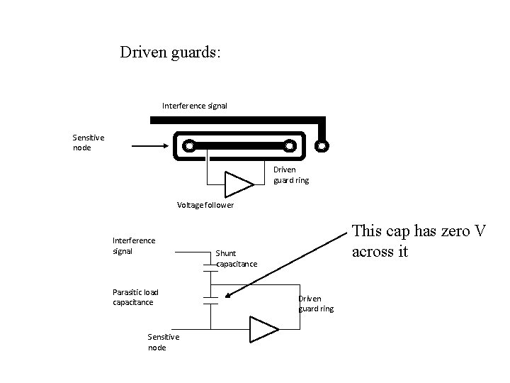
Driven guards: Interference signal Sensitive node Driven guard ring Voltage follower Interference signal Parasitic load capacitance Sensitive node This cap has zero V across it Shunt capacitance Driven guard ring
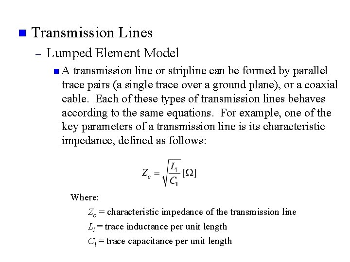
n Transmission Lines – Lumped Element Model n A transmission line or stripline can be formed by parallel trace pairs (a single trace over a ground plane), or a coaxial cable. Each of these types of transmission lines behaves according to the same equations. For example, one of the key parameters of a transmission line is its characteristic impedance, defined as follows: Where: Zo = characteristic impedance of the transmission line Ll = trace inductance per unit length Cl = trace capacitance per unit length
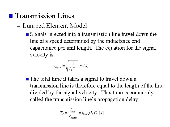
n Transmission Lines – Lumped Element Model n Signals injected into a transmission line travel down the line at a speed determined by the inductance and capacitance per unit length. The equation for the signal velocity is: n The total time it takes a signal to travel down a transmission line is therefore equal to the length of the line divided by the signal velocity. This time is commonly called the transmission line’s propagation delay:
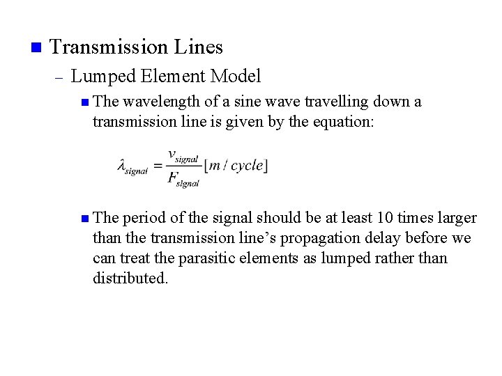
n Transmission Lines – Lumped Element Model n The wavelength of a sine wave travelling down a transmission line is given by the equation: n The period of the signal should be at least 10 times larger than the transmission line’s propagation delay before we can treat the parasitic elements as lumped rather than distributed.
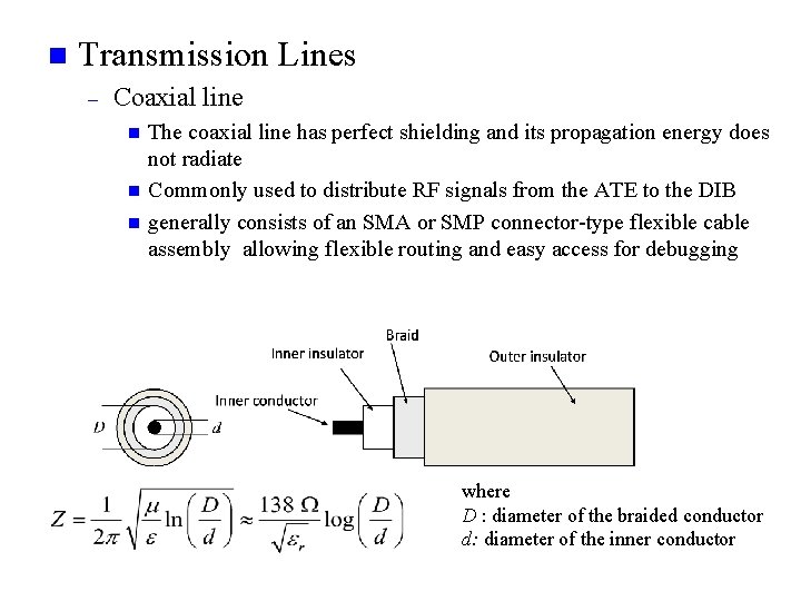
n Transmission Lines – Coaxial line n n n The coaxial line has perfect shielding and its propagation energy does not radiate Commonly used to distribute RF signals from the ATE to the DIB generally consists of an SMA or SMP connector-type flexible cable assembly allowing flexible routing and easy access for debugging where D : diameter of the braided conductor d: diameter of the inner conductor
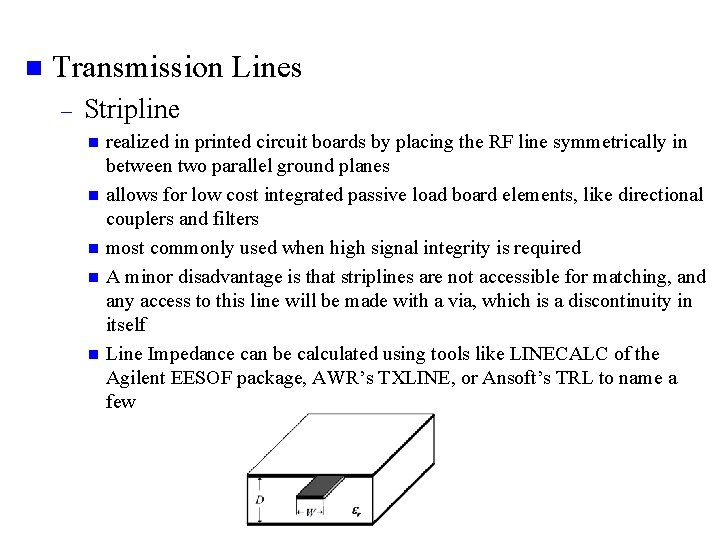
n Transmission Lines – Stripline realized in printed circuit boards by placing the RF line symmetrically in between two parallel ground planes n allows for low cost integrated passive load board elements, like directional couplers and filters n most commonly used when high signal integrity is required n A minor disadvantage is that striplines are not accessible for matching, and any access to this line will be made with a via, which is a discontinuity in itself n Line Impedance can be calculated using tools like LINECALC of the Agilent EESOF package, AWR’s TXLINE, or Ansoft’s TRL to name a few n
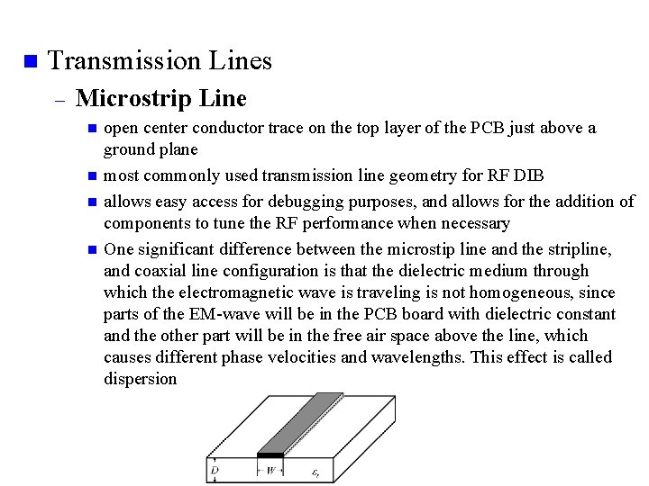
n Transmission Lines – Microstrip Line n n open center conductor trace on the top layer of the PCB just above a ground plane most commonly used transmission line geometry for RF DIB allows easy access for debugging purposes, and allows for the addition of components to tune the RF performance when necessary One significant difference between the microstip line and the stripline, and coaxial line configuration is that the dielectric medium through which the electromagnetic wave is traveling is not homogeneous, since parts of the EM-wave will be in the PCB board with dielectric constant and the other part will be in the free air space above the line, which causes different phase velocities and wavelengths. This effect is called dispersion
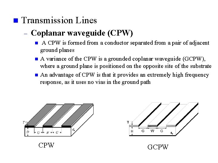
n Transmission Lines – Coplanar waveguide (CPW) n n n A CPW is formed from a conductor separated from a pair of adjacent ground planes A variance of the CPW is a grounded coplanar waveguide (GCPW), where a ground plane is positioned on the opposite of the substrate An advantage of CPW is that it provides an extremely high frequency response, as it uses no vias in the ground path CPW GCPW
n Transmission Lines Discontinuities – – Every time when an EM wave hits a discontinuity in a transmission line, the RF current will crowd which will behave like an inductor, or the electrical field will fringe which has a capacitance nature. For a best and most simple design of a RF DIB it is recommended, to avoid any line discontinuities it is obvious, that RF lines can’t be connected in a Tee or Cross configuration without simulating this new RF element with a RF simulation Performance impact of line discontinuities are shown in the next slide
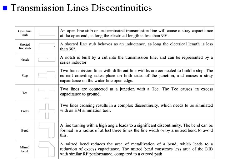
n Transmission Lines Discontinuities
n Transmission Lines – Transmission Line Termination n To understand the purpose of transmission line termination, let us first examine the behavior of an unterminated line. An unterminated transmission line behaves as a sort of electronic echo chamber. If we transmit a stepped voltage down an unterminated transmission line, it will bounce back and forth between the ends of the line until parasitic resistance in the line eventually causes the echoes to die out. The resulting reflections appear as undesirable ringing on the stepped signal. Properly chosen termination resistors placed at either the source side or the load side of a transmission line cause it to behave in a much simpler manner than it would behave without termination. The purpose of termination resistors is to dissipate the energy in the transmitted signal so that reflections do not occur.
n Transmission Lines – Transmission Line Termination n If the termination resistor RT is equal to the characteristic impedance of the transmission line, then the transmitted signal will not reflect at all. The energy associated with the currents and voltages propagating along the transmission line is completely dissipated by the termination resistor. As far as the signal source is concerned, a terminated transmission line looks just like a resistor whose value is equal to Zo. The distributed inductance and capacitance of the transmission line completely disappear as far as the source is concerned. – The only difference between a purely resistive load and a terminated transmission line is that the signal reaching the termination resistor is delayed by the propagation delay of the transmission line. Also it is important to note that while the termination resistor is usually connected to ground, it can be set to any DC voltage and the transmission line will still be properly terminated.
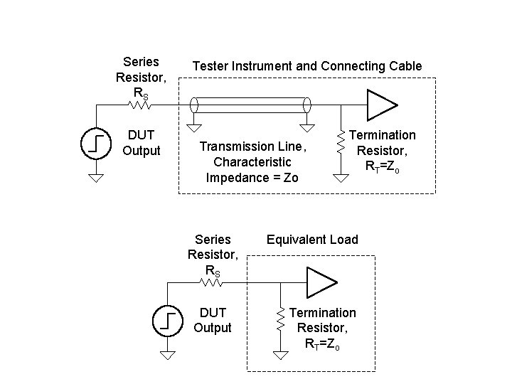
Series Resistor, RS DUT Output Tester Instrument and Connecting Cable Transmission Line, Characteristic Impedance = Zo Series Resistor, RS DUT Output Termination Resistor, RT=Zo Equivalent Load Termination Resistor, RT=Zo
n Transmission Lines – Transmission Line Termination n The ability to treat a terminated transmission line as a purely resistive element is very useful. Many tester instruments are connected to the DUT through a 50 transmission line which is terminated with a 50 resistor at the instrument’s input (on the previous slide). As far as the DUT is concerned, this instrument looks just like a 50 resistor attached between its output and ground. If the DUT output is unable to drive such a low impedance, then we can add a resistor, RS, between the DUT output and the terminated transmission line. The DUT output then sees a purely resistive load equal to RS+Z 0. The signal amplitude is reduced by a factor of Z 0/(Z 0+RS), but we can compensate for this gain error using a calibration factor.
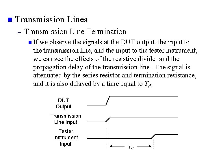
n Transmission Lines – Transmission Line Termination n If we observe the signals at the DUT output, the input to the transmission line, and the input to the tester instrument, we can see the effects of the resistive divider and the propagation delay of the transmission line. The signal is attenuated by the series resistor and termination resistance, and it is also delayed by a time equal to Td. DUT Output Transmission Line Input Tester Instrument Input Td
n Transmission Lines – Transmission Line Termination n One of the common mistakes made by novice test engineers is to observe the output of a digital channel at the point where the DIB connects to the test head. Such an observation point represents an intermediate point along the cascaded transmission line. As a result, a rising edge will appear as a pair of transitions rather than a single transition. The novice test engineer often thinks the tester driver is defective, when in fact it is working just fine. The only way to see the correct signal is to observe it at the DUT’s input.
n Transmission Lines – Transmission Line Termination n Notice that we can measure the propagation delay of a transmission line by measuring the time between the first and second step transitions at the source end of a sourceterminated transmission line. This time is equal to 2*Td. We can divide the measured time by two to calculate the transmission line’s propagation delay. This is how modern testers measure the propagation delays from the digital channel card drivers to the DUT’s digital inputs. The tester can automatically compensate for the electrical delay in each transmission line, thereby removing timing skew from the digital signals. This deskewing process is known as time domain reflectometry, or TDR.
n Grounding and Power Distribution – Grounding n n n The term “grounding” refers to the electrical interconnection and physical layout of the various ground nodes in an electronic system such as an ATE tester and DIB. The Test Engineer needs to remember when placing a Ground node, that the ground path is as important as the signal path and represents the return path of the signal to the ATE or DUT In a circuit schematic, grounds are treated as perfect zero volt reference points exhibiting zero impedance. In a real system, there can be only one point that is defined as true ground. All other ground nodes are connected to true ground through resistive and inductive traces, wires, or ground planes. Often, these parasitic resistors and inductors play a significant role in the performance of the DUT and the ATE tester instruments.
n Grounding and Power Distribution – Grounding n One way to achieve proper grounding is to pay close attention to the flow of currents through the traces, wires, and planes in the DIB and tester. The first thing we have to consider is DC measurement errors caused by resistive drops in ground connections. The figure on the following slide shows a simple test setup including a DC current source, a DC voltmeter, and a DUT (a simple load resistor in this case). We wish to measure the value of the resistor by forcing a current, ITEST, and measuring the voltage drop across the resistor, VTEST. The resistor’s value is calculated by dividing VTEST by ITEST.
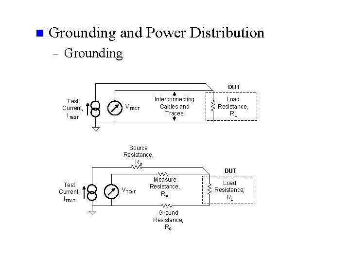
n Grounding and Power Distribution – Grounding DUT Test Current, ITEST Interconnecting Cables and Traces VTEST Load Resistance, RL Source Resistance, RS DUT Test Current, ITEST VTEST Measure Resistance, RM Ground Resistance, RG Load Resistance, RL
n Grounding and Power Distribution – Grounding n Obviously, accurate mixed-signal testers can not be constructed using such a simple grounding scheme. Instead, they use a signal which we will call device ground sense, or DGS, to carry the DUT’s 0 Volt reference back to each tester instrument. Since the DGS signal is carried on a network of zero-current wires, the series resistances of these wires do not result in voltage measurement errors. Any number of tester instruments can use the DGS line as a zero volt reference, provided that they do not pull current from DGS. Consequently, each tester instrument typically contains a high input impedance voltage follower to buffer the voltage on DGS.
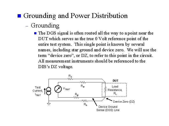
n Grounding and Power Distribution – Grounding n The DGS signal is often routed all the way to a point near the DUT which serves as the true 0 Volt reference point of the entire test system. This single point is known by several names, including star ground and device zero. We will use the term “device zero”, or DZ, to refer to this point in the circuit. All measurement instruments should be referenced to the DIB’s DZ voltage. RS DUT Test Current, ITEST RM VTEST RM RG Load Resistance, RL Device Zero (DZ) Device Ground Sense (DGS) Line
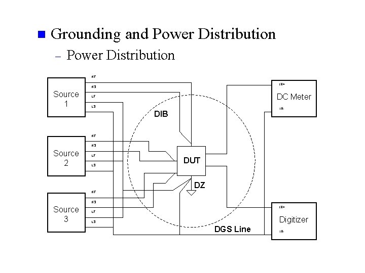
n Grounding and Power Distribution – Power Distribution HF IN+ HS Source 1 DC Meter LF LS IN- DIB HF HS Source 2 LF LS DUT DZ HF HS Source 3 IN+ LF Digitizer LS DGS Line IN-
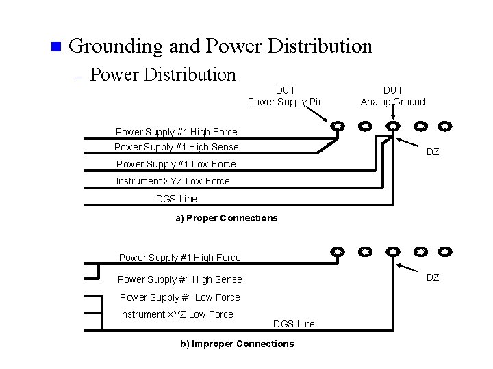
n Grounding and Power Distribution – Power Distribution DUT Power Supply Pin DUT Analog Ground Power Supply #1 High Force Power Supply #1 High Sense DZ Power Supply #1 Low Force Instrument XYZ Low Force DGS Line a) Proper Connections Power Supply #1 High Force DZ Power Supply #1 High Sense Power Supply #1 Low Force Instrument XYZ Low Force DGS Line b) Improper Connections
n Grounding and Power Distribution – Power and Ground Planes n The ground plane provides a low inductance connection between all the grounds on a DIB. Similarly, power supplies can be routed using power planes to reduce the series inductance between all power supply nodes. Power and ground planes can be divided into sections, forming what are known as split planes. Each section of a split plane can carry a different signal, such as +12 V, +5 V, and – 5 V. This provides the electrical superiority of copper planes without requiring a separate plane for each supply. Typically, power is applied through split planes while grounds are connected to solid (non-split) planes.
n Grounding and Power Distribution – Power and Ground Planes n There are usually at least two separate ground planes in any mixed-signal DIB. One plane forms the ground for the transmission line traces carrying digital signals. This plane is subject to rapidly changing current flows from the digital signals, and therefore exhibits fairly large voltage spikes caused by the interactions of the currents with its own inductance. This ground plane is often called DGND (digital ground) in the DIB schematics. n The second plane, AGND (analog ground), is for use by analog circuits. Ideally, this plane should carry only low frequency, low current signals that will not give rise to voltage spikes.
n Grounding and Power Distribution – Power and Ground Planes n A third plane is sometimes used as a DIB-wide zero volt reference. This “quiet ground” plane (QGND) can be used by analog circuits on the DIB that need a low noise ground reference. This plane must be connected in such a way that it does not carry any currents exceeding a few milliamps. It should be tied only to the DZ node at a single point and to relatively high impedance DUT pins and DIB circuit nodes. Often, the analog ground plane and the quiet ground plane are combined into a single plane, resulting in a DIB with only two ground planes (analog and digital).
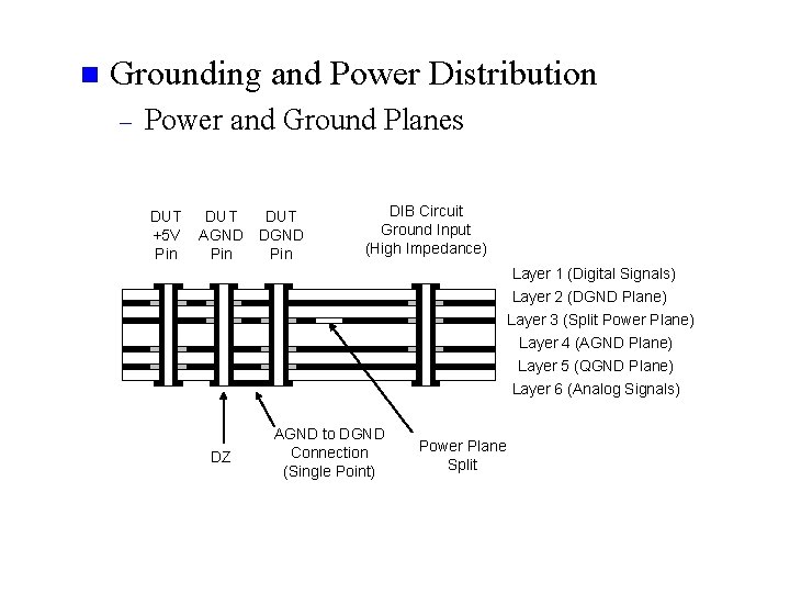
n Grounding and Power Distribution – Power and Ground Planes DUT +5 V Pin DUT AGND DGND Pin DIB Circuit Ground Input (High Impedance) Layer 1 (Digital Signals) Layer 2 (DGND Plane) Layer 3 (Split Power Plane) Layer 4 (AGND Plane) Layer 5 (QGND Plane) Layer 6 (Analog Signals) DZ AGND to DGND Connection (Single Point) Power Plane Split
n Grounding and Power Distribution – Ground Loops n A star grounding scheme is formed by connecting the grounds of multiple circuits to a single ground point, rather than connecting them in a daisy chain. Star grounds prevent a common grounding error known as a ground loop. A ground loop is formed whenever the metallic traces and wires in a ground network are connected so that a loop is formed. n A fluctuating magnetic field passing through a loop of wire gives rise to a fluctuating electric current in the wire. The fluctuating current, in turn, gives rise to a fluctuating voltage in the wire due to the wire’s series resistance and inductance. Thus, AC voltages can be induced into ground wires if we carelessly connect them in a loop.
n Grounding and Power Distribution – Ground Loops n Ground loops are most commonly formed when we connect instruments such as oscilloscopes and spectrum analyzers to our DIB (as seen on the next slide). The tester housing and its electrical ground must be connected to earth ground for safety reasons to prevent electrical shock. Likewise, an oscilloscope’s housing and electronics must be connected to earth ground. n The ground loop often causes the tester’s signals to appear terribly corrupted with 60 Hz power and other noise components. The test engineer has to realize that these signals are not present in the tester itself. They disappear as soon as we disconnect the bench instrument.
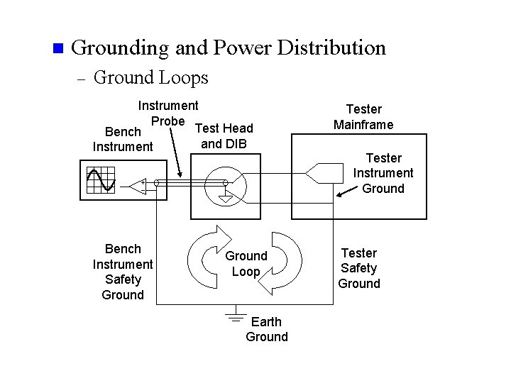
n Grounding and Power Distribution – Ground Loops Instrument Probe Test Head Bench and DIB Instrument Bench Instrument Safety Ground Loop Earth Ground Tester Mainframe Tester Instrument Ground Tester Safety Ground
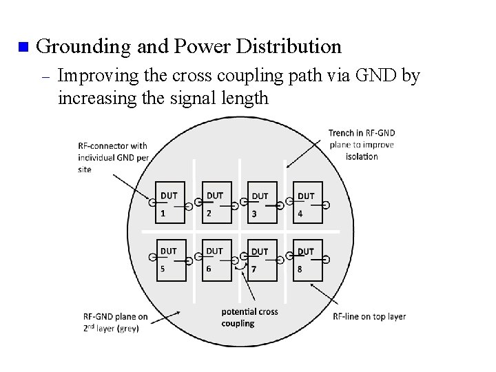
n Grounding and Power Distribution – Improving the cross coupling path via GND by increasing the signal length
n DIB Components – DUT Sockets and Contactor Assemblies n The DUT pins and the circuit traces on a DIB must be connected temporarily during test program execution. A hand-test socket or a handler contactor assembly makes the temporary connection. The most important thing to note is that the metallic contacts of the socket or contactor assembly represent an extra resistance, inductance, and capacitance to ground that will not exist when the DUT is soldered directly to the PCB in the customer’s system-level application. n Sometimes the parasitic elements are unimportant to a device’s operation, but other times, particularly at high frequencies, they can be extremely critical.
n DIB Components – Contact Pads, Pogo Pins, and Socket Pins n Contact pads are metal pads formed on the outer trace layers of a DIB PCB. They appear on DIB schematics as circles, black dots, or connector bars. These pads allow a relatively non-abrasive connection between one layer of interface hardware and the next. Two common uses for connector pads are pogo pin connections and DUT socket pin or contactor pin connections. A pogo pin is a spring-loaded gold-plated rod that provides a connection between two connector pads. Pogo pins may have blunted ends, pointed ends, or crown-shaped ends, depending on the connection requirements. Pointed or crown-shaped ends tend to dig into the pad surface, providing a reliable, low resistance connection to the pad. However, the digging action may eventually destroy the pad. Blunted pogo pins are less abrasive to the pads, but are slightly less reliable since they don’t dig into the pad surface.
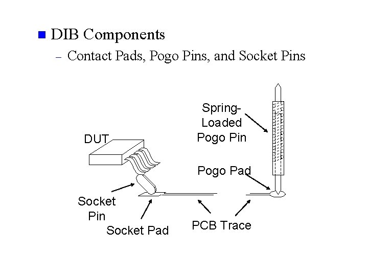
n DIB Components – Contact Pads, Pogo Pins, and Socket Pins DUT Spring. Loaded Pogo Pin Pogo Pad Socket Pin Socket Pad PCB Trace
n DIB Components – Contact Pads, Pogo Pins, and Socket Pins n A connection formed with a contact pad can be treated as an ideal zero impedance connection in most cases. n Pogo pins and socket pins also add inductance to the signal path. The inductance may be as little as one n. H or as large as a few tens of n. H. In general, long thin pins add more inductance than short fat ones. Socket pins and pogo pins may also introduce pin-to-pin or pin-to-ground parasitic capacitance on the order of a few p. F. n You seldom can control the size of the current loop, therefore you are basically left with selecting the appropriate socket with short pins.
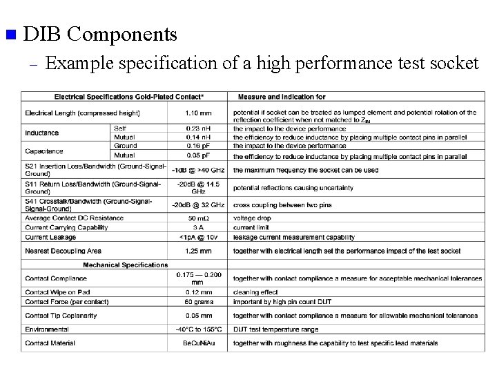
n DIB Components – Example specification of a high performance test socket

n DIB Components – Electromechanical Relays n n One of the more common DIB components used in mixed-signal testing is the electromechanical relay. The relay is an electromagnetically controlled mechanical switch. Relays allow the DIB circuits to be appropriately reconfigured for each measurement in the test program. As one of the few moving parts on a DIB, relays represent a potential reliability problem in production. The metal contacts in a relay are pulled open or closed using an electromagnetic field generated by a DC current passing through a coil of wire. The current is switched on or off under test program control as the test code is executed. Flyback diodes are sometimes added to the DIB in parallel with each relay coil to prevent the coil’s inductive kickback voltage from damaging the current-driving electronics located inside the tester.
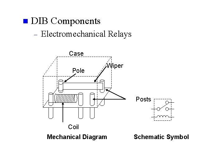
n DIB Components – Electromechanical Relays Case Pole Wiper Posts Coil Mechanical Diagram Schematic Symbol
n DIB Components – Electromechanical Relays n n In conventional relays, the moving armature is called the wiper. Since it pivots on its pole, it may eventually wear out and get stuck. A more reliable relay is the reed relay, which uses two springy metal reeds that become magnetized by the coil’s electromagnetic field. They are attracted to each other by the induced magnetism. Since the reeds do not swing on any pivot, there are no parts to wear out other than the point of contact between the two reeds. Reed relays are used very often on DIBs because of their superior reliability. Damage can also be caused to the wiper and contacts by abrupt changes in the current passing through the contacts as they open and close. The high di/dt current changes can induce large inductive voltage spikes, leading to a spark that welds the contacts together.
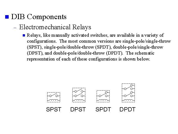
n DIB Components – Electromechanical Relays n Relays, like manually activated switches, are available in a variety of configurations. The most common versions are single-pole/single-throw (SPST), single-pole/double-throw (SPDT), double-pole/single-throw (DPST), and double-pole/double-throw (DPDT). The schematic representation of each of these configurations is shown below. SPST DPST SPDT DPDT
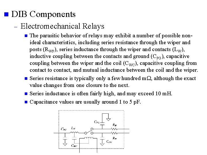
n DIB Components – Electromechanical Relays n n The parasitic behavior of relays may exhibit a number of possible nonideal characteristics, including series resistance through the wiper and posts (RWP), series inductance through the wiper and contacts (LW), inductive coupling between the contacts and ground (CPG), capacitive coupling between the wiper and the coil (CWC), capacitive coupling from contact to contact, and mutual inductance between the coil and the wiper. Series resistance is typically only a few hundred m , although the exact value changes from one closure to the next. Series inductance is often fairly high, and may exceed 10 m. H. Capacitance values are usually around 1 to 5 p. F.
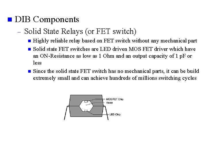
n DIB Components – Solid State Relays (or FET switch) n n n Highly reliable relay based on FET switch without any mechanical part Solid state FET switches are LED driven MOS FET driver which have an ON-Resistance as low as 1 Ohm and an output capacity of 1 p. F or less Since the solid state FET switch has no mechanical parts, it can be build extremely small and can achieve hundreds of millions switching cycles
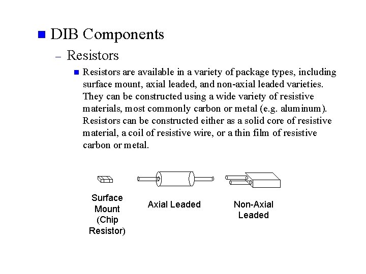
n DIB Components – Resistors n Resistors are available in a variety of package types, including surface mount, axial leaded, and non-axial leaded varieties. They can be constructed using a wide variety of resistive materials, most commonly carbon or metal (e. g. aluminum). Resistors can be constructed either as a solid core of resistive material, a coil of resistive wire, or a thin film of resistive carbon or metal. Surface Mount (Chip Resistor) Axial Leaded Non-Axial Leaded
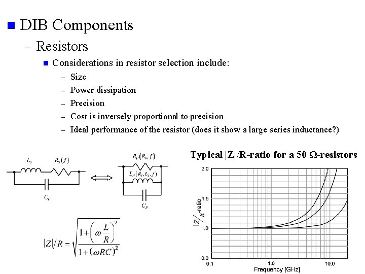
n DIB Components – Resistors n Considerations in resistor selection include: – – – Size Power dissipation Precision Cost is inversely proportional to precision Ideal performance of the resistor (does it show a large series inductance? ) Typical |Z|/R-ratio for a 50 Ω-resistors
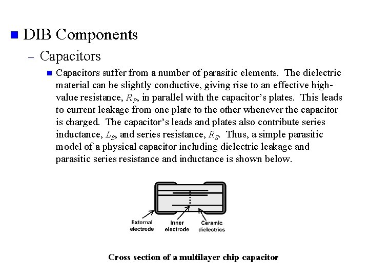
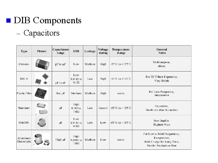
n DIB Components – Capacitors n Capacitors suffer from a number of parasitic elements. The dielectric material can be slightly conductive, giving rise to an effective highvalue resistance, RP, in parallel with the capacitor’s plates. This leads to current leakage from one plate to the other whenever the capacitor is charged. The capacitor’s leads and plates also contribute series inductance, LS, and series resistance, RS. Thus, a simple parasitic model of a physical capacitor including dielectric leakage and parasitic series resistance and inductance is shown below. Cross section of a multilayer chip capacitor
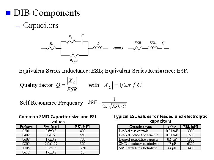
n DIB Components – Capacitors Equivalent Series Inductance: ESL; Equivalent Series Resistance: ESR Quality factor with Self Resonance Frequency Common SMD Capacitor size and ESL values Package 0201 0402 0603 0805 1206 0612 Size [mm] 0. 6 x 0. 3 1 x 0. 5 1. 6 x 0. 8 2. 0 x 1. 25 3. 2 x 1. 6 x 3. 2 ESL [p. H] 400 550 700 800 1250 63 Typical ESL values for leaded and electrolytic capacitors Capacitor type Leaded disc ceramic Leaded monolithic ceramic SMD aluminum electrolytic SMD tantalum electrolytic value 0. 01 m. F 0. 1 m. F 47 m. F ESL [p. H] 3000 1600 1900 6800 3400
n DIB Components – Capacitors
n DIB Components – Inductors and Ferrite Beads n Inductor are occasionally required as part of a DUT circuit such as a voltage doubler. They may also be used as part of a passive load circuit that must be connected to a DUT output to simulate a speaker coil or similar systemlevel component. Inductors can also be used in conjunction with capacitors to simulate long transmission lines by building an LC network. Inductors are used as part of an RF matching circuit n Inductors can be modeled as an inductance in series with a resistance. n n n
n DIB Components – Inductors and Ferrite Beads n n n Depending on the magnetic core material chosen, the inductor may also exhibit lossy behavior at high frequencies, resulting in an apparent increase in the series resistance of the coil wire. In fact, a class of inductors called ferrite beads are intentionally designed with very lossy core materials to achieve a component with near-zero resistance at low frequencies and higher resistance at higher frequencies. Ferrite beads are useful for blocking high frequency interference signals. They can reduce AC crosstalk from one circuit to another, while allowing DC current to flow freely.
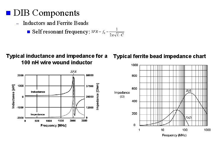
n DIB Components – Inductors and Ferrite Beads n Self resonant frequency: Typical inductance and impedance for a Typical ferrite bead impedance chart 100 n. H wire wound inductor
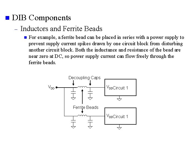
n DIB Components – Inductors and Ferrite Beads n For example, a ferrite bead can be placed in series with a power supply to prevent supply current spikes drawn by one circuit block from disturbing another circuit block. Both the inductance and resistance of the bead are near zero at DC, so power supply current can flow freely through the ferrite beads. Decoupling Caps VDDCircuit 1 Ferrite Beads VDDCircuit 1
n DIB Components – Transformers and Power Splitters n n n Transformers are sometimes used on DIBs to translate a high-frequency single-ended signal into a differential signal or vice-versa. Unfortunately, the transformer’s frequency response is highly dependent on the output impedance of the transmitting circuit as well as the input impedance of the receiving circuit. Consequently, the frequency response of the transformer is difficult to accurately calibrate, since it may change from one DUT to the next.
n DIB Components – Transformers and Power Splitters n n n Power splitters are controlled impedance transformers that are useful at high frequencies. They are typically used in RF and microwave systems, but occasionally find use on mixed-signal DIBs. Power splitter and transformer operation are sometimes limited to a small range of frequencies depending on the internal circuits Transformers and power splitters, by contrast, present a low impedance inductive or resistive load the DUT. Since many DUTs can’t drive low impedances, transformers and power splitters are often unusable. However, because they can handle frequencies well above those handled by active op amp circuits, they are sometimes the only viable choice
n DIB Components – – – Matching Circuits for RF Boards The term matching means the impedance transformation, in terms of ATE it means in the most cases to transform the input impedance of the DUT to the port impedance of the ATE which his in most cased 50. In principle there kinds of matching 1. 2. 3. The conjugate Match transforms the load impedance ZL to the conjugate match of the source impedance ZS with ZS = ZL*. This type of matching will maximize the power delivery to the load, but will not minimize the reflections unless ZS is real. The load match transforms the load impedance ZL to the line impedance Z 0. This matching is minimizing the reflections but does not maximize the delivered power unless Z 0 is real. The load matching is best used at ends of transmission lines. The functional match which will load the device with an impedance that optimize the performance. This match is done e. g. when optimizing the noise figure of an LNA since the best noise performance does not require necessarily the same load impedance than the best gain or power performance.
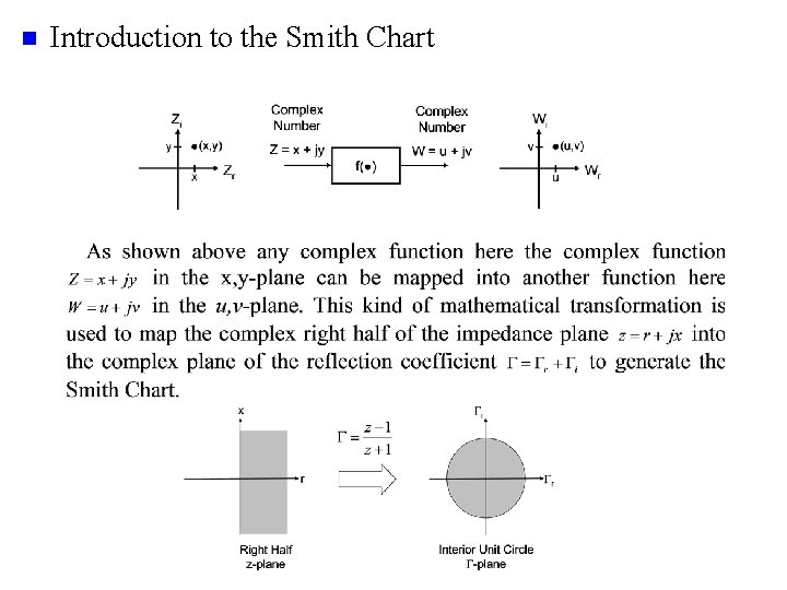
n Introduction to the Smith Chart
n Common DIB Mistakes – Poor Power Supply and Ground Layout n n n One of the most common sources of noise injection in mixed-signal DIBs is poor power and ground layout. The best way to avoid problems with power distribution and grounding is to use as many planes as needed, without regard to DIB cost. Although each layer in a multilayer DIB adds fabrication cost, the expense is fairly negligible compared to the production yield loss due to poor DIB performance. A good DIB should include: – – one or two layers dedicated to digital transmission line ground and noisy current returns, one layer dedicated to analog current returns, one layer dedicated to low-current analog ground at least one layer dedicated to split power planes.
n Common DIB Mistakes – Crosstalk n n n Another common problem on mixed-signal DIBs is crosstalk, especially between digital and analog signal lines. The digital-to-analog crosstalk problem can be reduced by placing analog signals on a separate layer from digital signals, with an analog ground plane between the two layers. Sensitive nodes should be as short as possible to avoid crosstalk and coupling of external noise sources. One of the most common sensitive nodes on a mixed-signal DUT is its current reference input. This input is typically tied to VDD or ground through a very high impedance bias resistor. The node between the bias resistor and the DUT is an extremely sensitive one. Noise injected into this node will translate directly into noise throughout the DUT. Therefore current bias nodes should always be kept extremely short, preferably surrounded by a shield ring.
n Common DIB Mistakes – Transmission Line Discontinuities Small discontinuities in transmission lines can lead to glitches on the rising and falling edges of very fast digital signals. n Such glitches can sometimes lead to timing errors or double clocked logic in the DUT. n The discontinuities are caused by lumped capacitance or inductance at transition points along the transmission line. For example, a lumped capacitance and/or inductance exists whenever a digital signal trace is routed between layers through a via or other through hole. n Avoid routing digital signals from one layer to another, unless absolutely necessary. n
n Common DIB Mistakes – Resistive Drops in Circuit Traces n n Even relatively short traces may have a series resistance of several hundred milliohms. If we try to force current through such a trace, we will get a voltage drop due to the parasitic resistance of the trace. Sometimes these voltage drops are unimportant, but other times they can lead to errors nearly as large as the parameter we are trying to measure. If the series resistance is serious enough to cause a problem, the trace can either be made wider, or a sensing circuit such as a Kelvin connection can be used to compensate for the resistive drops in the PCB trace.
n Common DIB Mistakes – Tester Instrument Parasitics n n The various cables and wires that connect a DUT to a tester’s instruments can present a significant capacitive load to the DUT’s pins. Often, the loading is high enough to cause gain errors, phase shifts, or even DUT circuit oscillations. It is very important for a test engineer to ask the design engineer responsible for each DUT circuit what its capacitive drive capabilities will be. If the output impedance of the DUT is incompatible with the tester’s load capacitance, then a voltage follower will probably be needed on the DIB buffer the DUT’s output.
n Common DIB Mistakes – Oscillations in Active Circuits n Operational amplifiers used in buffer amplifiers or other DIB circuits may break into oscillations if they are not laid out properly. – n For example, the inverting and non-inverting inputs to an op amp are extremely sensitive to parasitic capacitance. If these traces are laid out so that they are more than a few tenths of an inch long, the amplifier will often break into oscillations. Another source of oscillations is poor power supply and decoupling capacitor layout. Decoupling capacitors in general should always be placed very close to their supply pin.
n Common DIB Mistakes – Poor DIB Component Placement and PCB Layout n n n The physical layout of the DIB is extremely critical to mixed-signal DUT performance. Short traces have less parasitic resistance, inductance, and capacitance than long traces. The best way to achieve short PCB traces is to arrange the DIB components in a way that allows short traces, especially in critical nodes. Component placement, power and ground schemes, trace layout, and other physical decisions must be made with knowledge of the DUT and DIB circuits and their required performance.
n Summary A good DIB is one of the most critical elements in a successful mixed-signal test solution. Without good DIB performance, the DUT may be unable to meet its specifications, regardless of the quality of the test code. Many things lead to good mixed-signal DIB design, including proper component selection and placement, proper power and ground layout, proper PCB stackup, and proper attention to parasitic components related to PCB traces and DIB components. n It is critical for the test engineer to review his test plan and DIB design with the design engineers before the DIB is laid out and fabricated. Otherwise, the DIB may turn out to be an expensive but useless piece of test hardware, proving once again that concurrent engineering is critical to mixed-signal product development. n
- Slides: 108