Chapter 14 Optical Properties of Materials A ELECTROMAGNETIC


 where T, A, and R")

 h: Planck’s")


 Io and")


 for which absorption of visible light is")


 has a band gap of about 2. 4")


 that")
White light LED Lighting (b)Back light source of flat panel display LED")
 l. Oxides (conventional): • Y 2")
 Fig 6 l")
 light absorption, (2) vibrational relaxation,")
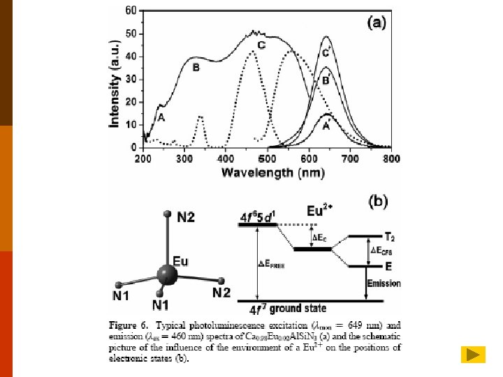
 649 nm) and emission (ìex ) 460 nm) spectra")
- Slides: 36
Chapter 14 Optical Properties of Materials
A. ELECTROMAGNETIC RADIATION F 21. 1 F 21. 2 In the classical sense, electromagnetic radiation is considered to be wave-like(wave), consisting of electric and magnetic field components that are perpendicular to each other and also to the direction of propagation. All electromagnetic radiation traverses a vacuum at the same velocity, namely, 3× 10⁸ m/s. This velocity, c, is related to the electric permittivity of vacuum Є0 and the magnetic permeability of a vacuum 0 through (21. 1) (21. 2 ) Frequency: hertz (Hz), and 1 Hz=1 cycle per second
From a quantum-mechanical perspective, rather than consisting of waves, radiation composed of groups or packets of energy, which are called photons(particle). Energy E of a photon. (21. 3) h: Planck’s constant, 6. 63× 10 -34 J-s B. LIGHT LINTERACTIONS WITH SOLIDS When light proceeds from one medium into another, the intensity I 0 of the beam incident equal the sum of the intensities of the transmitted absorbed, and reflected beams, denoted as IT, I A and IR I 0 = I T + I A+ I R (21. 4)
Radiation intensity: watts per square meter T+A+R=1 (21. 5) where T, A, and R represent, (IT/I 0), (IA/I 0), (IR/I 0). Transparent: transmitting light with relatively little absorption and reflection Translucent: light is transmittd diffusely; light is scattered within the interior, to the degree that objects are not clearly distinguishable. Opaque: impervious to the transmission of visible light
bulk metals: opaque throughout the entire visible spectrum; all light radiation is either absorbed or reflected. Electrically insulating materials: can be made to be transparent. Semiconducting materials: transparent or opaque. C. ATOMIC AND ELECTRONIC INTERACTIONS C-1. ELECTRONIC POLARIZATION A rapidly fluctuating electric field interacts to induce electronic poarization, or to shift the electron cloud relative to the nucleus of the atom. Two consequences: (1) some of the radiation energy may be absorbed, and (2) light waves are retarded in speed(refraction).
C-2. ELECTON TRANSITIONS For an isolated atom F 21. 3 (21. 6) h: Planck’s constant • the energy states for the atom are discrete, only specific ΔE’s exist between the energy levels; only photons of frequencies corresponding to the possible ΔE’s for the atom can be absorbed by electron transitions. • all of a photon’s energy is absorbed in each excitation event. • stimulated electron cannot remain in an excited state indefinitely; after a short time, it falls or decays back into its ground state (or unexcited level) • for solid materials: electron band structure
C-3. OPTICAL PROPERTIES OF METALS F 18. 4 F 21. 4 Metals are opaque because the incident radiation having frequencies within the visible range excites electrons into unoccupied energy states above the Fermi energy. incident radiation is absorbed Within a very thin outer layer, usually less than 0. 1 m (only metallic films thinner than 0. 1 m are capable of transmitting visible light. ). Metals are opaque to all electromagnetic radiation, from radio waves, into about the middle of the ultraviolet radiation. (Metals are transparent to high frequency (x-and r-ray) radiation. ) metals
Most of the absorbed radiation is reemitted from the surface in the form of visible light of the same wavelength, which appears as reflected light. The reflectivity for most metals is between 0. 90 and 0. 95; some small fraction of the energy from electron decay processes is dissipated as heat. The perceived color is determined by the wavelength distribution of the radiation that is reflected. A bright silvery appearance when exposed to white light indicates that the metal is highly reflective over the entire range of the visible spectrum, e. g. , aluminum and silver. Copper and gold appear red-orange and yellow: some of the energy associated with light photons having short wavelengths is not reemitted as visible light.
C-4. OPTICAL PROPERTIES OF NONMETALS F 18. 4 Nonmetallic materials may be transparent to visible light: reflection, absorption, refraction and transmission. D. REFRACTION T 21. 1 Index of refraction n: the ratio of the velocity in a vacuum c to the velocity in the medium v, (21. 7 ) The magnitude of n depends on the wavelength of the light. (Thus, e. g. , dispersion or separation of a beam of white light by a glass prism. ) (21. 1) (21. 8)
Є and : permittivity and permeability of the particular substance. (21. 9) Io and IR : intensities of the incident and reflected beams, if the light is normal (or perpendicular) to the interface Єr, r: dielectric constant and the relative magnetic permeabilety, since most substances are only slightly magnetic, r 1, (21. 10)
The retardation of electromagnetic radiation in a medium results from electronic polarization: generally, the larger an atom or ion, the greater will be the electronic polarization, the slower the velocity, and the greater the index of refraction. Index of refraction for soda-lime glass: 1. 5; Highly leaded glasses containing 90 wt% Pb. O: 2. 1. crystalline ceramics that have cubic crystal structures, and for glasses, the index of refraction is independent of crystallographic direction (i. e. , it is isotropic). Nocubic crystals, have an anisotropic n; the index is greatest along the directions that have the highest density of ions.
E. REFLECTION When light radiation passes from one medium into another having a different index of refraction, some of the light is scattered at the interface reflectivity R (21. 11) Io and IR : intensities of the incident and reflected beams, if the light is normal (or perpendicular) to the interface (21. 12)
n 1 and n 2 : indices of refraction of the media. If the incident light is not normal to the interface, R will depend on the angle of incidence. When light is transmitted from a vacuum or air into a solid s (21. 13 ) The index of refraction of air is very nearly unity. The higher the index of refraction of the solid, the greater is the reflectivity. The reflectivity vary with wavelength. Reflection losses for lenses and other optical instruments are minimized significantly by coating the reflecting surface with very thin layers of dielectric materials such as magnesium fluoride (Mg. F 2).
F. ABSORPTION F 21. 5 Nonmetallic materials may be opaque or transparent to visible light; and, if transparent, they often appear colored. Light radiation is absorbed by two basic mechanisms: • electronic polarization (Section 21. 4): important only at light frequencies in the vicinity of the relaxation frequency of the constituent atoms. • valence band-conduction band electron transitions: depends on the electron energy band structure. absorption of a photon of light by the promotion or excitation of an electron from the nearly filled valence band, across the band gap, and into an empty state within the conduction band. hc >Eg hν>Eg (21. 14) (21. 15) λ
The maximum band gap energy Eg (max) for which absorption of visible light is possible semiconductor (21. 16 a ) F 21. 5 No visible light is absorbed by nonmetallic materials having band gap energies greater than about 3. 1 e. V; these materials, if of high purity, will appear transparent and colorless. The minimum band gap energy Eg (min) for which there is absorption of visible light is a ceramics
All visible light is absorbed for those semiconducting materials that have band gap energies less than about 1. 8 e. V; these materials are opaque. Only a portion of the visible spectrum is absorbed by materials having band gap energies between 1. 8 and 3. 1 e. V; consequently, these materials appear colored. Every nonmetallic material becomes opaque at some wavelength, which depends on the magnitude of its Eg. For example, diamond, having a band gap of 5. 6 e. V, is opaque to radiation having wavelengths less than about 0. 22 m.
If impurities or other electrically active defects are present, electron levels within the band gap may be introduced (such as the donor and acceptor levels (Section 18. 11), except that they lie closer to the center of the band gap), the electromagnetic energy that was absorbed by electron excitation must be dissipated, several mechanisms: • direct electron and hole recombination F 21. 5 (21. 17) • multiple-step electron transitions: one possibility, (Figure 21. 6 b) emission of two photons; alternatively, generation of a phonon (Figure 21. 6 c) F 21. 6
The intensity of transmitted or nonabsorbed radiation I’T continuously decreases with distance x (21. 18) I’ 0 : intensity of the nonreflected incident radiation. : absorption coefficient (in mm-1), Materials that have large values are considered to be highly absorptive. G. Transmission F 21. 7 (21. 19) It is assumed that the same medium exists outside both front and back faces. R, A, and T depends on light wavelength
H. COLOR F 21. 8 F 21. 9 Transparent materials appear colored, the color discerned is a result of the combination of wavelengths that are transmitted. If absorption is uniform for all visible wavelengths, the materials appears colorless; e. g. , high-purity inorganic glasses and high-purity and single-crystal diamonds and sapphire. Fraction of the visible light having energies greater than Eg is selectively absorbed (by valence band conduction band electron transitions. ) some of this absorbed radiation is reemitted as the excited electrons drop back into their original, lower-lying energy states. It is not necessary that this reemission occur at the same frequency as that of the absorption. As a result, for semiconducting materials the color depends on the frequency distribution of both transmitted and reemitted light beams.
Fro example, cadmium sulfide (Cd. S) has a band gap of about 2. 4 e. V; it absorbs blue and violet portions, some of this energy is reradiated as light having other wavelengths. Nonabsorbed visible light consists of photons having energies between about 1. 8 and 2. 4 e. V. Cadmium sulfide takes on a yelloworange color • Ceramics, specific impurities also introduce electron levels within the forbidden band gap, photons having energies less than the band gap may be emitted as a consequence of electron decay processes involving impurity atoms or ions. F 3. 17 F 20. 20
For example, high-purity and single-crystal aluminum oxide or sapphire is colorless. Ruby, which has a brilliant red color, is simply sapphire to which has been added 0. 5 to 2% of chromium oxide (Cr 2 O 3). Cr 3+ ion substitutes for the Al 3+ ion in the Al 2 O 3 crystal structure and introduces impurity levels within the wide energy band gap of the sapphire. Nonabsorbed or transmitted light mixed with reemitted light imparts to ruby its deep -red color. Inorganic glasses are colored by incorporating transition or rare earth ions while the glass is still in the molten state: blue-green; Co 2+ , blue-violet; Cr 3+, green; Mn 2+, yellow; and Mn 3+ , purple. These colored glasses are also used as glazes (釉料), decorative coatings (彩色鍍層) on ceramic ware (陶瓷器件).
I. OPACITY AND TRANSLUCENCY IN INSULATORS Many dielectric materials that are intrinsically transparent may be made translucent or even opaque because of interior reflection and refraction: multiple scattering events. Opacity results when the scattering is so F 21. 10 extensive. Internal scattering: • polycrystalline specimens in which the index of refraction is anisotropic normally appear translucent. Both reflection and refraction occur at grain boundaries. • scattering of light also occurs in two-phase materials • The greater difference in the refractive index difference, the
Residual porosity in the form of finely dispersed pores. Also effectively scatter light radiation. For intrinsic polymers (without additives and impurities), the degree of translucency is influenced primarily by the extent of crystallinity. Some scattering of visible light occurs at the boundaries between sperulites and between crystalline and amorphous regions, as a result of different indices of refraction. For highly crystalline specimens: translucency, even opacity. Highly amorphous polymers are completely transparent.
J. APPLICATIONS OF OPTICAL PROPERTIES J-1. LUMINESCENCE Some materials are capable of absorbing energy and then reemitting visible light in a phenomenon called luminescence. Energy is absorbed when an electron is promoted to an excited energy state; visible light is emitted when it falls back to a lower energy state if 1. 8 e. V<hv<3. 1 e. V. The absorbed energy may be supplied as higher-energy electromagnetic radiation (ultraviolet light) high energy electrons, or by heat, mechanical, or chemical energy. Luminescence is classified according to the delay time between absorption and reemission events.
If reemission occurs for times much less than one second: fluorescence; for longer times: phosphorescence; e. g. , sulfides, oxides, tungstates, and a few organic materials. Ordinarily, pure materials do not disply these phenomena, and to induce them, impurities in controlled concentrations must be added. Luminescence applications: • fluorescent lamps: glass housing, coated on the inside with tungstates or silicates. Ultraviolet light is generated from a mercury glow discharge, which causes the coating to fluoresce and emit white light.
• television screen: inside of the screen is coated with a material that fluoresces as an electron beam inside the picture tube very rapidly traverses the screen F 18. 19 • Detection of x-rays and υ-rays • light-emitting diodes(LEDs) : some p-n rectifying junctions, (Section 18. 15), may also be used to generate visible light: electroluminescence. Such diodes that luminesce visible light are the familiar light-emitting diodes(LEDs), which are used for digital displays. The characteristic color of an LED depends on the particular semiconducting material that is used. • White light LED Lighting: photoluminescence. #60 #2 #3 #4 #5 #24 Fig. 6 #25
J-2. PHOTOCONDUCTIVTTY The conductivity of semiconducting materials depends on: number of free electrons in the conduction band number of holes in the valence. Photon-induced electron transitions: when a specimen of a photoconductive materials is illuminated, the conductivity increases: photoconductivity. Applications: photographic light meters. (cadmium sulfide is commonly utilized) sunlight be directly converted into electrical energy solar cells, empoly semiconductors. Reverse of that for the light-emitting diode. A p-n junction is used in which potoexcited electrons and holes are drawn away from the junction, in opposite directions, and become part of an external current. Electron transitions heretofore discussed: spontaneous (without any external provocation. ) random times, incoherent.
Laser: coherent light generated by electron transitions initiated by an external stimulus. “laser” light amplification by stimulated emission of radiation. solid -state ruby laser. Ruby single crystal of Al 2 O 3 (sapphire) added of 0. 05% Cr 3+ ions. The ruby laser is in the form of a rod, the ends of which are flat, parallel, and highly polished. Both ends are silvered such that one is totally reflecting and the other partially transmitting. Photons of 0. 56 m from the xenon lamp excite electrons from the Cr 3+ ions into higher energy states. Some fall back directly; other electrons decay into a metastable intermediate state, where they may reside for up to 3 ms 3 ms is a relatively long time, a large number of these metatable states may become
B phosphors Excitation spectra of Ca. S: Eu Phosphor powders Blue LED chip Emission spectra of Ca. S: Eu
Ι. Introduction to Phosphors 01 A. Phosphors: luminescence conversion materials 02 material (powders) that emit visible light when irradiated with shorter wavelength light (UV or blue) Beta-Si. Al. ON: Eu Alpha-Si. Al. ON: Eu Ca. Si. Al. N 3: Eu
B. Applications (a)White light LED Lighting (b)Back light source of flat panel display LED For TV Backlight
C. Chemical Composition: Host Lattice : activator (doping) l. Oxides (conventional): • Y 2 O 3:Eu+3 • Y 3 Al 5 O 12:Ce+3 (YAG) • Tb 3 Al 5 O 12:Ce+3 l. Nitrides and Oxynitrides (newly developed): • Ca 2 Si 5 N 8:Eu+2 • Ca 2 Si 2 N 2 O 2:Eu+2 • Ca-α-Si. Al. ON:Eu+2 • Y-α-Si. Al. ON:Ce+3
D. Features of Nitride and Oxynitride Phosphors (compared to oxide phosphors) Fig 6 l Potential advantages • high thermal and chemical stability • high emission intensity (or high quantum yield) • long wavelength( orange-red) emission, improving color rendering index, which are usually difficult to be achieved by other phosphors. l. More difficult to be synthesized ․more severe synthesis conditions, e. g. , high reaction temperature, high N 2 pressure, long reaction time or use of moisture or oxygen sensitive starting materials.
Fundamentals of luminescence Fig. 2 The Jablonski diagram: (1) light absorption, (2) vibrational relaxation, (3) internal conversion (IC), (4) intersystem crossing (ISC), (5) radiative transition, and (6) nonradiative transition.
Typical photoluminescence excitation (ìmon ) 649 nm) and emission (ìex ) 460 nm) spectra of Ca 0. 98 Eu 0. 02 Al. Si. N 3 (a) and the schematic picture of the influence of the environment of a Eu 2+ on the positions of electronic states (b).