Chapter 11 PWM and DC Motor Control STM

- Slides: 20

Chapter 11: PWM and DC Motor Control STM 32 F 0 Arm Cortex M 0 Programming for Embedded Systems Using C Language with STM 32 F 0 Nucleo Board by Mazidi, et al. www. microdigitaled. com

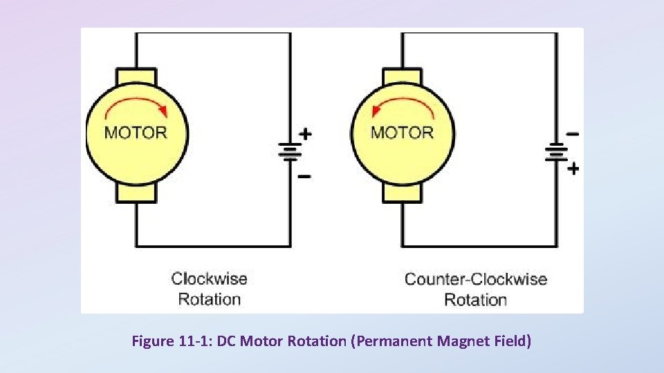
Figure 11 -1: DC Motor Rotation (Permanent Magnet Field)

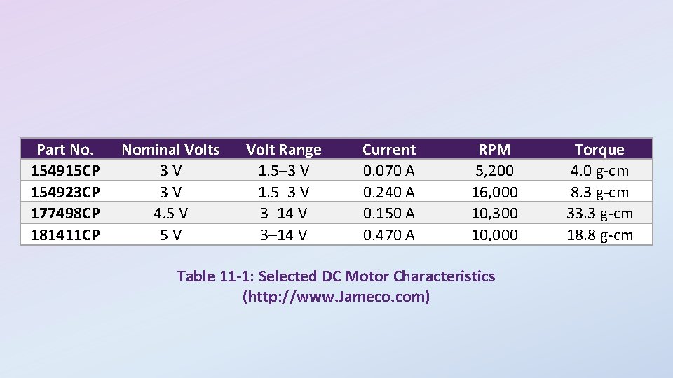
Part No. 154915 CP 154923 CP 177498 CP 181411 CP Nominal Volts 3 V 3 V 4. 5 V 5 V Volt Range 1. 5– 3 V 3– 14 V Current 0. 070 A 0. 240 A 0. 150 A 0. 470 A RPM 5, 200 16, 000 10, 300 10, 000 Table 11 -1: Selected DC Motor Characteristics (http: //www. Jameco. com) Torque 4. 0 g-cm 8. 3 g-cm 33. 3 g-cm 18. 8 g-cm

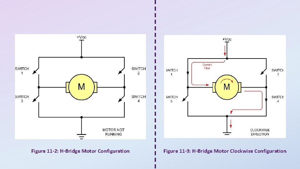
Figure 11 -2: H-Bridge Motor Configuration Figure 11 -3: H-Bridge Motor Clockwise Configuration

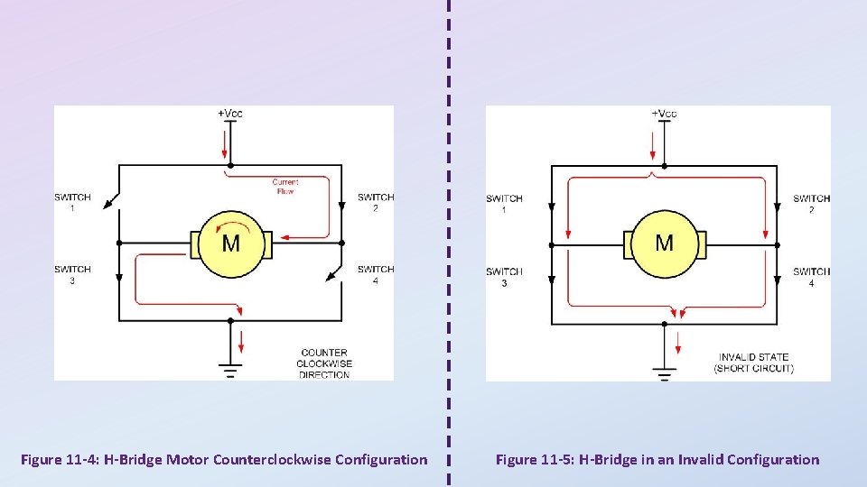
Figure 11 -4: H-Bridge Motor Counterclockwise Configuration Figure 11 -5: H-Bridge in an Invalid Configuration

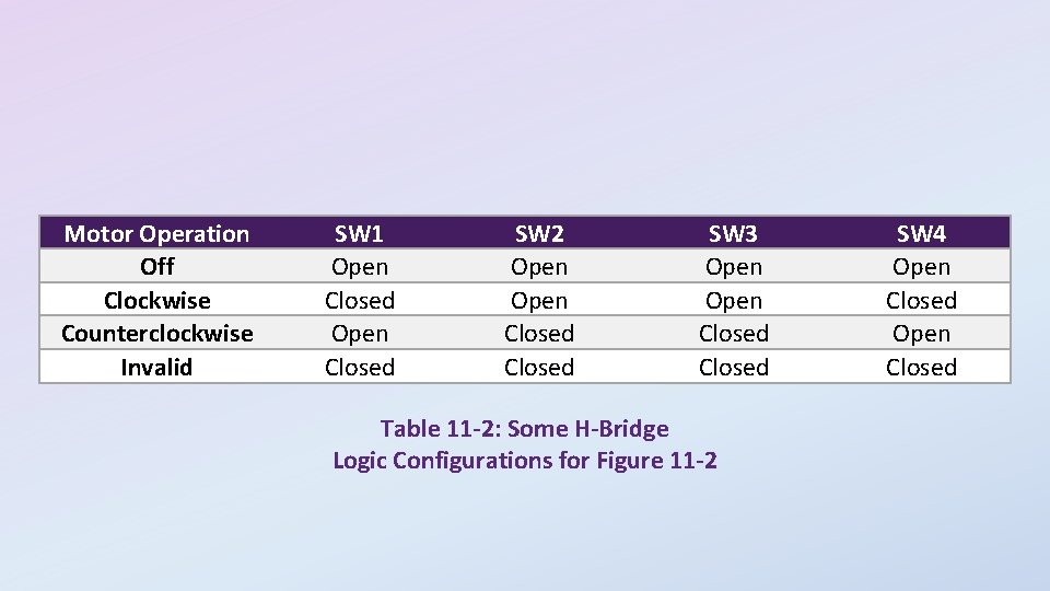
Motor Operation Off Clockwise Counterclockwise Invalid SW 1 Open Closed SW 2 Open Closed SW 3 Open Closed Table 11 -2: Some H-Bridge Logic Configurations for Figure 11 -2 SW 4 Open Closed

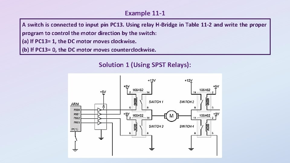
Example 11 -1 A switch is connected to input pin PC 13. Using relay H-Bridge in Table 11 -2 and write the proper program to control the motor direction by the switch: (a) If PC 13= 1, the DC motor moves clockwise. (b) If PC 13= 0, the DC motor moves counterclockwise. Solution 1 (Using SPST Relays):

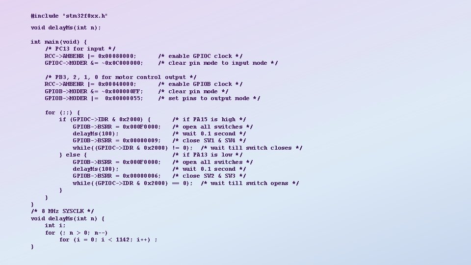
#include "stm 32 f 0 xx. h" void delay. Ms(int n); int main(void) { /* PC 13 for input */ RCC->AHBENR |= 0 x 00080000; GPIOC->MODER &= ~0 x 0 C 000000; /* enable GPIOC clock */ /* clear pin mode to input mode */ /* PB 3, 2, 1, 0 for motor control output */ RCC->AHBENR |= 0 x 00040000; /* enable GPIOB clock */ GPIOB->MODER &= ~0 x 000000 FF; /* clear pin mode */ GPIOB->MODER |= 0 x 00000055; /* set pins to output mode */ for (; ; ) { if (GPIOC->IDR & 0 x 2000) { GPIOB->BSRR = 0 x 000 F 0000; delay. Ms(100); GPIOB->BSRR = 0 x 00000009; while((GPIOC->IDR & 0 x 2000) } else { GPIOB->BSRR = 0 x 000 F 0000; delay. Ms(100); GPIOB->BSRR = 0 x 00000006; while((GPIOC->IDR & 0 x 2000) } } } /* 8 MHz SYSCLK */ void delay. Ms(int n) { int i; for (; n > 0; n--) for (i = 0; i < 1142; i++) ; } /* /* != /* /* == if PA 15 is high */ open all switches */ wait 0. 1 second */ close SW 1 & SW 4 */ 0); /* wait till switch closes */ if PA 13 is low */ open all switches */ wait 0. 1 second */ close SW 2 & SW 3 */ 0); /* wait till switch opens */

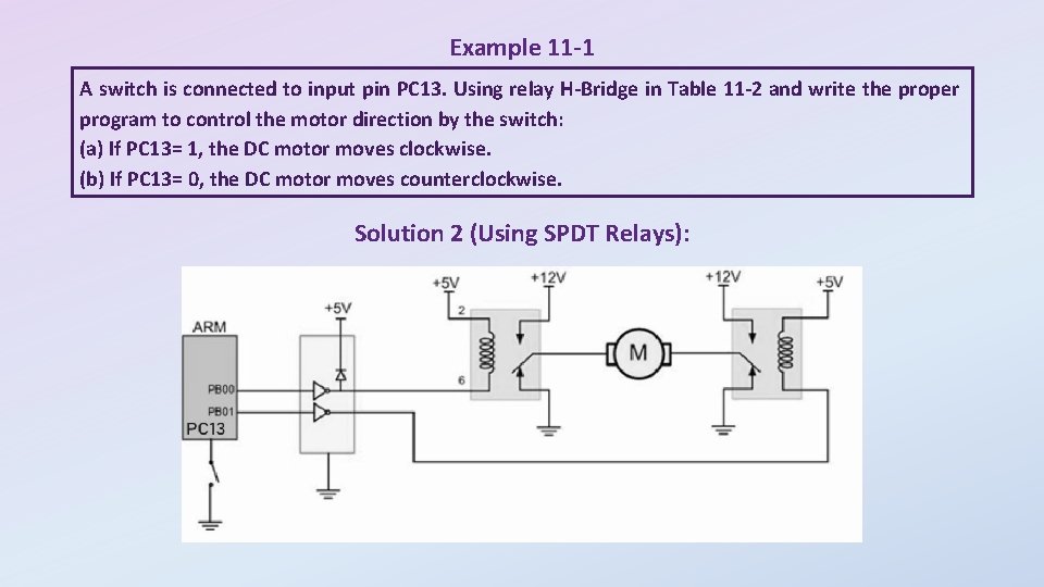
Example 11 -1 A switch is connected to input pin PC 13. Using relay H-Bridge in Table 11 -2 and write the proper program to control the motor direction by the switch: (a) If PC 13= 1, the DC motor moves clockwise. (b) If PC 13= 0, the DC motor moves counterclockwise. Solution 2 (Using SPDT Relays):

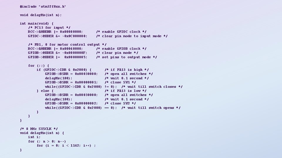
#include "stm 32 f 0 xx. h" void delay. Ms(int n); int main(void) { /* PC 13 for input */ RCC->AHBENR |= 0 x 00080000; GPIOC->MODER &= ~0 x 0 C 000000; /* enable GPIOC clock */ /* clear pin mode to input mode */ /* PB 1, 0 for motor control output RCC->AHBENR |= 0 x 00040000; /* GPIOB->MODER &= ~0 x 0000000 F; /* GPIOB->MODER |= 0 x 00000005; /* for (; ; ) { if (GPIOC->IDR & 0 x 2000) { GPIOB->BSRR = 0 x 00030000; delay. Ms(100); GPIOB->BSRR = 0 x 00000001; while((GPIOC->IDR & 0 x 2000) } else { GPIOB->BSRR = 0 x 00030000; delay. Ms(100); GPIOB->BSRR = 0 x 00000002; while((GPIOC->IDR & 0 x 2000) } } */ enable GPIOB clock */ clear pin mode */ set pins to output mode */ } /* 8 MHz SYSCLK */ void delay. Ms(int n) { int i; for (; n > 0; n--) for (i = 0; i < 1142; i++) ; } /* /* != /* /* == if PA 13 is high */ open all switches */ wait 0. 1 second */ close SW 1 */ 0); /* wait till switch closes */ if PA 13 is low */ open all switches */ wait 0. 1 second */ close SW 2 */ 0); /* wait till switch opens */

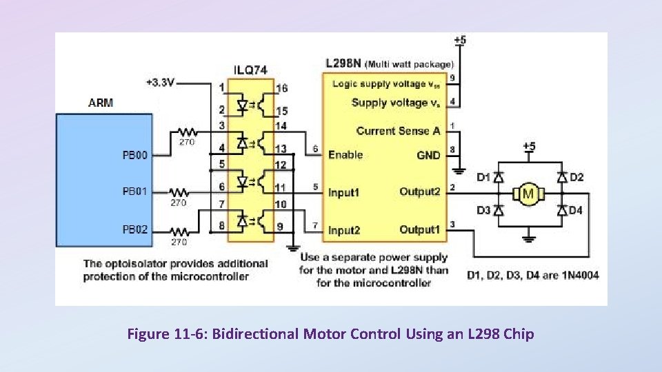
Figure 11 -6: Bidirectional Motor Control Using an L 298 Chip

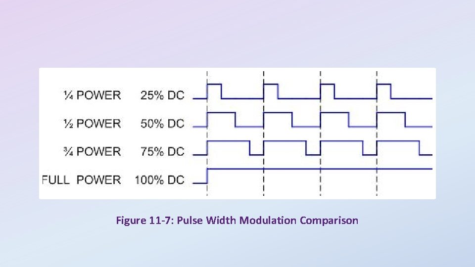
Figure 11 -7: Pulse Width Modulation Comparison

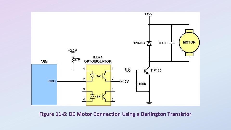
Figure 11 -8: DC Motor Connection Using a Darlington Transistor

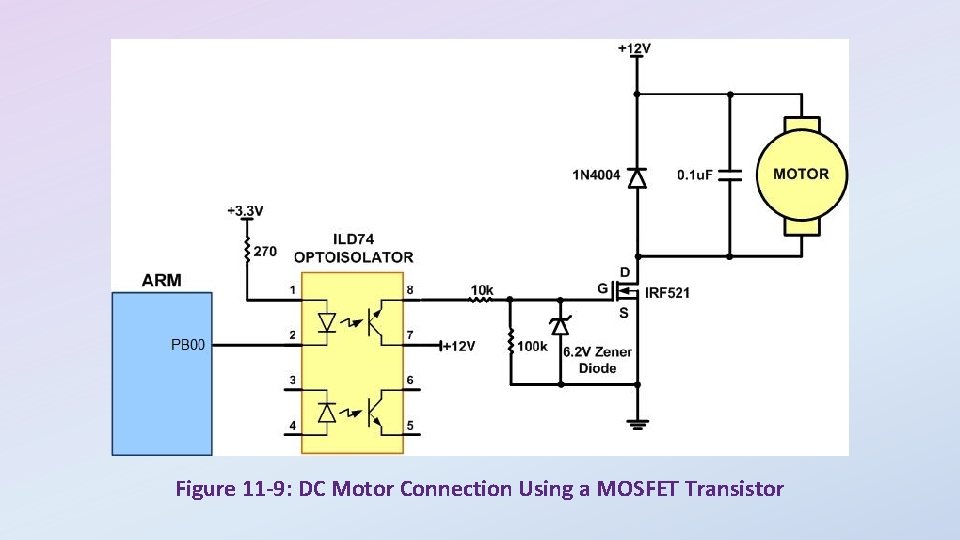
Figure 11 -9: DC Motor Connection Using a MOSFET Transistor

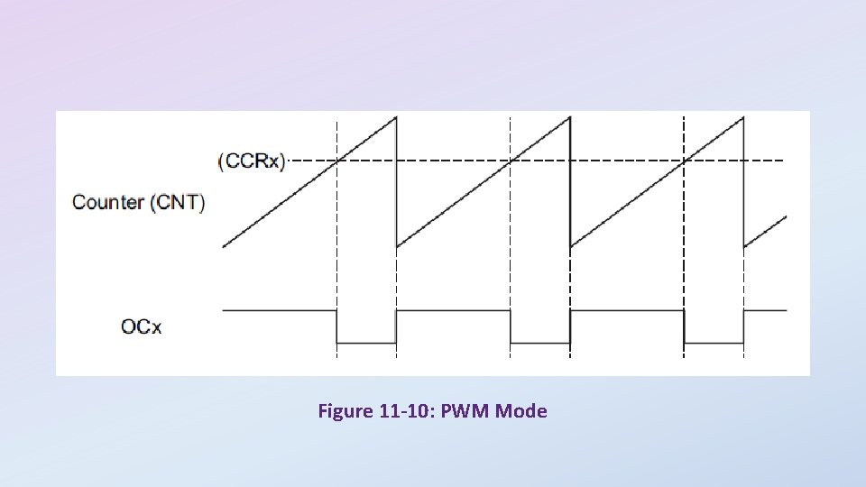
Figure 11 -10: PWM Mode

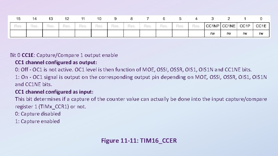
Bit 0 CC 1 E: Capture/Compare 1 output enable CC 1 channel configured as output: 0: Off - OC 1 is not active. OC 1 level is then function of MOE, OSSI, OSSR, OIS 1 N and CC 1 NE bits. 1: On - OC 1 signal is output on the corresponding output pin depending on MOE, OSSI, OSSR, OIS 1 N and CC 1 NE bits. CC 1 channel configured as input: This bit determines if a capture of the counter value can actually be done into the input capture/compare register 1 (TIMx_CCR 1) or not. 0: Capture disabled 1: Capture enabled Figure 11 -11: TIM 16_CCER

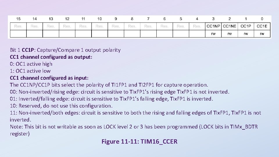
Bit 1 CC 1 P: Capture/Compare 1 output polarity CC 1 channel configured as output: 0: OC 1 active high 1: OC 1 active low CC 1 channel configured as input: The CC 1 NP/CC 1 P bits select the polarity of TI 1 FP 1 and TI 2 FP 1 for capture operation. 00: Non-inverted/rising edge: circuit is sensitive to TIx. FP 1's rising edge TIx. FP 1 is not inverted. 01: Inverted/falling edge: circuit is sensitive to TIx. FP 1's falling edge, TIx. FP 1 is inverted. 10: Reserved, do not use this configuration. 11: Non-inverted/both edges: circuit is sensitive to both the rising and falling edges of TIx. FP 1, TIx. FP 1 is not inverted. Note: This bit is not writable as soon as LOCK level 2 or 3 has been programmed (LOCK bits in TIMx_BDTR register) Figure 11 -11: TIM 16_CCER

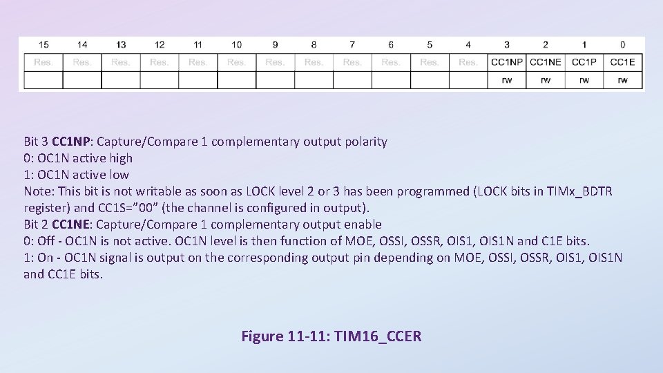
Bit 3 CC 1 NP: Capture/Compare 1 complementary output polarity 0: OC 1 N active high 1: OC 1 N active low Note: This bit is not writable as soon as LOCK level 2 or 3 has been programmed (LOCK bits in TIMx_BDTR register) and CC 1 S=” 00” (the channel is configured in output). Bit 2 CC 1 NE: Capture/Compare 1 complementary output enable 0: Off - OC 1 N is not active. OC 1 N level is then function of MOE, OSSI, OSSR, OIS 1 N and C 1 E bits. 1: On - OC 1 N signal is output on the corresponding output pin depending on MOE, OSSI, OSSR, OIS 1 N and CC 1 E bits. Figure 11 -11: TIM 16_CCER

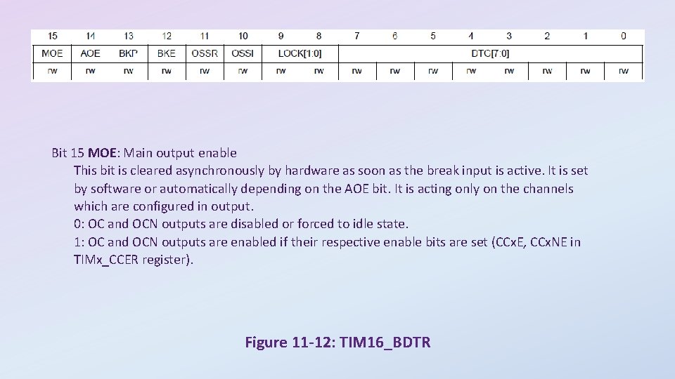
Bit 15 MOE: Main output enable This bit is cleared asynchronously by hardware as soon as the break input is active. It is set by software or automatically depending on the AOE bit. It is acting only on the channels which are configured in output. 0: OC and OCN outputs are disabled or forced to idle state. 1: OC and OCN outputs are enabled if their respective enable bits are set (CCx. E, CCx. NE in TIMx_CCER register). Figure 11 -12: TIM 16_BDTR

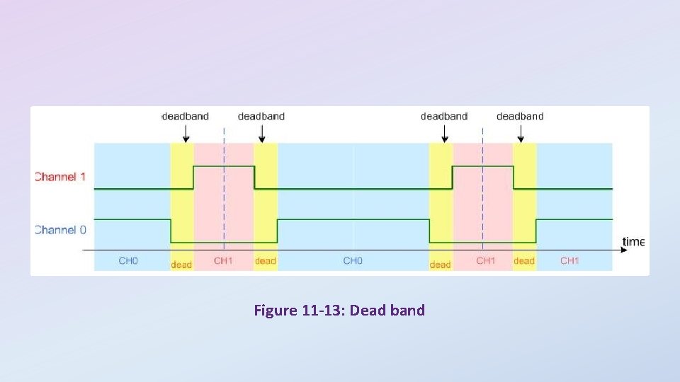
Figure 11 -13: Dead band