Chapter 1 SEMICONDUCTOR MATERIALS ELECTRONIC DEVICES EMT 1163

- Slides: 27

Chapter 1 SEMICONDUCTOR MATERIALS ELECTRONIC DEVICES EMT 116/3

CONTENT 1. 1 1. 2 1. 3 1. 4 1. 5 1. 6 1. 7 1. 8 1. 9 1. 10 Atomic structure Semiconductor, conductors and insulators Covalent bonding Conduction in semiconductors N-type and P-type semiconductors The diode Biasing the diode Voltage-current characteristic of a diode Diode models Testing a diode

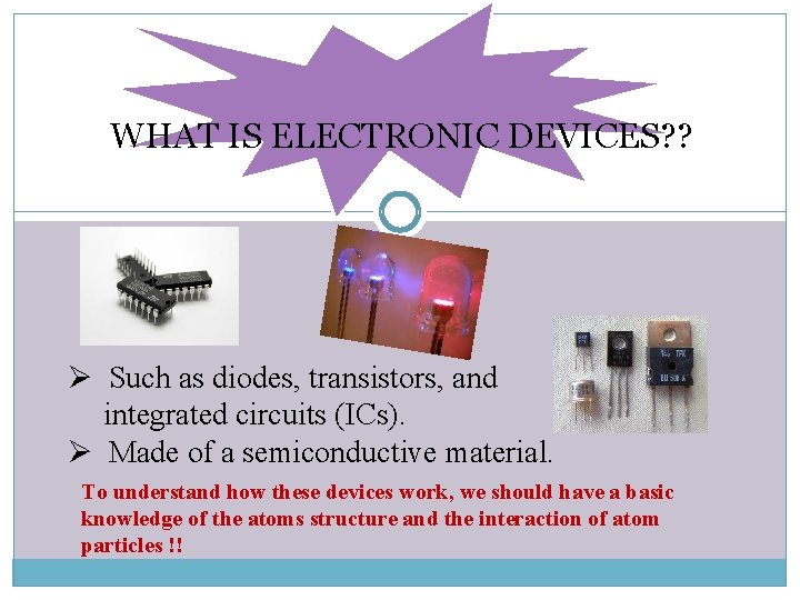
WHAT IS ELECTRONIC DEVICES? ? Ø Such as diodes, transistors, and integrated circuits (ICs). Ø Made of a semiconductive material. To understand how these devices work, we should have a basic knowledge of the atoms structure and the interaction of atom particles !!

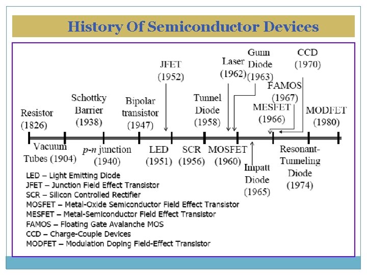
History Of Semiconductor Devices

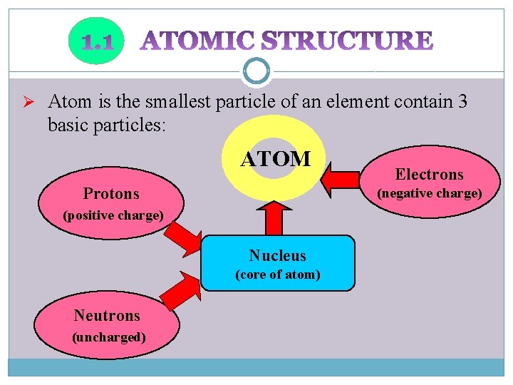
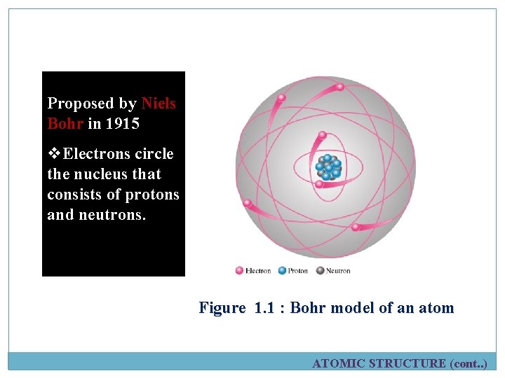
Ø Atom is the smallest particle of an element contain 3 basic particles: ATOM Protons (negative charge) (positive charge) Nucleus (core of atom) Neutrons (uncharged) Electrons

This model was Proposed by Niels Bohr in 1915 v. Electrons circle the nucleus that consists of protons and neutrons. Figure 1. 1 : Bohr model of an atom ATOMIC STRUCTURE (cont. . )

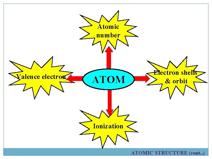
Atomic number Valence electron ATOM Electron shells & orbit Ionization ATOMIC STRUCTURE (cont. . )

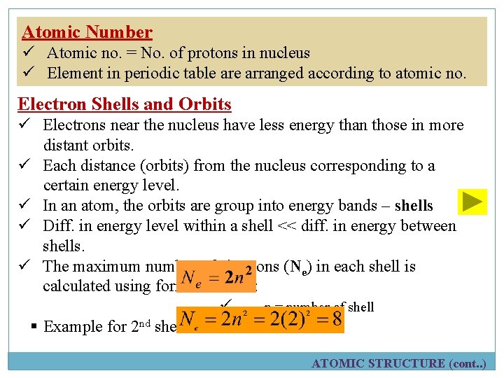
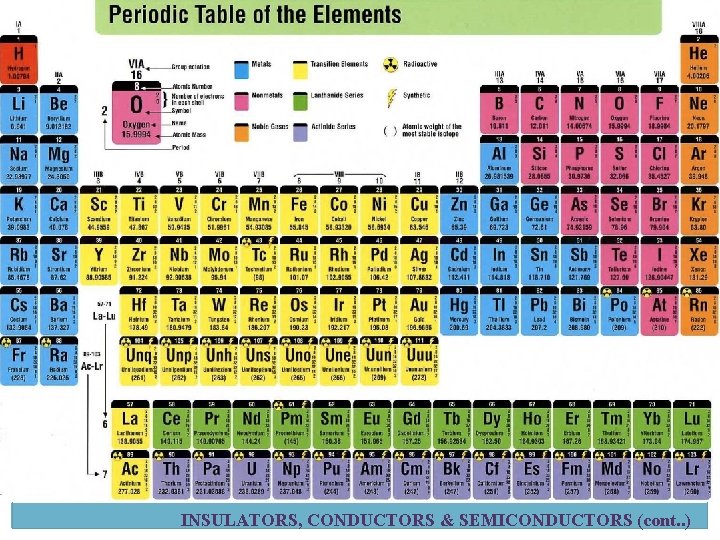
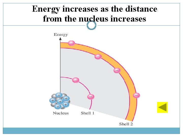
Atomic Number ü Atomic no. = No. of protons in nucleus ü Element in periodic table arranged according to atomic no. Electron Shells and Orbits ü Electrons near the nucleus have less energy than those in more distant orbits. ü Each distance (orbits) from the nucleus corresponding to a certain energy level. ü In an atom, the orbits are group into energy bands – shells ü Diff. in energy level within a shell << diff. in energy between shells. ü The maximum number of electrons (Ne) in each shell is calculated using formula below: ü n = number of shell § Example for 2 nd shell: ATOMIC STRUCTURE (cont. . )

INSULATORS, CONDUCTORS & SEMICONDUCTORS (cont. . )

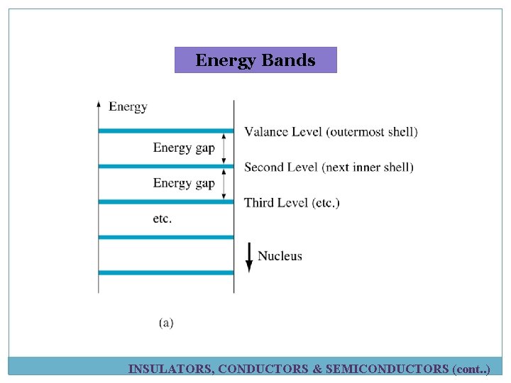
Energy increases as the distance from the nucleus increases

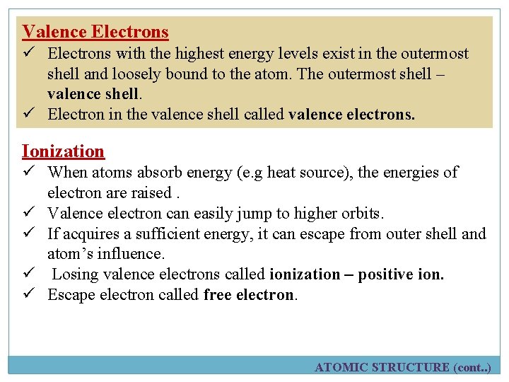
Valence Electrons ü Electrons with the highest energy levels exist in the outermost shell and loosely bound to the atom. The outermost shell – valence shell. ü Electron in the valence shell called valence electrons. Ionization ü When atoms absorb energy (e. g heat source), the energies of electron are raised. ü Valence electron can easily jump to higher orbits. ü If acquires a sufficient energy, it can escape from outer shell and atom’s influence. ü Losing valence electrons called ionization – positive ion. ü Escape electron called free electron. ATOMIC STRUCTURE (cont. . )

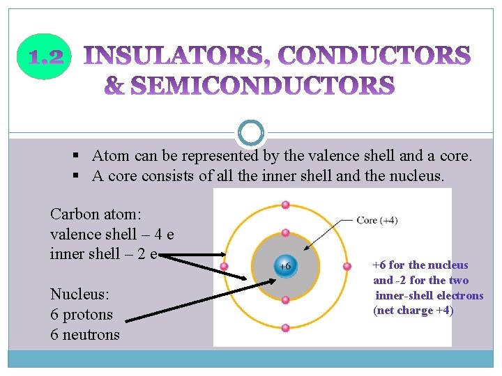
§ Atom can be represented by the valence shell and a core. § A core consists of all the inner shell and the nucleus. Carbon atom: valence shell – 4 e inner shell – 2 e Nucleus: 6 protons 6 neutrons +6 for the nucleus and -2 for the two inner-shell electrons (net charge +4)

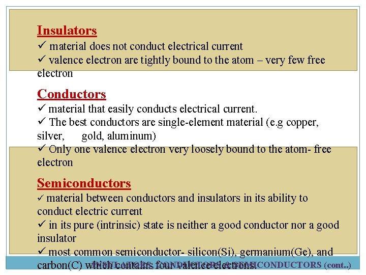
Insulators ü material does not conduct electrical current ü valence electron are tightly bound to the atom – very few free electron Conductors ü material that easily conducts electrical current. ü The best conductors are single-element material (e. g copper, silver, gold, aluminum) ü Only one valence electron very loosely bound to the atom- free electron Semiconductors ü material between conductors and insulators in its ability to conduct electric current ü in its pure (intrinsic) state is neither a good conductor nor a good insulator ü most common semiconductor- silicon(Si), germanium(Ge), and INSULATORS, CONDUCTORS & SEMICONDUCTORS (cont. . ) carbon(C) which contains four valence electrons.

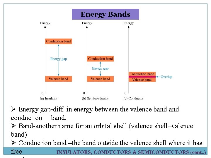
Energy Bands INSULATORS, CONDUCTORS & SEMICONDUCTORS (cont. . )

Energy Bands Ø Energy gap-diff. in energy between the valence band conduction band. Ø Band-another name for an orbital shell (valence shell=valence band) Ø Conduction band –the band outside the valence shell where it has free INSULATORS, CONDUCTORS & SEMICONDUCTORS (cont. . )

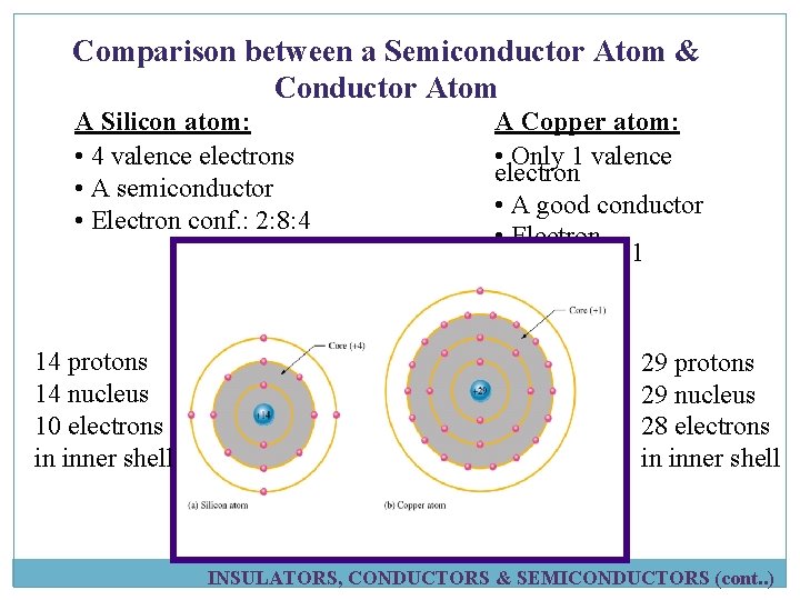
Comparison between a Semiconductor Atom & Conductor Atom A Silicon atom: • 4 valence electrons • A semiconductor • Electron conf. : 2: 8: 4 14 protons 14 nucleus 10 electrons in inner shell A Copper atom: • Only 1 valence electron • A good conductor • Electron conf. : 2: 8: 1 29 protons 29 nucleus 28 electrons in inner shell INSULATORS, CONDUCTORS & SEMICONDUCTORS (cont. . )

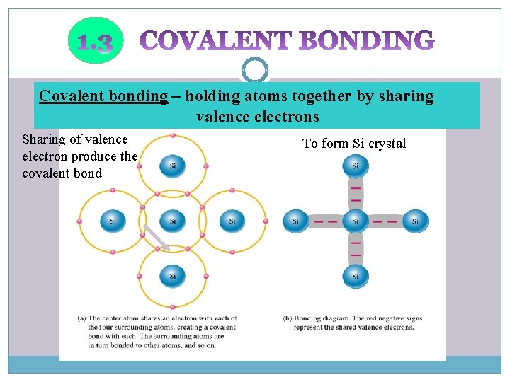
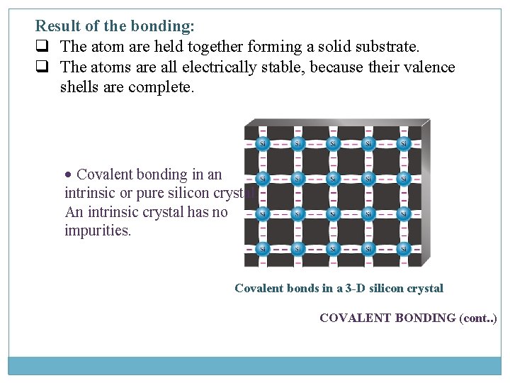
Covalent bonding – holding atoms together by sharing valence electrons Sharing of valence electron produce the covalent bond To form Si crystal

Result of the bonding: q The atom are held together forming a solid substrate. q The atoms are all electrically stable, because their valence shells are complete. • Covalent bonding in an intrinsic or pure silicon crystal. An intrinsic crystal has no impurities. Covalent bonds in a 3 -D silicon crystal COVALENT BONDING (cont. . )

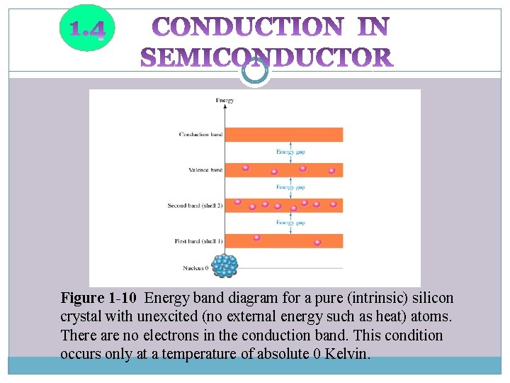
Figure 1 -10 Energy band diagram for a pure (intrinsic) silicon crystal with unexcited (no external energy such as heat) atoms. There are no electrons in the conduction band. This condition occurs only at a temperature of absolute 0 Kelvin.

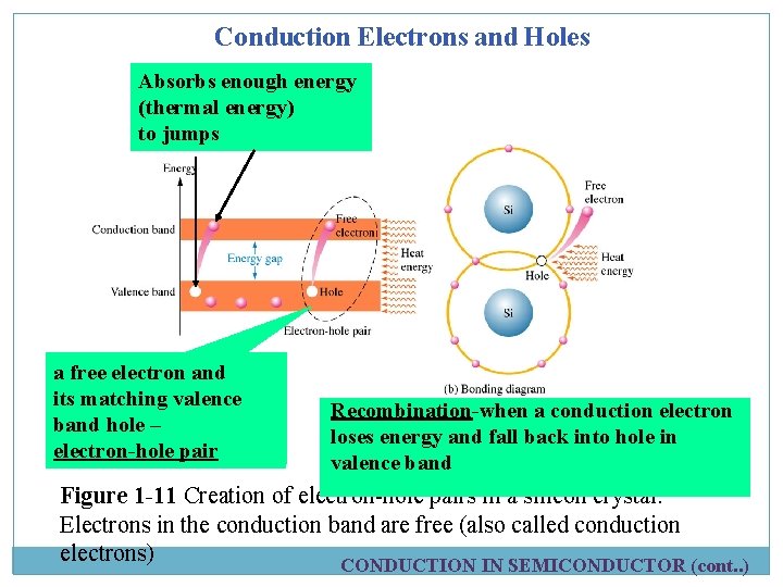
Conduction Electrons and Holes Absorbs enough energy (thermal energy) to jumps a free electron and its matching valence band hole – electron-hole pair Recombination-when a conduction electron loses energy and fall back into hole in valence band Figure 1 -11 Creation of electron-hole pairs in a silicon crystal. Electrons in the conduction band are free (also called conduction electrons) CONDUCTION IN SEMICONDUCTOR (cont. . )

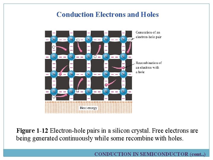
Conduction Electrons and Holes Figure 1 -12 Electron-hole pairs in a silicon crystal. Free electrons are being generated continuously while some recombine with holes. CONDUCTION IN SEMICONDUCTOR (cont. . )

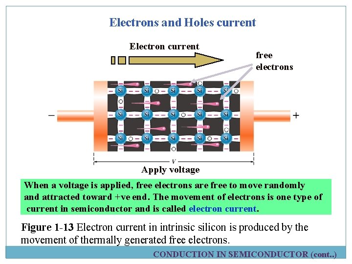
Electrons and Holes current Electron current free electrons Apply voltage When a voltage is applied, free electrons are free to move randomly and attracted toward +ve end. The movement of electrons is one type of current in semiconductor and is called electron current. Figure 1 -13 Electron current in intrinsic silicon is produced by the movement of thermally generated free electrons. CONDUCTION IN SEMICONDUCTOR (cont. . )

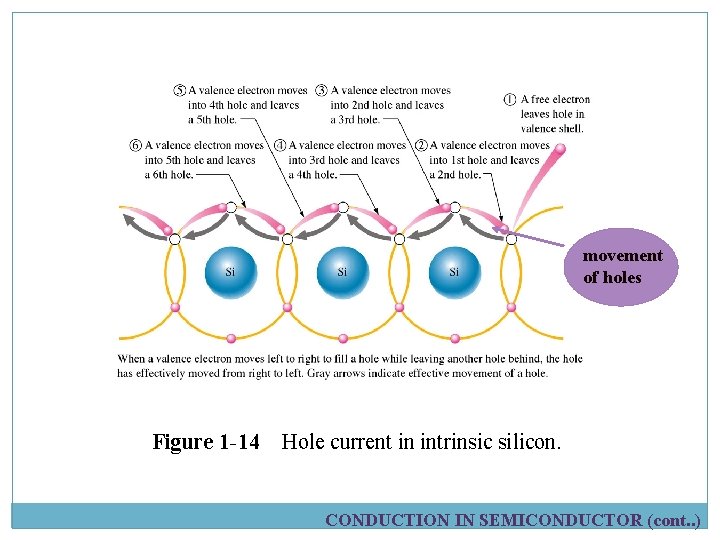
Electrons and Holes Current movement of holes Figure 1 -14 Hole current in intrinsic silicon. CONDUCTION IN SEMICONDUCTOR (cont. . )

Doping v The process of creating N and P type materials v By adding impurity atoms to intrinsic Si or Ge to improve the conductivity of the semiconductor v Two types of doping – trivalent (3 valence e-) & pentavalent (5 valence e-) p-type material – a semiconductor that has added trivalent impurities n-type material – a semiconductor that has added pentavalent impurities

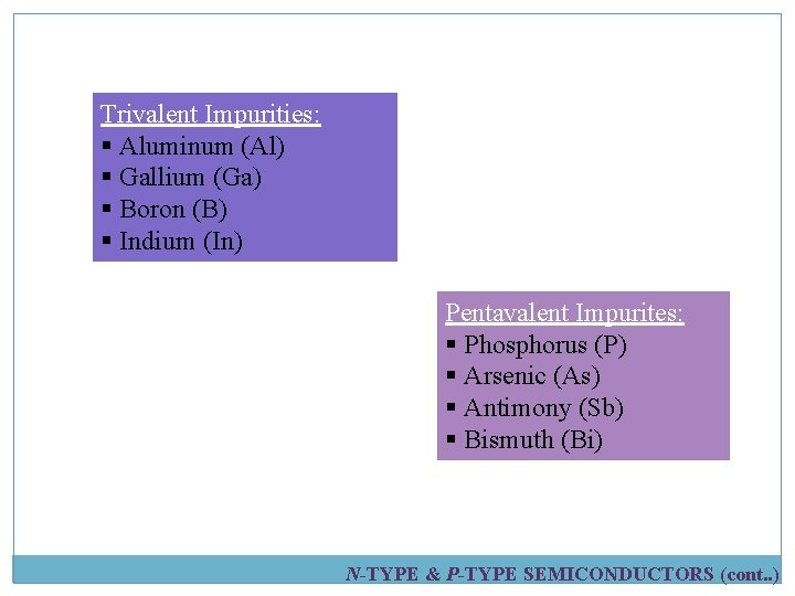
Trivalent Impurities: § Aluminum (Al) § Gallium (Ga) § Boron (B) § Indium (In) Pentavalent Impurites: § Phosphorus (P) § Arsenic (As) § Antimony (Sb) § Bismuth (Bi) N-TYPE & P-TYPE SEMICONDUCTORS (cont. . )

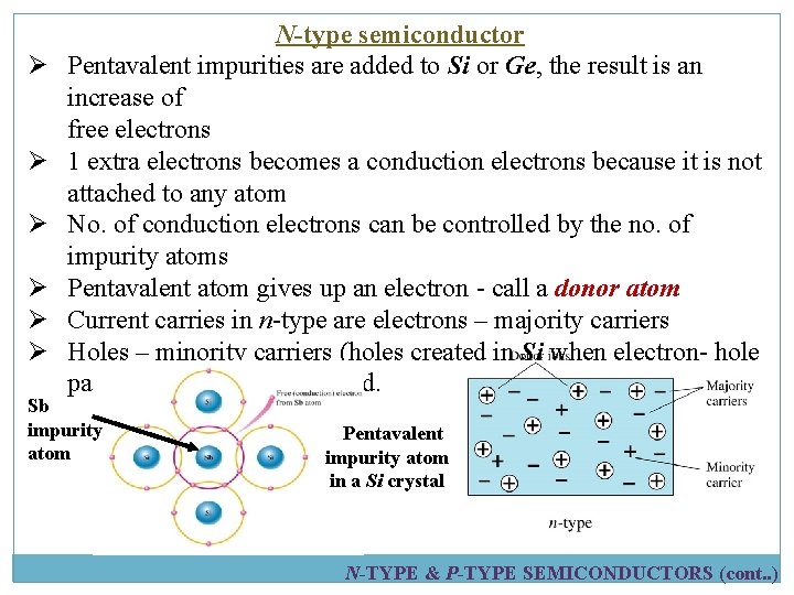
Ø Ø Ø N-type semiconductor Pentavalent impurities are added to Si or Ge, the result is an increase of free electrons 1 extra electrons becomes a conduction electrons because it is not attached to any atom No. of conduction electrons can be controlled by the no. of impurity atoms Pentavalent atom gives up an electron - call a donor atom Current carries in n-type are electrons – majority carriers Holes – minority carriers (holes created in Si when electron- hole pairs are thermally generated. Sb impurity atom Pentavalent impurity atom in a Si crystal N-TYPE & P-TYPE SEMICONDUCTORS (cont. . )

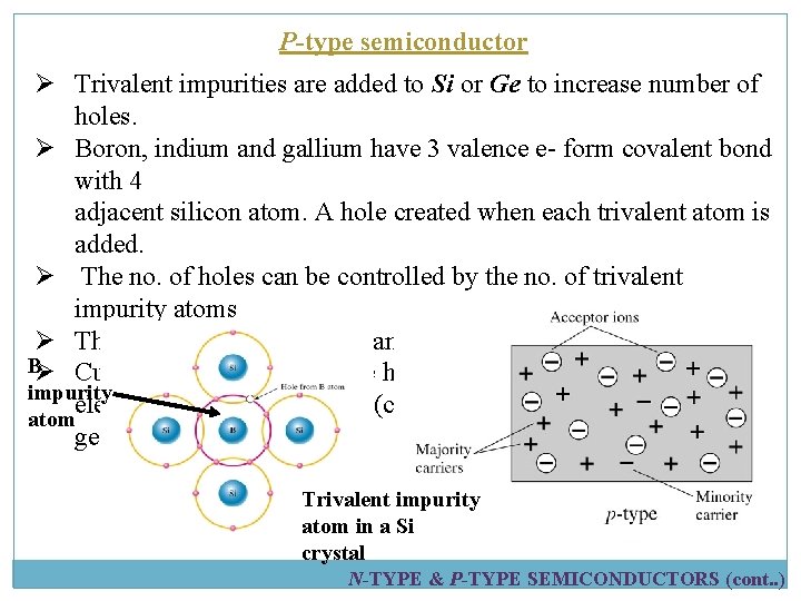
P-type semiconductor Ø Trivalent impurities are added to Si or Ge to increase number of holes. Ø Boron, indium and gallium have 3 valence e- form covalent bond with 4 adjacent silicon atom. A hole created when each trivalent atom is added. Ø The no. of holes can be controlled by the no. of trivalent impurity atoms Ø The trivalent atom can take an electron- acceptor atom BØ Current carries in p-type are holes – majority carries impurity electrons – minority carries (created during electron-holes pairs atom generation). Trivalent impurity atom in a Si crystal N-TYPE & P-TYPE SEMICONDUCTORS (cont. . )