Chapter 1 Semiconductor Diodes Semiconductor Materials commonly used
- Slides: 38

Chapter 1: Semiconductor Diodes

Semiconductor Materials commonly used in the development of semiconductor devices: • Silicon (Si) • Germanium (Ge) • Gallium Arsenide (Ga. As) Electronic Devices and Circuit Theory, 10/e Robert L. Boylestad and Louis Nashelsky 2 Copyright © 2009 by Pearson Education, Inc. Upper Saddle River, New Jersey 07458 • All rights reserved.

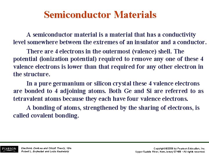
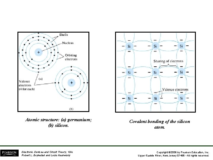
Semiconductor Materials A semiconductor material is a material that has a conductivity level somewhere between the extremes of an insulator and a conductor. There are 4 electrons in the outermost (valence) shell. The potential (ionization potential) required to remove any one of these 4 valence electrons is lower than that required for any other electron in the structure. In a pure germanium or silicon crystal these 4 valence electrons are bonded to 4 adjoining atoms. Both Ge and Si are referred to as tetravalent atoms because they each have four valence electrons. A bonding of atoms, strengthened by the sharing of electrons, is called covalent bonding. Electronic Devices and Circuit Theory, 10/e Robert L. Boylestad and Louis Nashelsky Copyright © 2009 by Pearson Education, Inc. Upper Saddle River, New Jersey 07458 • All rights reserved.

Atomic structure: (a) germanium; (b) silicon. Electronic Devices and Circuit Theory, 10/e Robert L. Boylestad and Louis Nashelsky Covalent bonding of the silicon atom. Copyright © 2009 by Pearson Education, Inc. Upper Saddle River, New Jersey 07458 • All rights reserved.

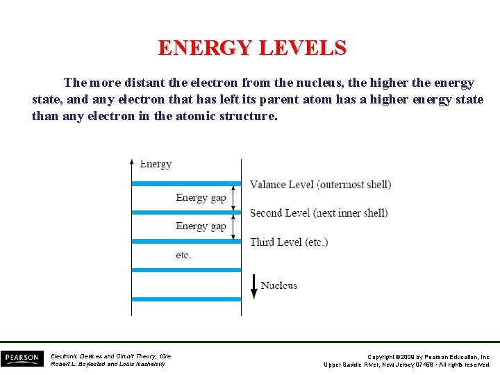
ENERGY LEVELS The more distant the electron from the nucleus, the higher the energy state, and any electron that has left its parent atom has a higher energy state than any electron in the atomic structure. Electronic Devices and Circuit Theory, 10/e Robert L. Boylestad and Louis Nashelsky Copyright © 2009 by Pearson Education, Inc. Upper Saddle River, New Jersey 07458 • All rights reserved.

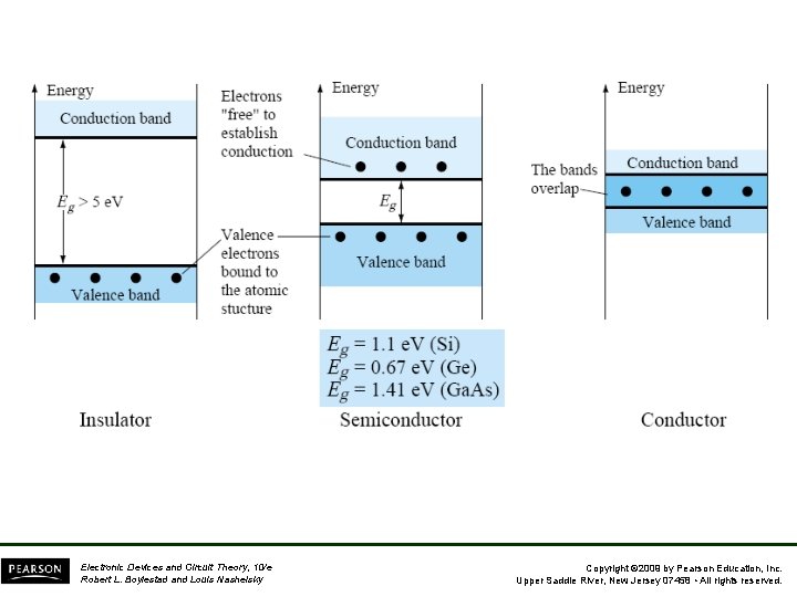
Electronic Devices and Circuit Theory, 10/e Robert L. Boylestad and Louis Nashelsky Copyright © 2009 by Pearson Education, Inc. Upper Saddle River, New Jersey 07458 • All rights reserved.

EXTRINSIC MATERIALS n- AND p-TYPE A semiconductor material that has been subjected to the doping process is called an extrinsic material. There are two extrinsic materials of semiconductor device fabrication: n-type and p-type. Electronic Devices and Circuit Theory, 10/e Robert L. Boylestad and Louis Nashelsky Copyright © 2009 by Pearson Education, Inc. Upper Saddle River, New Jersey 07458 • All rights reserved.

Doping The electrical characteristics of silicon and germanium are improved by adding materials in a process called doping. There are just two types of doped semiconductor materials: n-type p-type • n-type materials contain an excess of conduction band electrons. • p-type materials contain an excess of valence band holes. Electronic Devices and Circuit Theory, 10/e Robert L. Boylestad and Louis Nashelsky 8 Copyright © 2009 by Pearson Education, Inc. Upper Saddle River, New Jersey 07458 • All rights reserved.

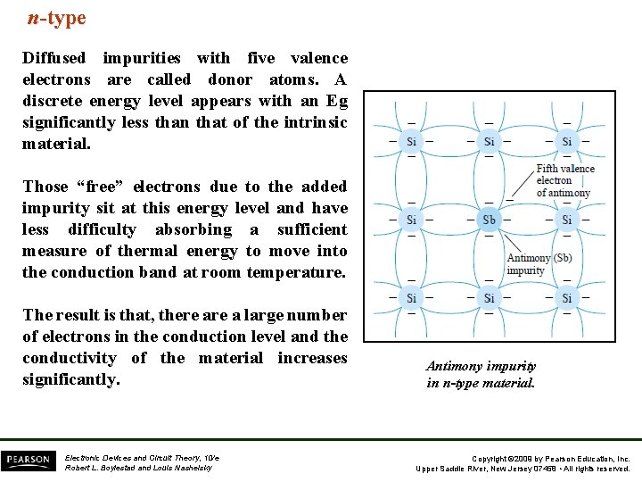
n-type Diffused impurities with five valence electrons are called donor atoms. A discrete energy level appears with an Eg significantly less than that of the intrinsic material. Those “free” electrons due to the added impurity sit at this energy level and have less difficulty absorbing a sufficient measure of thermal energy to move into the conduction band at room temperature. The result is that, there a large number of electrons in the conduction level and the conductivity of the material increases significantly. Electronic Devices and Circuit Theory, 10/e Robert L. Boylestad and Louis Nashelsky Antimony impurity in n-type material. Copyright © 2009 by Pearson Education, Inc. Upper Saddle River, New Jersey 07458 • All rights reserved.

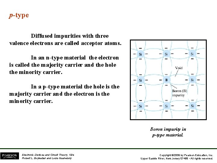
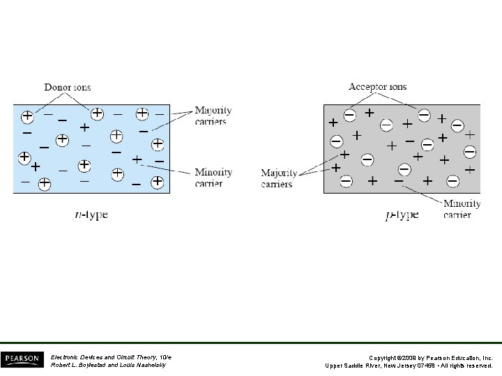
p-type Diffused impurities with three valence electrons are called acceptor atoms. In an n-type material the electron is called the majority carrier and the hole the minority carrier. In a p-type material the hole is the majority carrier and the electron is the minority carrier. Boron impurity in p-type material. Electronic Devices and Circuit Theory, 10/e Robert L. Boylestad and Louis Nashelsky Copyright © 2009 by Pearson Education, Inc. Upper Saddle River, New Jersey 07458 • All rights reserved.

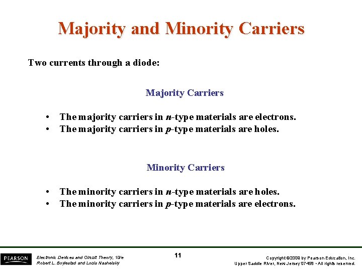
Majority and Minority Carriers Two currents through a diode: Majority Carriers • The majority carriers in n-type materials are electrons. • The majority carriers in p-type materials are holes. Minority Carriers • The minority carriers in n-type materials are holes. • The minority carriers in p-type materials are electrons. Electronic Devices and Circuit Theory, 10/e Robert L. Boylestad and Louis Nashelsky 11 Copyright © 2009 by Pearson Education, Inc. Upper Saddle River, New Jersey 07458 • All rights reserved.

Electronic Devices and Circuit Theory, 10/e Robert L. Boylestad and Louis Nashelsky Copyright © 2009 by Pearson Education, Inc. Upper Saddle River, New Jersey 07458 • All rights reserved.

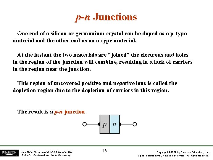
p-n Junctions One end of a silicon or germanium crystal can be doped as a p-type material and the other end as an n-type material. At the instant the two materials are “joined” the electrons and holes in the region of the junction will combine, resulting in a lack of carriers in the region near the junction. This region of uncovered positive and negative ions is called the depletion region due to the depletion of carriers in this region. The result is a p-n junction Electronic Devices and Circuit Theory, 10/e Robert L. Boylestad and Louis Nashelsky 13 Copyright © 2009 by Pearson Education, Inc. Upper Saddle River, New Jersey 07458 • All rights reserved.

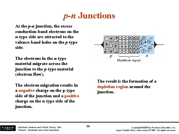
p-n Junctions At the p-n junction, the excess conduction-band electrons on the n-type side are attracted to the valence-band holes on the p-type side. The electrons in the n-type material migrate across the junction to the p-type material (electron flow). The result is the formation of a depletion region around the junction. The electron migration results in a negative charge on the p-type side of the junction and a positive charge on the n-type side of the junction. Electronic Devices and Circuit Theory, 10/e Robert L. Boylestad and Louis Nashelsky 14 Copyright © 2009 by Pearson Education, Inc. Upper Saddle River, New Jersey 07458 • All rights reserved.

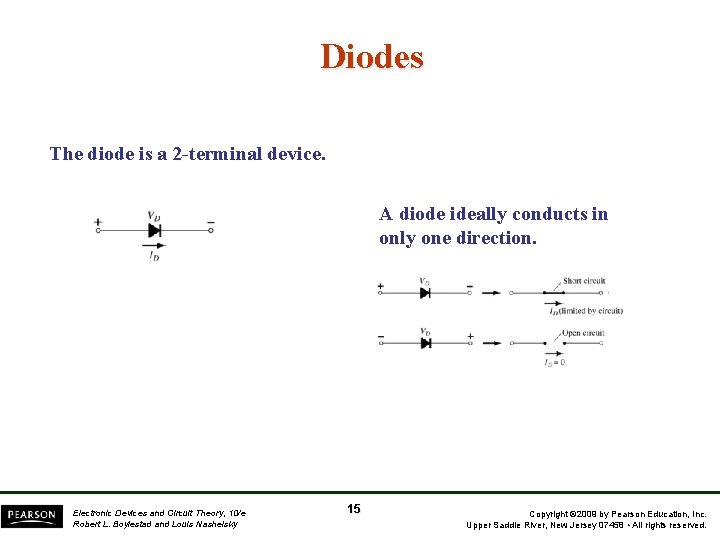
Diodes The diode is a 2 -terminal device. A diode ideally conducts in only one direction. Electronic Devices and Circuit Theory, 10/e Robert L. Boylestad and Louis Nashelsky 15 Copyright © 2009 by Pearson Education, Inc. Upper Saddle River, New Jersey 07458 • All rights reserved.

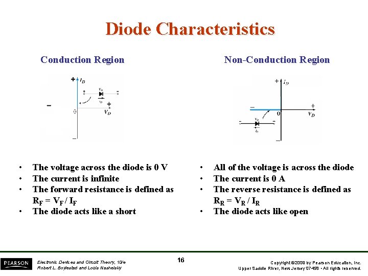
Diode Characteristics Conduction Region • • Non-Conduction Region • • • The voltage across the diode is 0 V The current is infinite The forward resistance is defined as RF = V F / I F The diode acts like a short Electronic Devices and Circuit Theory, 10/e Robert L. Boylestad and Louis Nashelsky • 16 All of the voltage is across the diode The current is 0 A The reverse resistance is defined as RR = V R / I R The diode acts like open Copyright © 2009 by Pearson Education, Inc. Upper Saddle River, New Jersey 07458 • All rights reserved.

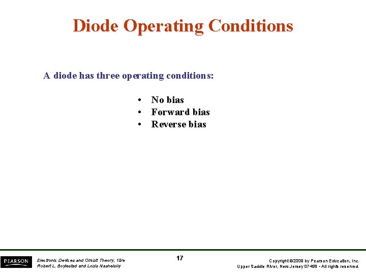
Diode Operating Conditions A diode has three operating conditions: • No bias • Forward bias • Reverse bias Electronic Devices and Circuit Theory, 10/e Robert L. Boylestad and Louis Nashelsky 17 Copyright © 2009 by Pearson Education, Inc. Upper Saddle River, New Jersey 07458 • All rights reserved.

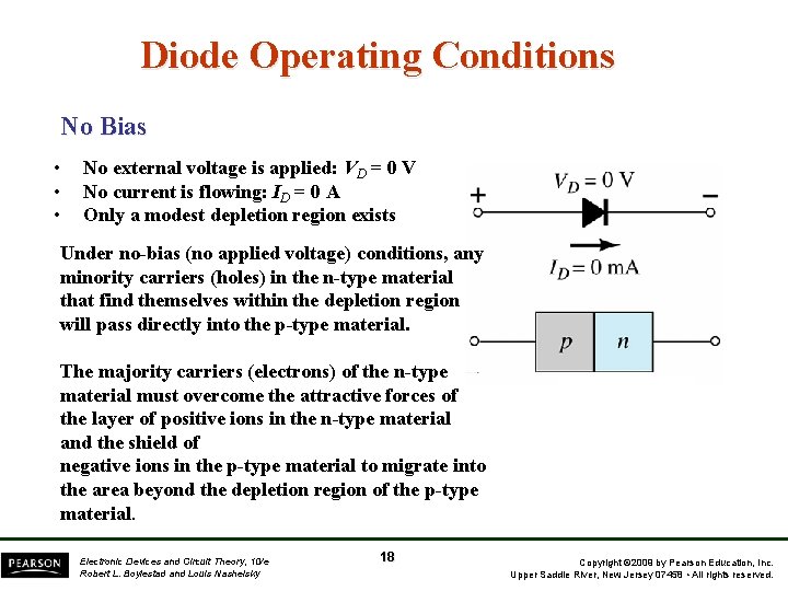
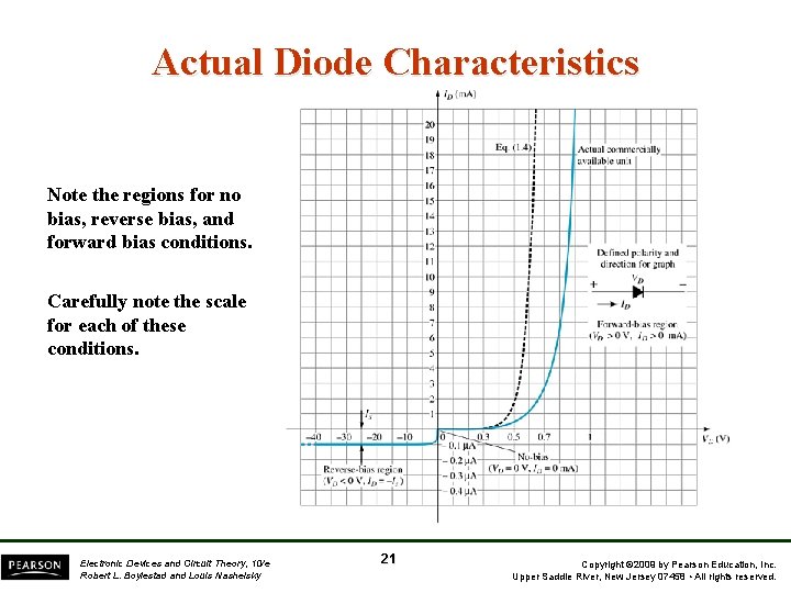
Diode Operating Conditions No Bias • • • No external voltage is applied: VD = 0 V No current is flowing: ID = 0 A Only a modest depletion region exists Under no-bias (no applied voltage) conditions, any minority carriers (holes) in the n-type material that find themselves within the depletion region will pass directly into the p-type material. The majority carriers (electrons) of the n-type material must overcome the attractive forces of the layer of positive ions in the n-type material and the shield of negative ions in the p-type material to migrate into the area beyond the depletion region of the p-type material. Electronic Devices and Circuit Theory, 10/e Robert L. Boylestad and Louis Nashelsky 18 Copyright © 2009 by Pearson Education, Inc. Upper Saddle River, New Jersey 07458 • All rights reserved.

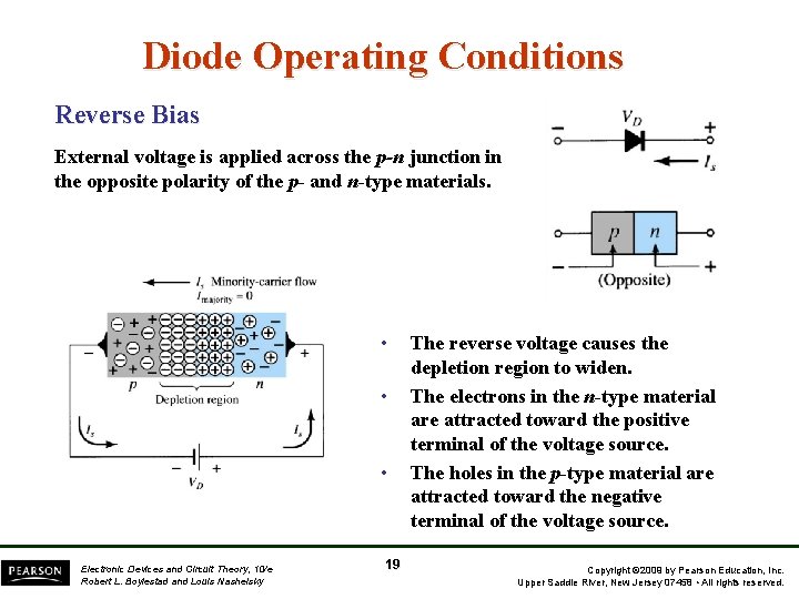
Diode Operating Conditions Reverse Bias External voltage is applied across the p-n junction in the opposite polarity of the p- and n-type materials. • • • Electronic Devices and Circuit Theory, 10/e Robert L. Boylestad and Louis Nashelsky 19 The reverse voltage causes the depletion region to widen. The electrons in the n-type material are attracted toward the positive terminal of the voltage source. The holes in the p-type material are attracted toward the negative terminal of the voltage source. Copyright © 2009 by Pearson Education, Inc. Upper Saddle River, New Jersey 07458 • All rights reserved.

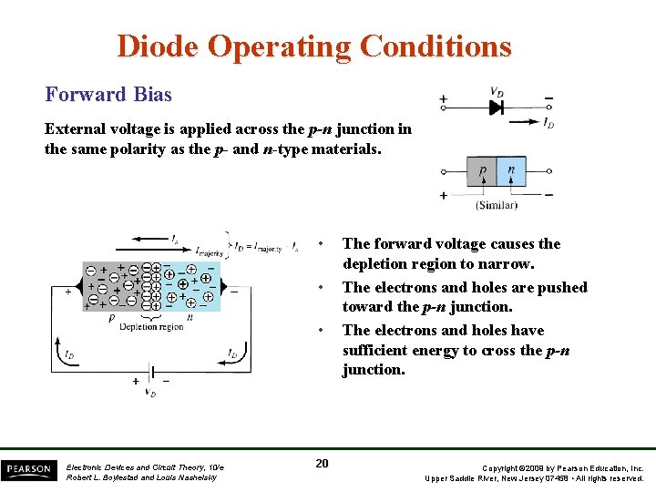
Diode Operating Conditions Forward Bias External voltage is applied across the p-n junction in the same polarity as the p- and n-type materials. • • • Electronic Devices and Circuit Theory, 10/e Robert L. Boylestad and Louis Nashelsky 20 The forward voltage causes the depletion region to narrow. The electrons and holes are pushed toward the p-n junction. The electrons and holes have sufficient energy to cross the p-n junction. Copyright © 2009 by Pearson Education, Inc. Upper Saddle River, New Jersey 07458 • All rights reserved.

Actual Diode Characteristics Note the regions for no bias, reverse bias, and forward bias conditions. Carefully note the scale for each of these conditions. Electronic Devices and Circuit Theory, 10/e Robert L. Boylestad and Louis Nashelsky 21 Copyright © 2009 by Pearson Education, Inc. Upper Saddle River, New Jersey 07458 • All rights reserved.

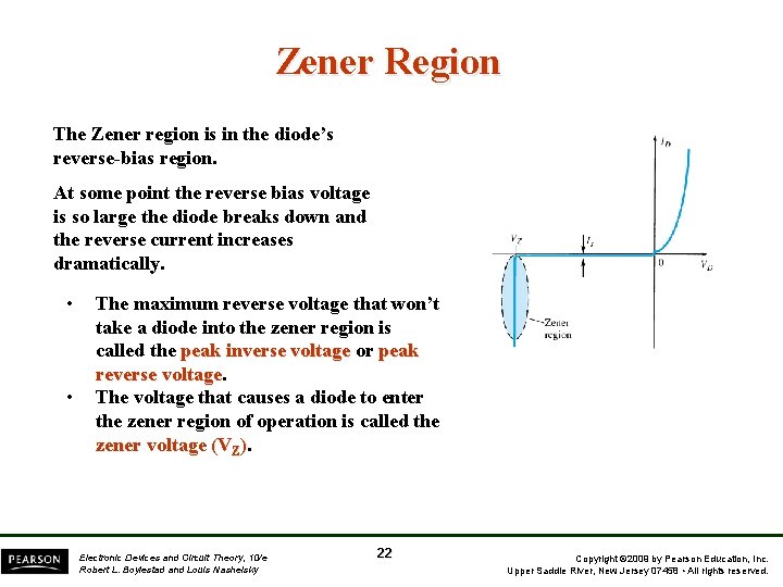
Zener Region The Zener region is in the diode’s reverse-bias region. At some point the reverse bias voltage is so large the diode breaks down and the reverse current increases dramatically. • • The maximum reverse voltage that won’t take a diode into the zener region is called the peak inverse voltage or peak reverse voltage The voltage that causes a diode to enter the zener region of operation is called the zener voltage (VZ). Electronic Devices and Circuit Theory, 10/e Robert L. Boylestad and Louis Nashelsky 22 Copyright © 2009 by Pearson Education, Inc. Upper Saddle River, New Jersey 07458 • All rights reserved.

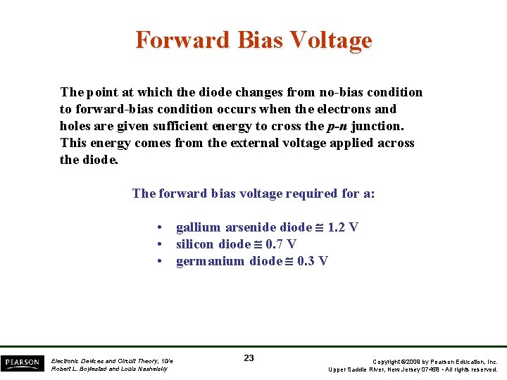
Forward Bias Voltage The point at which the diode changes from no-bias condition to forward-bias condition occurs when the electrons and holes are given sufficient energy to cross the p-n junction. This energy comes from the external voltage applied across the diode. The forward bias voltage required for a: • gallium arsenide diode 1. 2 V • silicon diode 0. 7 V • germanium diode 0. 3 V Electronic Devices and Circuit Theory, 10/e Robert L. Boylestad and Louis Nashelsky 23 Copyright © 2009 by Pearson Education, Inc. Upper Saddle River, New Jersey 07458 • All rights reserved.

Temperature Effects As temperature increases it adds energy to the diode. • It reduces the required forward bias voltage forwardbias conduction. • It increases the amount of reverse current in the reversebias condition. • It increases maximum reverse bias avalanche voltage. Germanium diodes are more sensitive to temperature variations than silicon or gallium arsenide diodes. Electronic Devices and Circuit Theory, 10/e Robert L. Boylestad and Louis Nashelsky 24 Copyright © 2009 by Pearson Education, Inc. Upper Saddle River, New Jersey 07458 • All rights reserved.

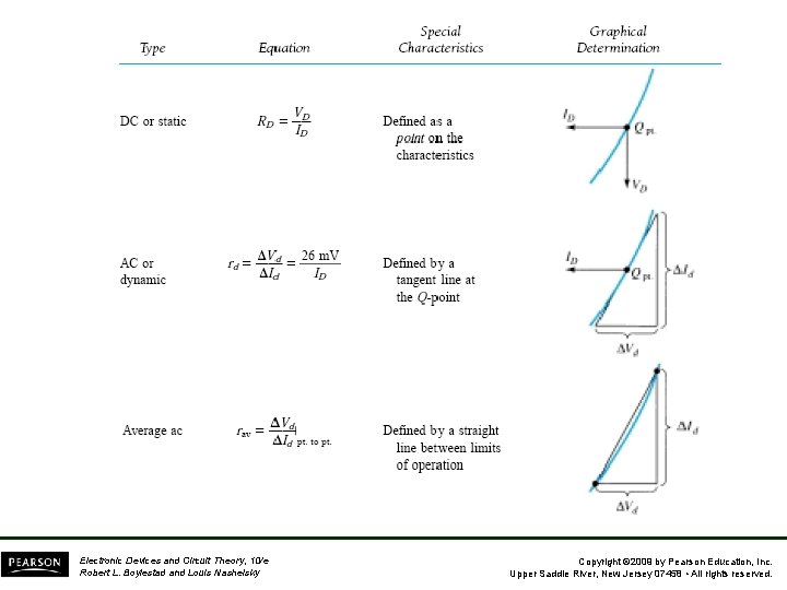
Resistance Levels Semiconductors react differently to DC and AC currents. There are three types of resistance: • DC (static) resistance • AC (dynamic) resistance • Average AC resistance Electronic Devices and Circuit Theory, 10/e Robert L. Boylestad and Louis Nashelsky 25 Copyright © 2009 by Pearson Education, Inc. Upper Saddle River, New Jersey 07458 • All rights reserved.

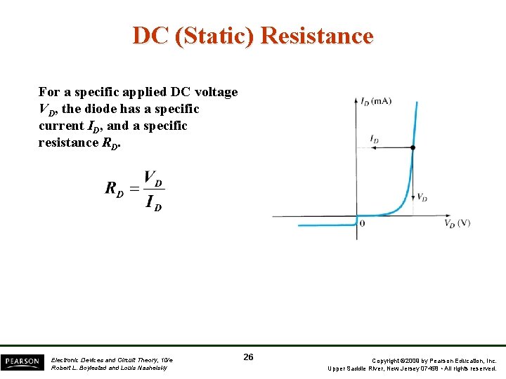
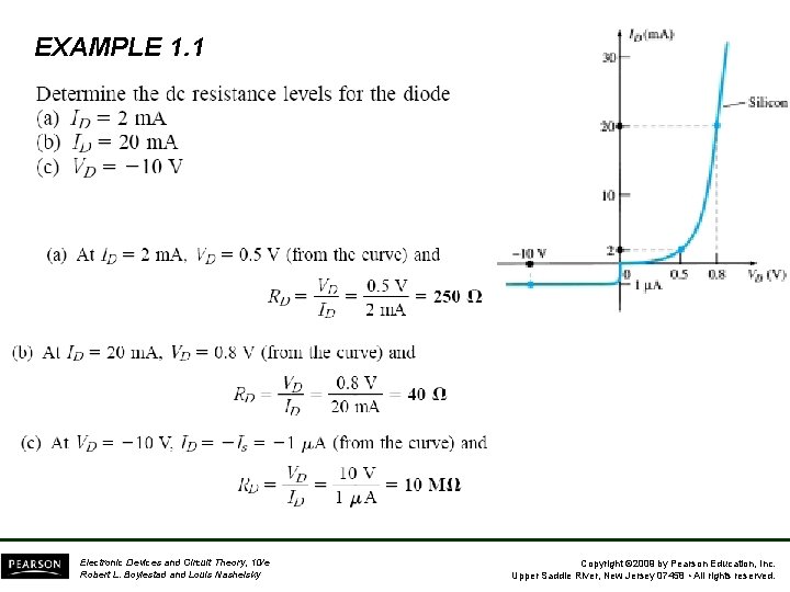
DC (Static) Resistance For a specific applied DC voltage VD, the diode has a specific current ID, and a specific resistance RD. Electronic Devices and Circuit Theory, 10/e Robert L. Boylestad and Louis Nashelsky 26 Copyright © 2009 by Pearson Education, Inc. Upper Saddle River, New Jersey 07458 • All rights reserved.

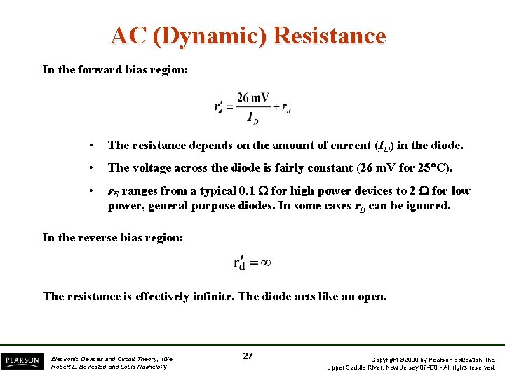
AC (Dynamic) Resistance In the forward bias region: • The resistance depends on the amount of current (ID) in the diode. • The voltage across the diode is fairly constant (26 m. V for 25 C). • r. B ranges from a typical 0. 1 for high power devices to 2 for low power, general purpose diodes. In some cases r. B can be ignored. In the reverse bias region: The resistance is effectively infinite. The diode acts like an open. Electronic Devices and Circuit Theory, 10/e Robert L. Boylestad and Louis Nashelsky 27 Copyright © 2009 by Pearson Education, Inc. Upper Saddle River, New Jersey 07458 • All rights reserved.

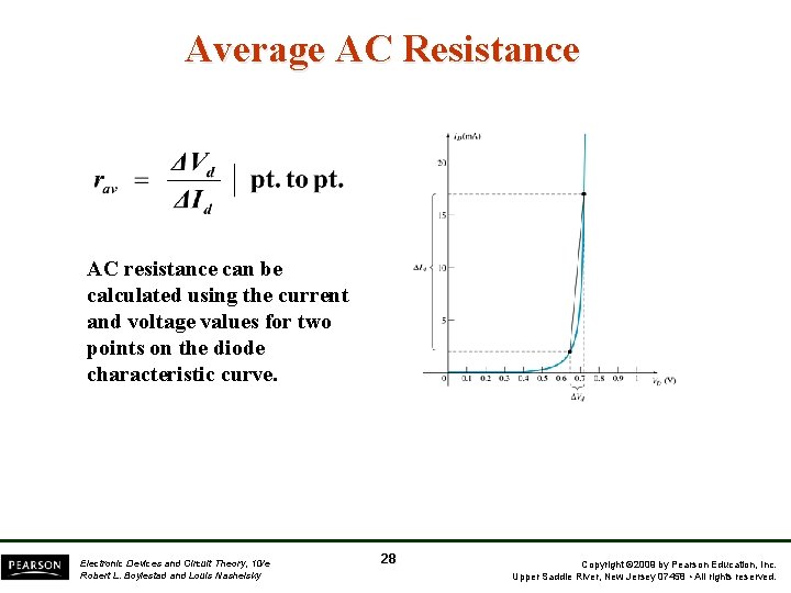
Average AC Resistance AC resistance can be calculated using the current and voltage values for two points on the diode characteristic curve. Electronic Devices and Circuit Theory, 10/e Robert L. Boylestad and Louis Nashelsky 28 Copyright © 2009 by Pearson Education, Inc. Upper Saddle River, New Jersey 07458 • All rights reserved.

Electronic Devices and Circuit Theory, 10/e Robert L. Boylestad and Louis Nashelsky Copyright © 2009 by Pearson Education, Inc. Upper Saddle River, New Jersey 07458 • All rights reserved.

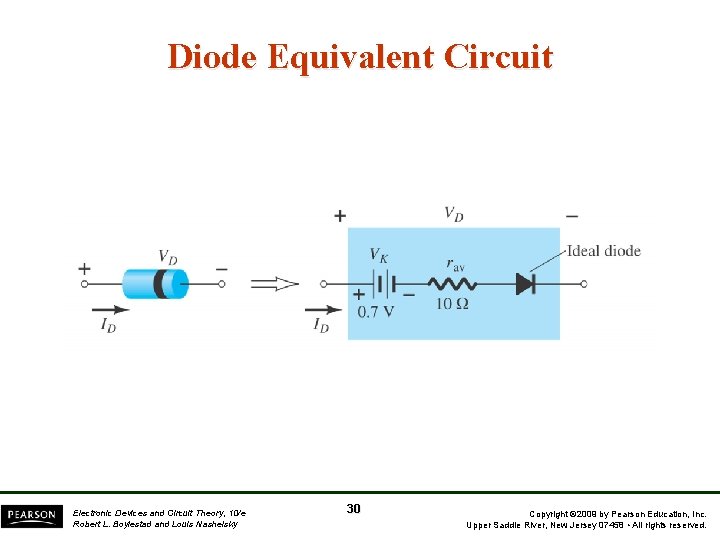
Diode Equivalent Circuit Electronic Devices and Circuit Theory, 10/e Robert L. Boylestad and Louis Nashelsky 30 Copyright © 2009 by Pearson Education, Inc. Upper Saddle River, New Jersey 07458 • All rights reserved.

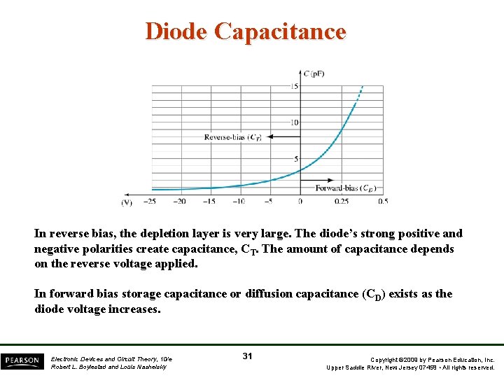
Diode Capacitance In reverse bias, the depletion layer is very large. The diode’s strong positive and negative polarities create capacitance, CT. The amount of capacitance depends on the reverse voltage applied. In forward bias storage capacitance or diffusion capacitance (CD) exists as the diode voltage increases. Electronic Devices and Circuit Theory, 10/e Robert L. Boylestad and Louis Nashelsky 31 Copyright © 2009 by Pearson Education, Inc. Upper Saddle River, New Jersey 07458 • All rights reserved.

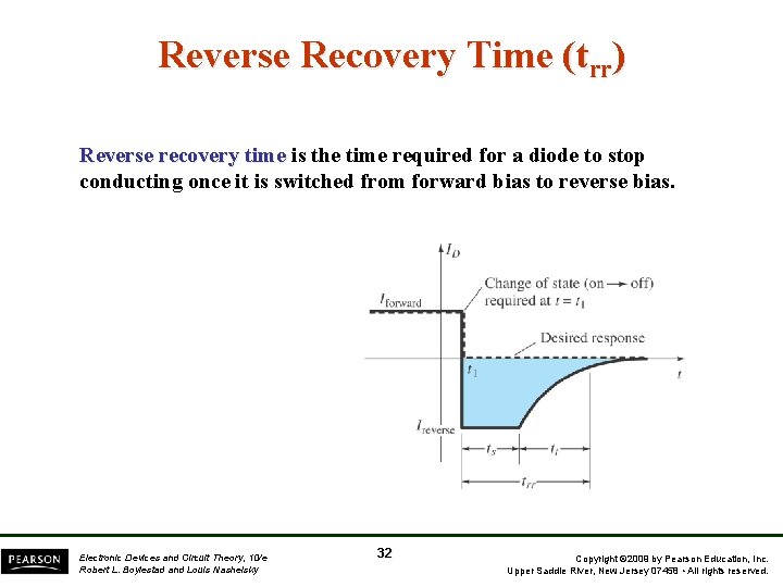
Reverse Recovery Time (trr) Reverse recovery time is the time required for a diode to stop conducting once it is switched from forward bias to reverse bias. Electronic Devices and Circuit Theory, 10/e Robert L. Boylestad and Louis Nashelsky 32 Copyright © 2009 by Pearson Education, Inc. Upper Saddle River, New Jersey 07458 • All rights reserved.

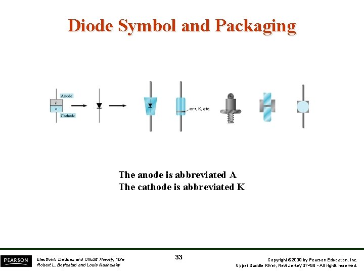
Diode Symbol and Packaging The anode is abbreviated A The cathode is abbreviated K Electronic Devices and Circuit Theory, 10/e Robert L. Boylestad and Louis Nashelsky 33 Copyright © 2009 by Pearson Education, Inc. Upper Saddle River, New Jersey 07458 • All rights reserved.

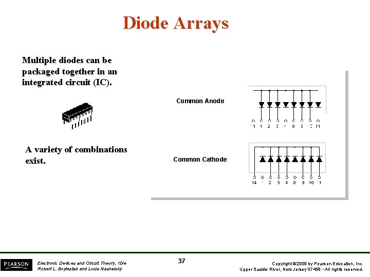
Other Types of Diodes Zener diode Light-emitting diode Diode arrays Electronic Devices and Circuit Theory, 10/e Robert L. Boylestad and Louis Nashelsky 34 Copyright © 2009 by Pearson Education, Inc. Upper Saddle River, New Jersey 07458 • All rights reserved.

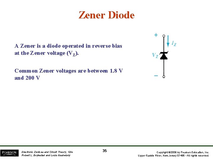
Zener Diode A Zener is a diode operated in reverse bias at the Zener voltage (VZ). Common Zener voltages are between 1. 8 V and 200 V Electronic Devices and Circuit Theory, 10/e Robert L. Boylestad and Louis Nashelsky 35 Copyright © 2009 by Pearson Education, Inc. Upper Saddle River, New Jersey 07458 • All rights reserved.

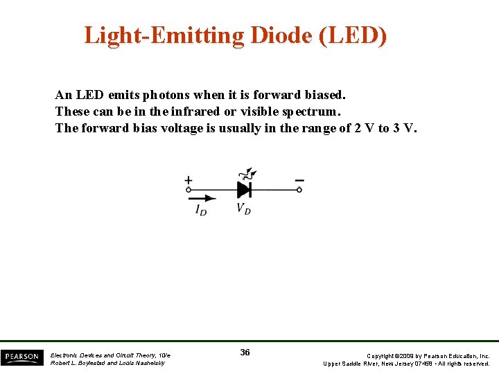
Light-Emitting Diode (LED) An LED emits photons when it is forward biased. These can be in the infrared or visible spectrum. The forward bias voltage is usually in the range of 2 V to 3 V. Electronic Devices and Circuit Theory, 10/e Robert L. Boylestad and Louis Nashelsky 36 Copyright © 2009 by Pearson Education, Inc. Upper Saddle River, New Jersey 07458 • All rights reserved.

Diode Arrays Multiple diodes can be packaged together in an integrated circuit (IC). Common Anode A variety of combinations exist. Electronic Devices and Circuit Theory, 10/e Robert L. Boylestad and Louis Nashelsky Common Cathode 37 Copyright © 2009 by Pearson Education, Inc. Upper Saddle River, New Jersey 07458 • All rights reserved.

EXAMPLE 1. 1 Electronic Devices and Circuit Theory, 10/e Robert L. Boylestad and Louis Nashelsky Copyright © 2009 by Pearson Education, Inc. Upper Saddle River, New Jersey 07458 • All rights reserved.