
Chapter 1 MICROPROCESSORS EVOLUTION INTRODUCTION TO 8085 212022






- Slides: 110
Chapter 1 MICROPROCESSORS- EVOLUTION & INTRODUCTION TO 8085 2/1/2022 Ravindra College of Engineering for Women
Introduction • Microprocessor is an electronic chip that functions as the central processing unit (CPU) of a computer • In other words, we can call microprocessor as the heart of any computer system. • Some may call the microprocessors as the brain of the computers. • The microprocessor based systems with limited resources are called as microcomputers. • Now-a-days microprocessors are found in almost all electronic machines and appliances in its different form 2/1/2022 Ravindra College of Engineering for Women
Introduction • Some common devices using microprocessors are computer printers, automobiles, washing machines, microwave ovens, mobile phones, fax machines, Xerox machines and advanced instruments like radar, satellites, flights etc. , • Any middle class house-hold will have about a dozens microprocessor in different forms inside various appliances. • The recent developments in electronic industry and the large scale integration of devices has led to rapid cost reduction and more application of microprocessors and its derivatives. 2/1/2022 Ravindra College of Engineering for Women
Introduction • Almost all microprocessors use the basic concept of “stored program execution”. • By this concept, programs or the instructions to be executed by the microprocessor are stored sequentially in memory locations. • The microprocessor or the processor in general will fetch the instructions one after the other and execute them it in its arithmetic and logic unit. 2/1/2022 Ravindra College of Engineering for Women
Introduction • A microprocessor can be programmed to do any task that can be written and programmed by the user. • So, in order to work with the microprocessor, it is necessary for the user to know about the internal resources and features of the microprocessor. • The programmers must also understand the instructions that a microprocessor can support. • Every microprocessor will have its own associated set of instructions that it supports and this list is given by all the microprocessor manufacturers 2/1/2022 Ravindra College of Engineering for Women
Introduction • The instruction set for microprocessors is given in two forms a) one in mnemonic which is comparatively easy to understand b) the other in binary machine code which the microprocessor really works upon and difficult to understand by us. • Programs are written using mnemonics called the assembly level language and then they are converted into binary machine level language. • This conversion can be done manually or using an application called assembler. 2/1/2022 Ravindra College of Engineering for Women
Introduction • In general, the programs are written by the user for a microprocessor to work with real world data. • These data are available in many forms and are from many sources. • To give this data to the microprocessor, the microprocessor based systems need some input interfacing circuits and some electronic processing circuits. • These circuits include data converters and ports 2/1/2022 Ravindra College of Engineering for Women
Introduction • After processing the real world data, the output from the microprocessor must be taken out to give to final end effect instrument or circuits. • This again needs interfacing circuits and ports. • So, a microprocessor based system will need a set of memory units, set of interfacing circuits for inputs and a set of interfacing circuits for outputs. 2/1/2022 Ravindra College of Engineering for Women
Introduction • All circuits put together along with microprocessor are called as microcomputer system. • The physical components of the microcomputer system are in general called as hardware. • The program which makes this hardware useful is called as software. 2/1/2022 Ravindra College of Engineering for Women
Basic terms • Chip a) A chip or an integrated circuit is a small, thin piece of silicon with the required circuit and transistors etched on it to perform a particular function. b) Simpler processors might consist of a few thousand transistors etched onto a silicon base just a few millimeters square. 2/1/2022 Ravindra College of Engineering for Women
Basic terms • Bit a) A bit means a single binary digit. b) Also, the bit is the fundamental storage unit of computer memory. In binary, bit can have only two values, 0 or 1, whereas a decimal digit can have 10 values, represented by symbols 0 through 9. • Bit Size The bit size of a microprocessor refers to the number of bits that can be processed simultaneously by the basic arithmetic circuits of the microprocessor. 2/1/2022 Ravindra College of Engineering for Women
Basic terms • Word A number of bits grouped together for processing is called as word. In microprocessors, the word in general refers to the basic data size or bit size that can processed by the ALU of the processor. 16 -bit binary number is called a word in a 16 -bit processor. • Memory word The number of bits that can be stored in a register of memory element is called a memory word. Mostly all memory units use 8 -bits as their memory word. 2/1/2022 Ravindra College of Engineering for Women
Basic terms • Byte An 8 -bit word is referred to as a byte • Nibble A 4 -bit word is referred to as a nibble • Kilobyte A collection of 1024 bytes is called a kilobyte (210 bytes) • Megabyte A collection of 1024 Kbytes is called a megabyte (220 bytes) 2/1/2022 Ravindra College of Engineering for Women
Basic terms • RAM or R/W memory a) Random Access Memory or Read/ Write memory is the type of semiconductor memory in which a particular memory location can be erased and written with a new data at any time. b) These memory units are volatile, which means that the content of the memory is erased when the power to the chip is disrupted. c) The access of the individual memory location can be done randomly. In microprocessors, the RAM is used to store data. 2/1/2022 Ravindra College of Engineering for Women
Basic terms • DRAM a) Dynamic Random Access Memory is a semiconductor memory in which the stored contents need to be refreshed repeatedly at about thousands of times per second. b) Without refreshing, the stored data will be lost. c) These memory chips are preferred in a computer system because it is economical although slower. 2/1/2022 Ravindra College of Engineering for Women
Basic terms • SRAM – Static Random Access Memory chips keep the data stored in it as long as power is available. There is no need for refreshing. In terms of speed, SRAM is faster. • ROM – Read Only Memory are memory devices whose contents are retained even after removing the power supply. 2/1/2022 Ravindra College of Engineering for Women
Basic terms • Arithmetic and Logic Unit (ALU) a) ALU is a digital circuit present in the microprocessor to do performs arithmetic and logic operations on digital data. b) The typical operations performed by the ALU are addition, subtraction, Logical AND, logical OR and comparison of binary data. c) Generally, the functions of the ALU of a microprocessor will decide the functionality that can be performed by the processor. 2/1/2022 Ravindra College of Engineering for Women
Basic terms • Microcontroller is a chip that includes microprocessor, memory and I/O signal ports. Microcontrollers can be called as single chip microcomputers. • Microcomputer The system formed by interfacing microprocessor with memory, and I/O devices to work with the required program is called microcomputer. • Bus The bus in a microprocessor system refers to a group of wires or signals having a common functionality 2/1/2022 Ravindra College of Engineering for Women
Basic terms • System Bus The System bus is a group of signals used for communication between the microprocessor and peripherals. • Firmware Software written for a microprocessor application without provision for changes. These are stored into permanent storage or ROM of the computer system. 2/1/2022 Ravindra College of Engineering for Women
Basic terms • Input device The devices that are used for giving data to the microcomputer system are called as input devices. Usually keyboard and mouse are the input devices through which data and instructions are given to computer. • Output device The devices that are used for getting data out from the microprocessor or microcomputer system are called as output devices. A display screen, printer and displays are the common output devices. 2/1/2022 Ravindra College of Engineering for Women
Basic terms • Floppy disk A removable type magnetic disk used for storing programs and data from and to the computer. • Disk drive The hardware component that is used to read or write to data to devices such as a floppy disk. • Computer architecture The design and internal configuration and accesses in a digital computer 2/1/2022 Ravindra College of Engineering for Women
Basic terms • Von-Neumann Architecture The architecture in which the same memory is used for storing the program as well as data. • Harvard Architecture The architecture in which the program and data are stored in two separate memory units. • CISC Processor “Complex Instruction Set Computer”, is a processor architecture that supports many number of machine language instructions. 2/1/2022 Ravindra College of Engineering for Women
Basic terms • RISC processor a) “Reduced Instruction Set Architecture”, is a processor architecture that supports limited or small number of machine language instructions. b) RISC processors are expected to execute the programs faster than CISC processors. • High level Language a) A computer programming language in which programs are written without the knowledge of the processor in which the program will be executed. b) BASIC, FORTRAN, C, PASCAL and JAVA are the examples of high level languages. 2/1/2022 Ravindra College of Engineering for Women
Basic terms • Assembly Language a) A programming language written using the mnemonics or the instruction set of a particular microprocessor. b) Assembly language programming is microprocessor specific. c) It cannot be easily understood like a high level language program. d) But these are easier than machine language program. 2/1/2022 Ravindra College of Engineering for Women
Basic terms • Machine Language a) The binary code programs that are specific to the processor and can be directly executed by the processor. b) The machine language is the lowest level program and cannot be easily understood. • Assembler A computer application program that converts the assembly language program into machine level language program. 2/1/2022 Ravindra College of Engineering for Women
Basic terms • Compiler A computer program that converts the high level language program into machine level language program. • Interpreter a) A computer program that reads the high level or assembly level program one line at time and converts that into machine level program. b) Compiler and assembler can function only on the entire program in a file. 2/1/2022 Ravindra College of Engineering for Women
Basic terms • Algorithm a) A sequence of operations or instructions that defines how to solve a problem using a computer or microcomputer. b) An algorithm must be definite and follow a clear instruction flow without any ambiguity and must have a definite starting and end point. 2/1/2022 Ravindra College of Engineering for Women
Basic terms • BIOS a) Basic Input/ Output System is a set of program that handles the input and output functions and interacts with the hardware directly. b) A new hardware installed must be provided with the corresponding BIOS routines. 2/1/2022 Ravindra College of Engineering for Women
Basic terms • Clock a) The circuit in the computer that generates the sequence of evenly spaced pulses to synchronize the activities of the processor and its peripherals. b) The clock speed determines the speed of the operation of the computer. c) The computer with a high frequency clock works faster. Normally the clock frequency is in the range of Mega Hertz, MHz or Giga Hertz, GHz. 2/1/2022 Ravindra College of Engineering for Women
Basic terms • MIPS "Millions Instructions per Second" is a measure of the speed at which the instructions are executed in a processor. • Tri-state logic a) Three Logic Levels used are High (1), Low (0), High impedance state (Z). b) The logic high state of digital circuit can source current and a logic low can sink current in a computer system. c)But high impedance state neither sources current and nor sinks current and so the other devices connected to it are not affected. 2/1/2022 Ravindra College of Engineering for Women
Basic terms • Operating System a) The program that controls the entire computer and its resources and enables users to access the computer and its resources. b) Under the control of the operating system, the computer recognizes and obeys commands typed by the user. c) In addition, the operating system provides built-in routines that allow the user’s program to perform inputoutput operations without specifying the exact hardware configuration of the computer. d) In low level microprocessor based systems, the program that controls the hardware is called as monitor routines or monitor software. Ravindra College of Engineering for Women 2/1/2022
Types of Processors • Two types of processors are manufactured a) the microprocessor b) the microcontroller • The general purpose microprocessors give the computers all the necessary computing power. • These microprocessors need additional circuitry elements such as memory devices, I/O ports to connect the input and output devices. • All microprocessor based systems need two types of memories – RAM and ROM. 2/1/2022 Ravindra College of Engineering for Women
Microcontrollers • The microcontrollers are the microprocessors designed especially for control applications. • Microcontrollers contain memory units and I/O ports inside a chip in addition to the CPU part. • Microcontrollers are otherwise called as embedded controllers are generally used to control and operate smart machines. • Some of the machines using microcontrollers are microwave ovens, washing machines, sewing machines, automobile ignition systems, computer printers and fax machines etc. 2/1/2022 Ravindra College of Engineering for Women
Microcontrollers • Out of 100 processor chips manufactured, 99 are embedded processors and remaining 1 processor alone goes into general computers. • Lots of semiconductor companies are in the market of microcontrollers and any application development engineer is flooded with the variety of microcontrollers as the choice. 2/1/2022 Ravindra College of Engineering for Women
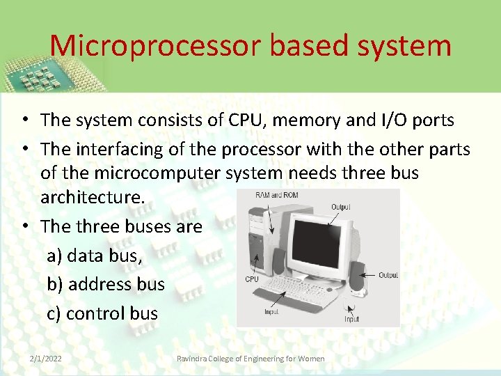
Microprocessor based system • The system consists of CPU, memory and I/O ports • The interfacing of the processor with the other parts of the microcomputer system needs three bus architecture. • The three buses are a) data bus, b) address bus c) control bus 2/1/2022 Ravindra College of Engineering for Women
Microprocessor based system • Each memory location or I/O port is identified by a specific address similar to the postal address. • Here, in microprocessor systems, the addresses are all in binary and in general written in hexadecimal number format. • The address is a unique pattern used to identify a location in memory or I/O port. • The address bus consists of many lines that can have the digital data sent by the processor. 2/1/2022 Ravindra College of Engineering for Women
Microprocessor based system • An address bus of 8 bits 28 different memory locations. • Similarly, the 16 -bit address bus can address 216 different addresses. Its address ranges from 0000 H to FFFFH. • The higher the number of lines of address bus is, the more the locations the processor is able to manage. 2/1/2022 Ravindra College of Engineering for Women
Microprocessor based system • A control bus is needed for proper data transfer between the processor and other peripherals. • The control bus basically consists of signals like selecting the proper memory or I/O device from the address; signal to indicate the direction of data transfer; and the signal to synchronize data transfer between slow devices. 2/1/2022 Ravindra College of Engineering for Women
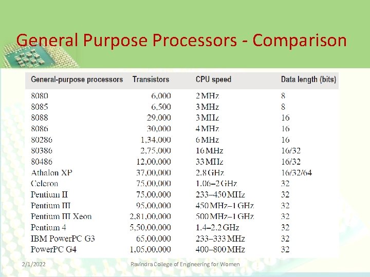
Origin of Microprocessor • The breakthrough in transistor technology led to the introduction of minicomputers of the 1960 s and the personal computer revolution of the 1970 s. • Intel was the first MPU producer and has been holding a large share in the world market of this product. • Microprocessors evolution is categorized into five generations – first, second, third, fourth, and fifth generations. 2/1/2022 Ravindra College of Engineering for Women
First Generation (1971 -73) • The microprocessors that were introduced in 1971 to 1972 were referred to as the first generation systems. • Intel Corporation introduced 4 -bit 4004 at 108 k. Hz, the first microprocessor in 1971, co-developed by Busicom, a Japanese manufacturer of calculators. • In 1972, Intel made the 8 -bit 8008 and 8080 microprocessors. 2/1/2022 Ravindra College of Engineering for Women
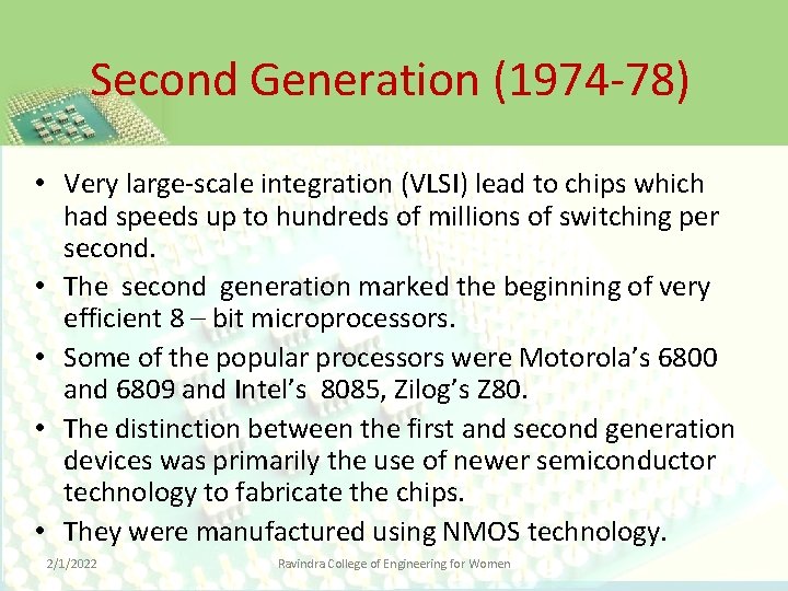
Second Generation (1974 -78) • Very large-scale integration (VLSI) lead to chips which had speeds up to hundreds of millions of switching per second. • The second generation marked the beginning of very efficient 8 – bit microprocessors. • Some of the popular processors were Motorola’s 6800 and 6809 and Intel’s 8085, Zilog’s Z 80. • The distinction between the first and second generation devices was primarily the use of newer semiconductor technology to fabricate the chips. • They were manufactured using NMOS technology. 2/1/2022 Ravindra College of Engineering for Women
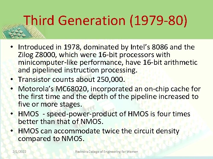
Third Generation (1979 -80) • Introduced in 1978, dominated by Intel’s 8086 and the Zilog Z 8000, which were 16 -bit processors with minicomputer-like performance, have 16 -bit arithmetic and pipelined instruction processing. • Transistor counts about 250, 000. • Motorola’s MC 68020, incorporated an on-chip cache for the first time and the depth of the pipeline increased to five or more stages. • HMOS - speed-power-product of HMOS is four times better than that of NMOS. • HMOS can accommodate twice the circuit density compared to NMOS. 2/1/2022 Ravindra College of Engineering for Women
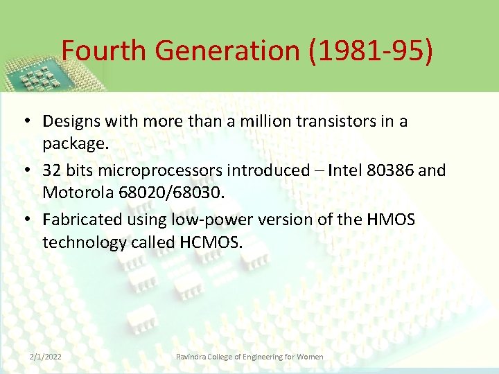
Fourth Generation (1981 -95) • Designs with more than a million transistors in a package. • 32 bits microprocessors introduced – Intel 80386 and Motorola 68020/68030. • Fabricated using low-power version of the HMOS technology called HCMOS. 2/1/2022 Ravindra College of Engineering for Women
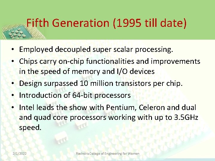
Fifth Generation (1995 till date) • Employed decoupled super scalar processing. • Chips carry on-chip functionalities and improvements in the speed of memory and I/O devices • Design surpassed 10 million transistors per chip. • Introduction of 64 -bit processors • Intel leads the show with Pentium, Celeron and dual and quad core processors working with up to 3. 5 GHz speed. 2/1/2022 Ravindra College of Engineering for Women
General Purpose Processors - Comparison 2/1/2022 Ravindra College of Engineering for Women
Classification of Microprocessors • Microprocessors can be classified based on their purpose, architecture, specifications and applications. • Based on the size of the data that the microprocessor can handle, they are classified as 4 -bit, 8 -bit, 16 -bit, 32 bit and 64 -bit microprocessors. • Based on the application of the processors, they are classified as i) General purpose processors, ii) Microcontrollers and iii) Special purpose processors. 2/1/2022 Ravindra College of Engineering for Women
General Purpose Processors • General purpose processors are those which are used in general computer system integration and can be used by the programmer for any application. • Common microprocessor such as Intel 8085 to Intel Pentium processors are examples of general purpose processors. • Microcontrollers are the microprocessor chips with in built hardware for the memory and ports. • These chips are can be programmed by the user for any generic control applications. 2/1/2022 Ravindra College of Engineering for Women
Special Purpose Processors • Special purpose processors are designed specifically to handle special functions required for an application. • The digital signal processors are examples for the special purpose processors and these have special instructions to handle signal processing. • The Application Specific Integrated Circuits (ASIC) chips are also the examples of this category of microprocessors. 2/1/2022 Ravindra College of Engineering for Women
Classification of microprocessors • Based on the architecture and hardware of the processors, they are classified as a)RISC processors, b)CISC processors, c)VLIW processors and d)Superscalar processors. • Reduced Instruction Set Architecture’, is a processor architecture that supports limited or small number of machine language instructions. 2/1/2022 Ravindra College of Engineering for Women
Classification of microprocessors • RISC processors can execute the programs faster than CISC processors. • CISC – Complex Instruction Set Computing architecture a) CISC processors have about 70 to few hundred instructions and are easier to program. b) CISC processors are slower and more expensive than RISC processors. c) Very Long Instruction Word (VLIW) processors have instruction composed of many machine operations which can be executed in parallel. 2/1/2022 Ravindra College of Engineering for Women
Classification of microprocessors • This is achieved by many functional units operating in parallel. • It has large number of registers and instruction level parallelism is achieved. • Superscalar processors are using complex hardware to achieve parallelism. • It is possible to have overlapping of execution of instructions in order to increase the speed of execution. 2/1/2022 Ravindra College of Engineering for Women
Memory Unit – An Introduction • Memory unit is the integral part of any microcomputer system and its primary purpose is to hold program and data. • The major design goal of memory unit is to allow it to operate at a speed close to that of the processor. • The cost factor inhibits the design of entire memory unit with single technology that guarantees high speed. • In order to seek a trade-off between the cost and operating speed, a memory system is usually designed with different technologies such as solid state, magnetic and optical. 2/1/2022 Ravindra College of Engineering for Women
Memory Unit – An Introduction • A microcomputer memory can be logically divided into four groups a) Processor memory/ register b) Cache memory c) Primary or Main Memory d) Secondary memory 2/1/2022 Ravindra College of Engineering for Women
Memory Unit – An Introduction • Processor Memory refers to a set of CPU registers. Processor registers are the first set of storage device available for the programmers to store any data. • But they are generally few in number up to about few tens to hundreds. • As these registers are available within the processor, they are the fastest memory registers. • The main disadvantage is the cost involved which forces to restrict the number to very few registers of few bytes. 2/1/2022 Ravindra College of Engineering for Women
Memory Unit – An Introduction • Cache memory is the fastest external memory to the processor and they are placed close to the processor. • The instructions to be executed are placed in cache memory for access by the processor. These are in few kilobytes in size. • These are semiconductor RAMs and are volatile. • The processor will fetch the next instruction from the cache memory and if the instruction is not in cache, it will refer to primary memory. 2/1/2022 Ravindra College of Engineering for Women
Memory Unit – An Introduction • Primary memory is the storage area from which all the programs are executed. • All the programs and corresponding data must be within primary memory prior to execution. • The size of primary memory is much larger compared to processor memory and cache memory but its operating speed is slower than them. • The primary memory in a system varies from few Kilobytes to about 1 Megabyte. 2/1/2022 Ravindra College of Engineering for Women
Memory Unit – An Introduction • Secondary memory refers to the storage medium for huge files such as program source codes, compilers, operating systems etc. • These are not accessed directly and very frequently by the microprocessor in a computer system. • They comprises of slow devices such as magnetic tapes and optical disks. • Sometimes they are referred to as auxiliary or backup store. 2/1/2022 Ravindra College of Engineering for Women
Memory Unit – An Introduction • Stored information in a magnetic tape or magnetic disk is not lost when the power is turned off. • Therefore these storage devices are called nonvolatile memories. 2/1/2022 Ravindra College of Engineering for Women
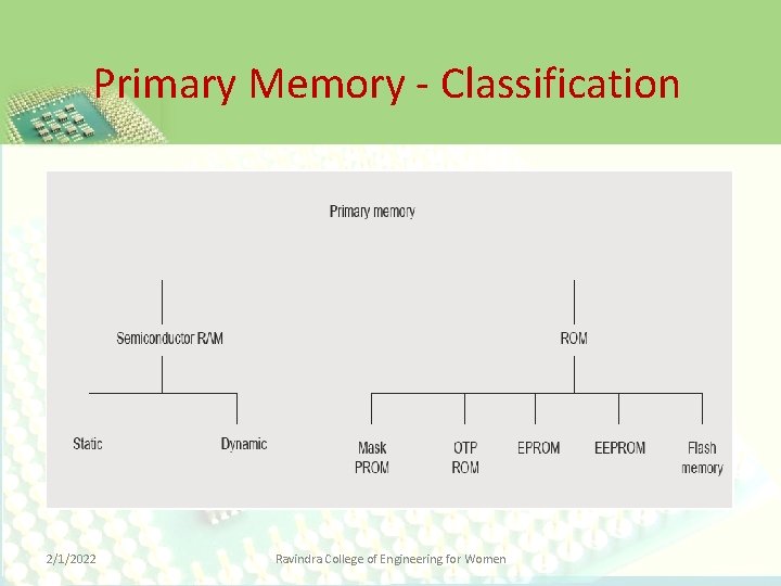
Primary Memory - Classification • Primary memory normally includes ROM (Read Only Memory) and RAM (Random Access Memory). • Microprocessor based systems have at least one RAM and ROM chips in it. • Information stored in semiconductor random access memories RAM will be lost if the power is turned off. • This property is known as volatility and hence, RAMs are usually called volatile memories. • ROM is a nonvolatile memory. 2/1/2022 Ravindra College of Engineering for Women
Primary Memory - Classification 2/1/2022 Ravindra College of Engineering for Women
Primary Memory - Classification • As the name implies, a ROM permits only a read access. There are many kinds of this category. • Mask Programmable ROMS are custom made for the customer and their contents are programmed by the manufacturer. • Since they are mass produced, they are inexpensive. The customer can not erase or program it afterwards. • Programmable ROMs are the devices which can be programmed by the user at the user’s place or field. • The main disadvantage of PROMs is that they cannot be erased and reprogrammed 2/1/2022 Ravindra College of Engineering for Women
EPROM • Erasable and Programmable ROMs (EPROMs) allow the erasure and reprogramming of the content by the user. • In an EPROM, programs are entered using electrical impulses and the stored information is erased using UV rays. 2/1/2022 Ravindra College of Engineering for Women
EPROM • Electrically Erasable PROMs (EEPROMs) or Electrically Alterable ROMs (EAROMs) allow the users to erase its contents by electrical means and also reprogramming by electrical signals. • EEPROMs are different from RAMs in the electrical signal required to erase and program. EEPROMs require a higher voltage for erasing and programming other than the normal 5 V supply. 2/1/2022 Ravindra College of Engineering for Women
Static RAM • In a semiconductor memory constructed using bipolar transistors, the information is stored in the form of voltage levels in flip-flops. • Such memories are called static RAMs because stored information remains constant for some period of time. • Static RAM maintains information in active circuits, power is required even when the chip is inactive or standby mode. • Hence, static RAMs require large power supplies. • Also each static RAM cell is about four times larger in area than an equivalent dynamic cell. 2/1/2022 Ravindra College of Engineering for Women
Dynamic RAM • Semiconductor memories designed using MOS transistors, the information is held in the form of electrical charges in capacitors. • the stored charge has the tendency of get leaked away. These memories are referred to as dynamic RAMs. • In order to prevent any information loss, dynamic RAMS have to be refreshed at regular intervals. Refreshing means boosting the signal level and writing it back. • This activity is performed using a hardware unit called “refresh logic”. 2/1/2022 Ravindra College of Engineering for Women
Differences 2/1/2022 Ravindra College of Engineering for Women
Input and Output Devices • The input/output or I/O section allows the computer to take in data from the outside world or send data to the outside world. • Peripherals such as keyboards, video display terminals, printers, and modems are connected to the I/O section. • These allow the user and the computer to communicate with each other. • The actual physical devices used to interface the computer buses to external systems are often called ports. 2/1/2022 Ravindra College of Engineering for Women
Function of I/O Ports • An input port allows data from a keyboard, an A/D converter, or some other source to be read into the computer under control of the CPU. • An output port is used to send data from the computer to peripheral devices, such as a video display terminal, a printer, or a D/A converter. 2/1/2022 Ravindra College of Engineering for Women
Function of I/O Ports • Simplest type of input or output port is just a set of parallel D flip-flops. • If they are being used as an input port, the D inputs are connected to the external device, and the Q outputs are connected to the data bus which can take the data to the CPU. • Data will then be transferred to the data bus when they are enabled by a control signal from the CPU. 2/1/2022 Ravindra College of Engineering for Women
Function of I/O Ports • In a system, where they are being used as an output port, the D inputs of the latches are connected to the data bus, and the Q outputs are connected to some external device. • Data sent out on the data bus by the CPU will be transferred to the external device when the latches are enabled by a control signal from the CPU. 2/1/2022 Ravindra College of Engineering for Women
Input Devices • Input devices include typewriter-like keyboards; hand-held devices such as the mouse, trackball, joystick, and special pen with pressure-sensitive pad; and microphones. • The simplest input device is a switch. • Input devices can also be sensors that provide information about their environment temperature, pressure, and so forth to a computer. • Another direct-entry mechanism is the optical laser scanner (e. g. , scanners used with point-of-sale terminals in retail stores) that can read bar-coded data or optical character fonts. 2/1/2022 Ravindra College of Engineering for Women
Output Devices • An output is any device through which the user can receive the results from the computer. • The output can be any display which can be changing fast or hard copies print out. Some other forms of output are sounds and alarms. • The simplest output devices used in almost all microprocessor based systems or computer systems are the LEDs or the seven segment LED displays and LCD displays. 2/1/2022 Ravindra College of Engineering for Women
Output Devices • The advanced video display terminals (either cathode-ray tubes or liquid crystal displays), ink-jet and laser printers, are the common output devices nowadays. • Some output devices can be used to directly control machineries. • Some devices, such as display terminals with touch screen, may provide both input and output. • Modems and other network interface cards can also be called as output devices as they enable the transmission and reception of data between computers. 2/1/2022 Ravindra College of Engineering for Women
Technological Improvements • Technology improvements are taking place fast in the microprocessor, microcomputer and personal computer systems. • The technical and research improvements in the field of microprocessor technology is listed below. – Increase in data bus / address bus width. The processing capability of the microprocessor can be drastically improved by increasing data size 2/1/2022 Ravindra College of Engineering for Women
Technological Improvements • Increase in speed a) As the data to be processed by the microprocessors and computers increased in volume, it became a necessity to increase the speed of the processor. b) By high speed processors, the user can get the results faster even with the large data volumes. 2/1/2022 Ravindra College of Engineering for Women
Technological Improvements • Reduction in size and increase in capability a) The trend in microprocessor technology is to include large amount of peripherals such as memory and I/O ports within a single chip. b) Microcontrollers are manufactured by all semiconductor manufacturers in this aspect. c) Development in the processing of large scale integration has lead to small chips of microprocessors with large built in peripherals. d) We have now processors with large amount of flash memory available. Ravindra in the market. 2/1/2022 College of Engineering for Women
Technological Improvements • Development of external peripherals a) The use of computers in all the fields have resulted in the development of many fast and advanced peripheral devices to be interfaced with the microprocessor. b) For example, applications of microprocessors in medical field has resulted in many handheld electronic devices with the specialized input sensors and output printers etc. c) The faster peripherals can increase the speed of processor execution and a good user interface. 2/1/2022 Ravindra College of Engineering for Women
Technological Improvements • Increase in memory size and speed a) The developments in the Integrated circuit technology have lead to developments in the reduction of the memory size and the increase in memory speed. b) This reduces the memory access time of the processor and so will result in the higher speed of execution. c) Also more amount of memory per unit area is possible 2/1/2022 Ravindra College of Engineering for Women
Technological Improvements • The microprocessors are largely used in handheld devices operated from the battery source. • This has resulted in the research towards reduction of power consumption in the microprocessor chips. • As power consumption is reduced, the devices can work for more time with one full charge of batteries. • There are many devices operating at 3. 3 V are even lower and have low power consumption. 2/1/2022 Ravindra College of Engineering for Women
Summary • Microprocessor is an electronic circuit that functions as the central processing unit (CPU) of a computer, providing computational control. • The microprocessor is the controlling element in a computer system. • The microprocessor performs data transfers, does simple arithmetic and logic operations, and makes simple decisions 2/1/2022 Ravindra College of Engineering for Women
Summary • The basic operation of the microprocessor is to fetch instructions stored in the memory and execute them one y one in sequence. • Microprocessors are used in almost all advanced electronic systems • Microcontrollers are advanced forms of microprocessors with memory and ports present within the chip 2/1/2022 Ravindra College of Engineering for Women
Summary • A microcomputer system is made y interfacing memory and I/O devices to a microprocessor • Microprocessor evolution is classified into five generations • The processors that are currently in use belong to the fifth generation. 2/1/2022 Ravindra College of Engineering for Women
Chapter 3 INTEL 8086 MICROPROCESSOR ARCHITECTURE, FEATURES, & SIGNALS 2/1/2022 Ravindra College of Engineering for Women
Introduction • 1978 - Intel released its first 16 -bit microprocessor - 8086 executes the instructions at 2. 5 MIPS (i. e 2. 5 million Instruction per second). • execution time of one instruction - 400 ns (=1/MIPS=1/(2. 5 x 10⁶)) • 8086 can also address one megabytes (1 MB=220 bytes) of memory. • Another feature in 8086 - presence of a small 6 -byte instruction queue - so instructions fetched from memory are placed in it before they are executed. • higher execution speed - larger memory size 2/1/2022 Ravindra College of Engineering for Women
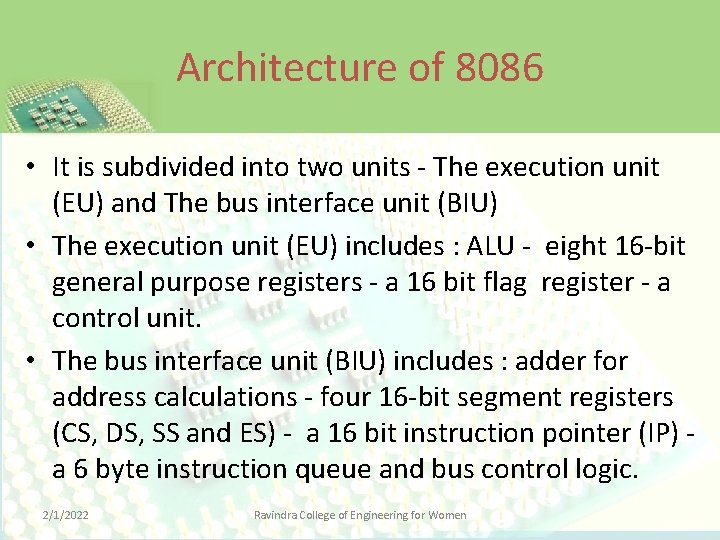
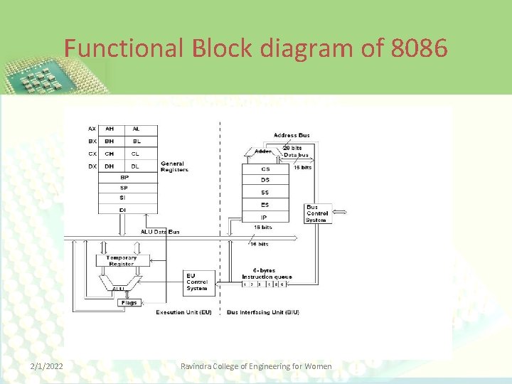
Architecture of 8086 • It is subdivided into two units - The execution unit (EU) and The bus interface unit (BIU) • The execution unit (EU) includes : ALU - eight 16 -bit general purpose registers - a 16 bit flag register - a control unit. • The bus interface unit (BIU) includes : adder for address calculations - four 16 -bit segment registers (CS, DS, SS and ES) - a 16 bit instruction pointer (IP) a 6 byte instruction queue and bus control logic. 2/1/2022 Ravindra College of Engineering for Women
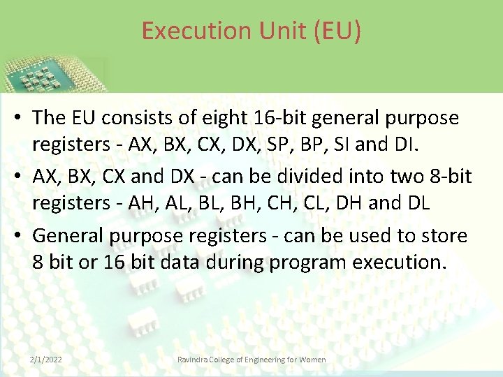
Execution Unit (EU) • The EU consists of eight 16 -bit general purpose registers - AX, BX, CX, DX, SP, BP, SI and DI. • AX, BX, CX and DX - can be divided into two 8 -bit registers - AH, AL, BH, CL, DH and DL • General purpose registers - can be used to store 8 bit or 16 bit data during program execution. 2/1/2022 Ravindra College of Engineering for Women
Functional Block diagram of 8086 2/1/2022 Ravindra College of Engineering for Women
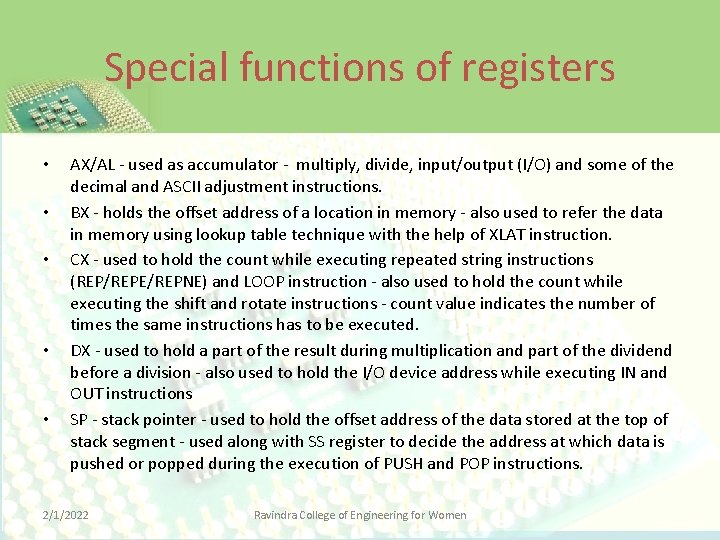
Special functions of registers • • • AX/AL - used as accumulator - multiply, divide, input/output (I/O) and some of the decimal and ASCII adjustment instructions. BX - holds the offset address of a location in memory - also used to refer the data in memory using lookup table technique with the help of XLAT instruction. CX - used to hold the count while executing repeated string instructions (REP/REPE/REPNE) and LOOP instruction - also used to hold the count while executing the shift and rotate instructions - count value indicates the number of times the same instructions has to be executed. DX - used to hold a part of the result during multiplication and part of the dividend before a division - also used to hold the I/O device address while executing IN and OUT instructions SP - stack pointer - used to hold the offset address of the data stored at the top of stack segment - used along with SS register to decide the address at which data is pushed or popped during the execution of PUSH and POP instructions. 2/1/2022 Ravindra College of Engineering for Women
Special functions of registers • BP - Base Pointer - used to hold the offset address of the data to be read from or write into the stack segment • SI - Source Index register - used to hold the offset address of source data in data segment while executing string instructions • DI - Destination Index register - used to hold the offset address of destination data in extra segment while executing String instructions. • NOTE : segment - a portion of memory where data for a program is stored the maximum size of a segment can be 64 bytes - minimum size of a segment can be even one byte - segment begins in memory at a memory address which is divisible by 16. 2/1/2022 Ravindra College of Engineering for Women
Flag register of 8086 • The flags - classified into status flags and control flags • CF, PF, AF, ZF, SF and OF - status flags - they indicate the status of the result that is obtained after the execution of arithmetic or logic instruction • DF, IF and TF - control flags - they can control the operation of CPU 2/1/2022 Ravindra College of Engineering for Women
Function of different flags • • • CF (Carry Flag) - holds the carry after 8 bit or 16 bit addition - holds borrow after 8 bit or 16 bit subtraction performed PF (Parity Flag) - If the lower 8 bit of the result is having odd parity (i. e. odd number of 1 s) - PF is set to 0 - PF is set to 1 if the lower 8 bit of result is having even parity. AF (Auxiliary Carry Flag) - holds the carry after addition - the borrow after subtraction of the bits in bit position 3 - (LSB is treated as bit position 0) - used by DAA and DAS instructions to adjust the value in AL after a BCD addition or subtraction. ZF (Zero Flag) - indicates that the result of an arithmetic or logic operation is zero If Z=1, the result is zero - if Z=0, the result is not zero. SF (Sign flag) - holds the arithmetic sign of the result after an arithmetic or logic instruction is executed - If S-0, the sign bit is 0 and the result is negative. 2/1/2022 Ravindra College of Engineering for Women
Function of different flags • TF (Trap Flag) - used to debug a program usingle step technique - If T flag is set (i. e. TF=1) - 8086 gets interrupted (Trap or single step interrupt) after the execution of each instruction in the program - If TF is cleared (i. e. TF=0) - the trapping or debugging feature is disabled • DF (Direction Flag) - selects either the increment or decrement made for the DI and/or SI register during the execution of string instructions - If D=0 - registers are automatically incremental - if D=1 - the register are automatically decremented - can set or cleared using the STD or CLD instruction respectively. 2/1/2022 Ravindra College of Engineering for Women
Function of different flags • • IF (Interrupt Flag) - controls the operation of the ‘INTR’ interrupt pin of 8086 - If I=0 - INTR pin is disabled - if I=1 - INTR pin is enabled - I flag can be set or cleared using the instruction STI or CLI respectively. OF (Overflow flag) - Signed numbers are represented in 2’s complement form when the number is negative in microprocessor - When signed numbers are added or subtracted - overflow may occur - indicating that the result has exceeded the capacity of the machine - For example if the 8 -bit signed data 7 EH (= +126) is added with the 8 -bit signed data 02 H(= +2), the result is 80 H(= -128 in 2’s complement form). This result indicates an overflow condition - overflow flag is set during the above signed addition - In an 8 -bit register, the minimum and maximum value of the signed number that can be stored in -128 (=80 H) and +127 (=7 FH) respectively - In a 16 bit register, the minimum and maximum value of the signed number that can be stored is -32768 (=8000 H) and +32767 (=7 FFFH) respectively For operation an unsigned data, OF is ignored. 2/1/2022 Ravindra College of Engineering for Women
Bus Interface Unit (BIU) • There are four segment registers - CS, DS, SS and ES. • The function of the CS, DS, SS and ES register - indicate the starting address or base address of code segment, data segment, stack segment and extra segment in memory • The code segment - contains the instructions of a program - data segment contains - data for the program • The stack segment - holds the stack of a program - which is needed while executing CALL and RET instructions - also to handle interrupts - extra segment - additional data segment - used by some of the string instructions - minimum size of a segment - one byte - maximum size of a segment is 64 Kbytes. • The base address - can be obtained by adding four binary 0 s to the right most portion of the content of corresponding segment register which is same as adding a hexadecimal digit 0 to the right most portion of a segment register. 2/1/2022 Ravindra College of Engineering for Women
Bus Interface Unit (BIU) • If the size of two different segments is less than 64 Kbytes then it is possible for two segments to get overlapped (i. e. within 64 Kbytes allocated to a segment, another segment can start). • Let a particular application in 8086 requires code segment of 1 Kbyte size and data segment of 2 Kbytes size. If the code segment is stored in memory from the address 20000 H then it will end at the memory address 203 FFH. • The data segment can be stored from the address 20400 H (which is the immediate next 16 -byte boundary in memory). • The CS and DS registers are loaded with the value 2000 H and 2040 H respectively for running this application in 8086. 2/1/2022 Ravindra College of Engineering for Women
Accessing memory locations • Each address in physical memory (ROM/EPROM chips) is known as physical address. In order to access an operand (either data or instruction) from memory from a particular segment, 8086 has to first calculate the physical address of that operand. • To find the physical address of that operand, the 8086 adds the base address of the corresponding segment with an offset address which may be either the content of a register or an 8 bit or 16 bit displacement given in the instruction or combination of both, depending upon the addressing mode used by the instruction. • The 8086 designers have assigned certain register(s) as default offset register(s) for certain segment register. • But this default assignment can be changed by using segment override prefix in the instruction which is explained in the next chapter (section 14. 2). 2/1/2022 Ravindra College of Engineering for Women
Fetching of an instruction from memory • Let us assume that the CS register is having the value 3000 H and the IP register is having the value 2000 H. • To fetch an instruction from memory, the CPU calculates the memory address from where the next instruction is to be fetched, as shown below: • CS X 10 H =30000 H + Base address of code segment • IP = 2000 H Offset address • 32000 H Memory address from where next instruction is taken by CPU 2/1/2022 Ravindra College of Engineering for Women
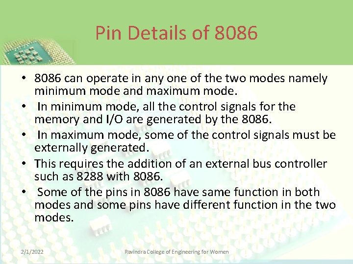
Pin Details of 8086 • 8086 can operate in any one of the two modes namely minimum mode and maximum mode. • In minimum mode, all the control signals for the memory and I/O are generated by the 8086. • In maximum mode, some of the control signals must be externally generated. • This requires the addition of an external bus controller such as 8288 with 8086. • Some of the pins in 8086 have same function in both modes and some pins have different function in the two modes. 2/1/2022 Ravindra College of Engineering for Women
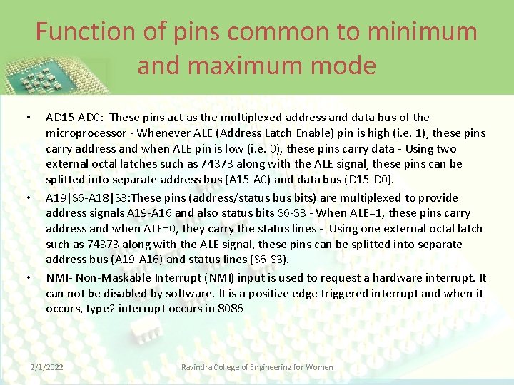
Function of pins common to minimum and maximum mode • • • AD 15 -AD 0: These pins act as the multiplexed address and data bus of the microprocessor - Whenever ALE (Address Latch Enable) pin is high (i. e. 1), these pins carry address and when ALE pin is low (i. e. 0), these pins carry data - Using two external octal latches such as 74373 along with the ALE signal, these pins can be splitted into separate address bus (A 15 -A 0) and data bus (D 15 -D 0). A 19|S 6 -A 18|S 3: These pins (address/status bits) are multiplexed to provide address signals A 19 -A 16 and also status bits S 6 -S 3 - When ALE=1, these pins carry address and when ALE=0, they carry the status lines - Using one external octal latch such as 74373 along with the ALE signal, these pins can be splitted into separate address bus (A 19 -A 16) and status lines (S 6 -S 3). NMI- Non-Maskable Interrupt (NMI) input is used to request a hardware interrupt. It can not be disabled by software. It is a positive edge triggered interrupt and when it occurs, type 2 interrupt occurs in 8086 2/1/2022 Ravindra College of Engineering for Women
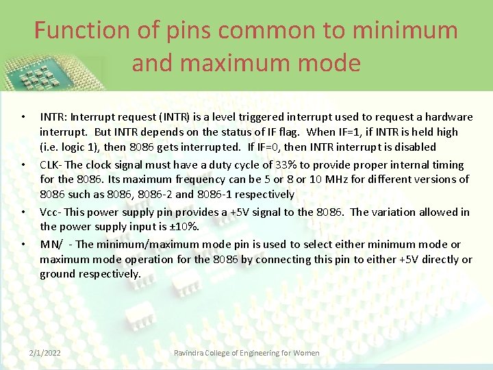
Function of pins common to minimum and maximum mode • • INTR: Interrupt request (INTR) is a level triggered interrupt used to request a hardware interrupt. But INTR depends on the status of IF flag. When IF=1, if INTR is held high (i. e. logic 1), then 8086 gets interrupted. If IF=0, then INTR interrupt is disabled CLK- The clock signal must have a duty cycle of 33% to provide proper internal timing for the 8086. Its maximum frequency can be 5 or 8 or 10 MHz for different versions of 8086 such as 8086, 8086 -2 and 8086 -1 respectively Vcc- This power supply pin provides a +5 V signal to the 8086. The variation allowed in the power supply input is ± 10%. MN/ - The minimum/maximum mode pin is used to select either minimum mode or maximum mode operation for the 8086 by connecting this pin to either +5 V directly or ground respectively. 2/1/2022 Ravindra College of Engineering for Women
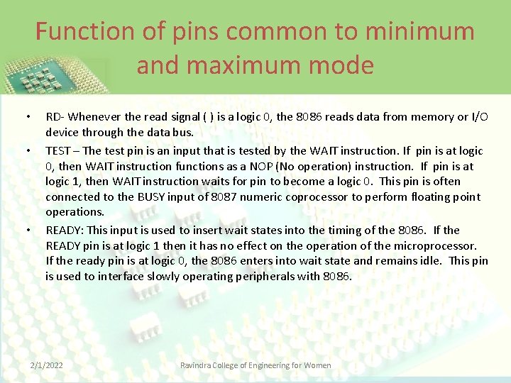
Function of pins common to minimum and maximum mode • • • RD- Whenever the read signal ( ) is a logic 0, the 8086 reads data from memory or I/O device through the data bus. TEST – The test pin is an input that is tested by the WAIT instruction. If pin is at logic 0, then WAIT instruction functions as a NOP (No operation) instruction. If pin is at logic 1, then WAIT instruction waits for pin to become a logic 0. This pin is often connected to the BUSY input of 8087 numeric coprocessor to perform floating point operations. READY: This input is used to insert wait states into the timing of the 8086. If the READY pin is at logic 1 then it has no effect on the operation of the microprocessor. If the ready pin is at logic 0, the 8086 enters into wait state and remains idle. This pin is used to interface slowly operating peripherals with 8086. 2/1/2022 Ravindra College of Engineering for Women
Function of pins common to minimum and maximum mode • RESET: This input causes the 8086 to reset if it is held at logic 1 for a minimum of four clocking periods. Whenever the 8086 is reset, the CS and IP are initialized to FFFFH and 0000 H respectively and all other registers are initialized with the value 0000 H. This causes 8086 to begin executing instructions from the memory address FFFF 0 H. • GND: The GND connection is the return for the power supply (Vcc). 8086 has two GND pins and both must be connected to ground for properation. 2/1/2022 Ravindra College of Engineering for Women
Function of pins used in minimum mode • • • M/IO : The M/ pin selects memory or I/O. This pin indicates whether the 8086 performs memory read or write operation (M/IO =1) or I/O read or write operation (M/ =0). WR: The write signal indicates that 8086 is sending data to a memory or I/O device. When DR is at logic 0, the data bus contains valid data for memory or I/O. DT/ R: The data transmit/receive signal shows that the 8086 data bus is transmitting (DT/ R=1) or receiving (DT/R =0) data. This signal is used to control the data flow direction in external data bus buffers. DEN: Data bus enable signal activates external data bus buffers. When data is transferred through the data bus of 8086, this signal is at logic 0. When it is high, no data flows in the data bus. ALE: When Address Latch Enable (ALE) signal is high, it indicates that the 8086 multiplexed address/data bus (AD 15 -AD 0) and multiplexed address/status bus (A 19/S 6 -A 16/S 3) contain address which can be either memory address on I/O port address. 2/1/2022 Ravindra College of Engineering for Women
Function of pins used in minimum mode • INTA: The interrupt acknowledge signal is a response to the INTR input pin. The INTA signal is used to place the interrupt type or vector number into the data bus in response to INTR interrupt. • HOLD: The hold input requests a direct memory access (DMA) and is generated by DMA controller. If the HOLD signal is logic 1, the 8086 completes the execution the current instruction and places its address data and control bus at the high impedance state. If the HOLD pin is at logic 0, the 8086 executes the instructions normally. • HLDA: Hold acknowledgement signal indicates that the 8086 has entered the hold state and is connected to HLDA input of DMA controller. 2/1/2022 Ravindra College of Engineering for Women
Function of pins used in Maximum mode • S 2, S 1, S 0 : The states bits indicates the function of the current bus cycle. These signals are normally decoded by the 8288 (bus controller). Figure 13. 10 shows the function of these three status bits in the maximum mode. • LOCK: The lock output is used to lock peripherals off the system. This pin is activated by using the LOCK prefix on any instruction. • RQ/GT 0 and RQ/GT 1 : The request/grant pins request DMA during maximum mode operation of 8086. These lines are both bi-directional and are used to request and grant for a DMA operation. • QS 1 and QS 0: The queue status bits show the status of the internal instruction queue in 8086. These pins are provided for access by the numeric coprocessor (8087). Figure 13. 11 shows the function of QS 1 and QS 0 bits. 2/1/2022 Ravindra College of Engineering for Women
Summary • • • The internal architecture of 8086 mainly contains two units namely bus interface unit (BIU) and execution unit (EU). The BIU takes care of fetching the instructions and data from memory into the processor using the content of a segment register and offset. There exists a 6 -byte instruction queue in 8086 which is used to store the recently fetched instructions into the CPU. This is used to speed up the execution of a program. There are four memory segments namely code, data, stack, extra segments in 8086 and their base address is indicated by adding four binary 0 s to the right of the corresponding segment register’s content. The maximum size of a memory segment is 64 Kbytes. For fetching either an instruction byte or data, 8086 adds the base address of the particular segment with an offset address present either in a register or given as 8 or 16 bit displacement in the instruction or combination of both. 2/1/2022 Ravindra College of Engineering for Women
Summary • The 8086’s designer have already fixed up default offset register(s) for every segment register. But this can be changed using segment override prefix in the instruction. • The EU contains the ALU, general purpose registers and flag register which are used during the execution of an instruction. • The flag register contain different flags which can be classified into status flags and control flags. The status flags reflect the result of arithmetic or logical operation and the control flags control the operation during execution of instructions. • 8086 can be operated in minimum mode or maximum mode. • The address bus and data bus size are 20 bits and 16 bits respectively in 8086. The 8086 can access maximum memory size of 1 Mbytes (=220) as it has 20 bit address bus. 2/1/2022 Ravindra College of Engineering for Women
Key terms • • Execution unit (EU) includes the ALU, eight 16 -bit general purpose registers, a 16 bit flag register and control unit in 8086. This unit is responsible for executing the instructions in 8086. Bus interface unit (BIU) includes an adder for address calculations, four 16 -bit segment registers (CS, DS, SS and ES), a 16 bit instruction pointer (IP), a 6 byte instruction queue and bus control logic. This unit is responsible for fetching the instruction and data into 8086 from memory or I/O device. Code segment contains the instructions of a program Data segment contains data for the program Stack segment holds the stack of a program Extra segment is an additional data segment and is also used by some of the string instructions. Segment Register indicates the starting or base address of a segment in memory. Offset is a 16 -bit number that is added to the base address of a segment to select a byte of instruction or data from memory. 2/1/2022 Ravindra College of Engineering for Women
Key terms • Flags show information related to the result of arithmetic or logic operation held in ALU. Flags in the flag registers can be classified into status flags and control flags. • Instruction queue is 6 -bytes long and it stores the pre-fetched instructions from the memory and is used to speed up the execution of a program. • Minimum mode operation – In this mode, all the control signals for the memory and I/O are generated by the microprocessor itself • Maximum mode operation – In this mode, some of the control signals must be externally generated using bus controller such as 8288. • Re-locatable program - A re-locatable program is one which can be placed anywhere in the memory map of 8086 and executed without any modification in the program. 2/1/2022 Ravindra College of Engineering for Women