Chapter 1 Introduction to HCS 12MC 9 S


 • Random-access memory (RAM): same amount of time is")
 • Erasable programmable ROM (EPROM) – Electrically programmable many")


 • Used only by branch instructions • Short and")
 • For example, minus … … bmi minus …")

 • 5 -bit Constant Offset Indexed Addressing – The")
 • 16 -bit Constant Offset Indexed Addressing – The")


 • Transfer instructions copy the contents of")
 • The EXG instruction exchanges the contents")


- Slides: 39
Chapter 1 Introduction to HCS 12/MC 9 S 12
What is a Computer? • Software • Hardware Computer Hardware Organization
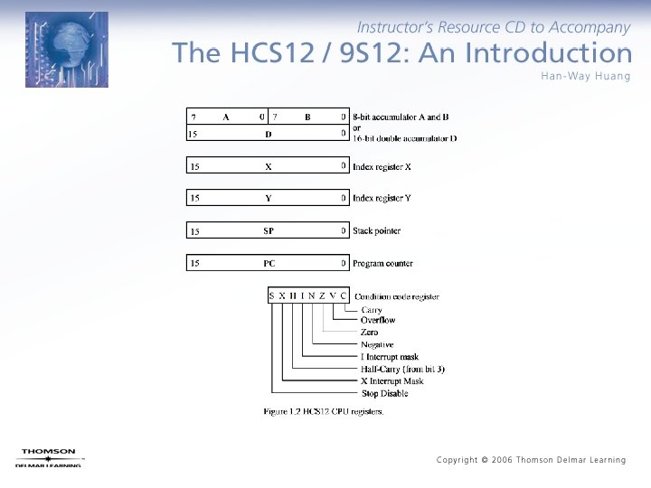
The Processor • • • Registers – Storage locations in the processor Arithmetic logic unit Control unit – Program counter keeps track of the address of the next instruction to be executed. – Status register flags the instruction execution result. • • The microprocessor – A processor implemented on a very large scale integration (VLSI) chip – Peripheral chips are needed to construct a product The microcontroller – The processor and peripheral functions implemented on one VLSI chip
Features of the HCS 12 Microcontroller • 16 -bit CPU • 64 KB memory space (also supports expanded memory up to 1 MB through a 16 -KB window) • 0 KB to 4 KB of EEPROM • 2 KB to 14 KB of on-chip SRAM • 32 KB to 512 KB flash memory • Sophisticated timer functions that include: input capture, output compare, pulse accumulators, real-time interrupt, and COP timer • Serial communication interfaces: SCI, SPI, CAN, BDLC • Background debug mode (BDM) • 10 -bit A/D converter • Instructions for supporting fuzzy logic function
Semiconductor Memory (1 of 2) • Random-access memory (RAM): same amount of time is required to access any location on the same chip – Dynamic random-access memory (DRAM): periodic refresh is required to maintain the contents of a DRAM chip – Static random-access memory (SRAM): no periodic refresh is required • Read-only memory (ROM): can only be read but not written by the processor – Mask-programmed read-only memory (MROM): programmed when being manufactured – Programmable read-only memory (PROM): is fuse-based, can be programmed by the end user by a burner.
Semiconductor Memory (2 of 2) • Erasable programmable ROM (EPROM) – Electrically programmable many times – Erased by ultraviolet light (through a window) – Erasable in bulk (whole chip in one erasure operation) • Electrically erasable programmable ROM (EEPROM) – Electrically programmable many times – Electrically erasable many times – Can be erased one location, one row, or whole chip in one operation • Flash memory – Electrically programmable many times – Electrically erasable many times – Can only be erased in bulk or a sector at a time
Computer Software • Computer programs are known as software. • A program is a sequence of instructions. • Machine instruction – A sequence of binary digits which can be executed by the processor • 0001 1000 0110: A [A] + [B] • 0100 0011: A [A] + 1 • 1000 0110 0000 0110: A 6 – Hard to understand, enter, debug, and maintain for human being
Assembly Language • Defined by assembly instructions – An assembly instruction is a mnemonic representation of a machine instruction • ABA: A [A] + [B] • DECA: A [A] – 1 – Assembly programs must be translated into machine instructions before it can be executed -- translated by an assembler – There are two kinds of assemblers: native assembler and cross assembler. – Programmers need to work on the program logic at a very low level and cannot achieve high productivity.
High-level Language • Syntax of a high-level language is similar to English. • A translator is required to translate the program written in a highlevel language -- done by a compiler. – There are two types of compilers: native compiler and cross compiler. • High-level languages allow the user to work on the program logic at higher level and achieve higher productivity. • Source code – A program written in assembly or high-level language • Object code – The output of an assembler or compiler
line addr. 1: machine code source code = 00002000 org $2000 2: 2000 B 6 1000 ldaa $1000 3: 2003 BB 1001 adda $1001 4: 2006 BB 1002 adda $1002 5: 2009 7 A 1100 staa $1100 6: end
Memory Addressing • Memory consists of a sequence of directly addressable locations. – A location is referred to as an information unit. – A memory location can be used to store data, instruction, and the status of peripheral devices. – A memory location has two components: an address and its contents.
• Data transfers between the CPU and the memory are done over the common buses: address bus and data bus. • Notations: m[addr] represents the contents of a memory location, [reg] refers to the contents of a register. – For example, [$20] refers to the contents of memory location at $20. – [A] refers to the contents of accumulator A.
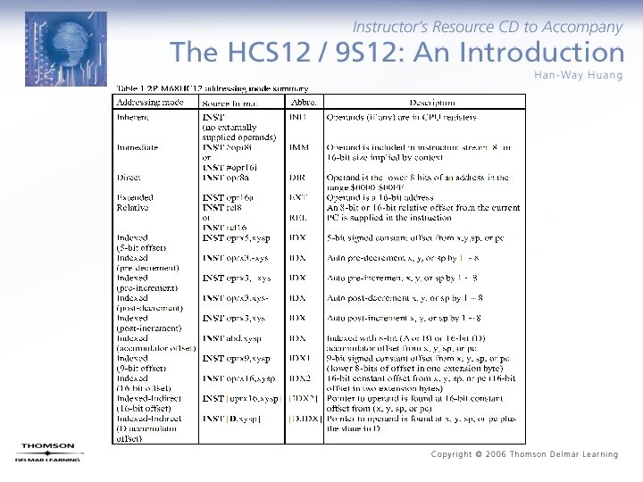
Addressing Modes • A HCS 12 instruction consists of one or two bytes of opcode and zero to five bytes of operand addressing information. – Opcode bytes specify the operation to be performed by the CPU. – The first byte of a two-byte opcode is always $18. • Addressing modes specify the operand to be operated on. • The addressing mode may specify a value, a register, or a memory location to be used as an operand.
Inherent Mode • Instructions that use this mode do not use extra bytes to specify operands because the instructions either do not need operands or all operands are CPU registers. – Operands are implied by the opcode. – Examples • NOP • INX • DECA
Immediate Mode • Operands for instructions that use immediate mode are included in the instruction. • CPU does not access memory for operands. • Example – LDAA #$55 – LDX #$1000
Direct Mode • This mode can only specify memory locations in the range of 0 - 255. • This mode uses only one byte to specify the operand address. • Example – LDAA $20 – LDAB $40
Extended Mode • In this mode, the full 16 -bit address is provided in the instruction. • For example, – LDAA $4000 – LDX $FE 60
Relative Mode (1 of 2) • Used only by branch instructions • Short and long conditional branch instructions use exclusively relative mode. • BRCLR and BRSET instructions can also use relative mode to specify branch target. – A short branch instructions consists of an 8 -bit opcode and a signed 8 -bit offset. – The short relative mode can specify a range of -128 ~ +127. – A long branch instruction consists of an 8 -bit opcode and a signed 16 -bit offset. – The range of the long relative mode is from -32768 ~ +32767. • A programmer uses a symbol to specify the branch target and the assembler will figure out the actual branch offset (distance) from the instruction that follows branch instruction.
Relative Mode (2 of 2) • For example, minus … … bmi minus …
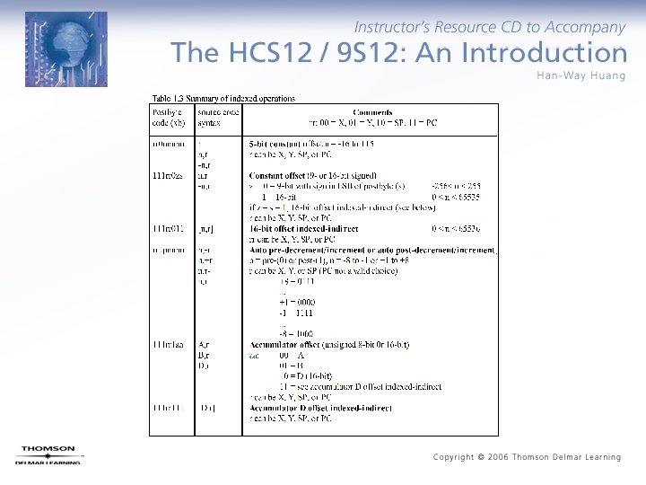
Indexed Mode • This mode uses the sum of an index register (X, Y, PC, or SP) and an offset to specify the address of an operand. – The offset can be a 5 -bit, 9 -bit, and 16 -bit signed value or the value in accumulator A, B, or D. – Automatic pre- or post-increment or pre- or postdecrement by -8 to +8 are options. – PC can be used as the index register for all but autoincrement or auto-decrement mode. – Indirect indexing with 16 -bit offset or accumulator D as the offset is supported. • A summary of indexed addressing modes is given in Table 1. 3.
Indexed Addressing (1 of 2) • 5 -bit Constant Offset Indexed Addressing – The base index register can be X, Y, SP, or PC. – The range of the offset is from -16 to +15. – Examples • ldaa 0, X • stab -8, 0 • 9 -bit Constant Offset Indexed Addressing – The base index register can be X, Y, SP, or PC. – The range of the offset is from -256 to +255. – Examples • ldaa $FF, X • ldab -20, Y
Indexed Addressing (2 of 2) • 16 -bit Constant Offset Indexed Addressing – The base index register can be X, Y, SP, or PC. – This mode allows access any location in the 64 -KB range. – Examples • ldaa 2000, X • staa 4000, Y • 16 -bit Constant Indirect Indexed Addressing – A 16 -bit offset is added to the base index register to form the address of a memory location that contains a pointer to the memory location affected by the instruction. – The square brackets distinguish this addressing mode from the 16 -bit constant offset indexing. • Example, – ldaa [10, X] – staa [20, Y]
Auto Pre/Post Decrement/Increment Indexed Addressing • The base index register can be X, Y, or SP. • The index register can be incremented or decremented by an integer value either before or after indexing taking place. • The index register retains the changed value after indexing. • The value to be incremented or decremented is in the ranges -8 thru -1 or 1 thru 8. • The value needs to be related to the size of the operand or the current instruction. • Examples – staa 1, -SP – staa 1, SP– ldx 2, +SP – ldx 2, SP+
Accumulator Offset Indexed Addressing • The effective address of the operand is the sum of the accumulator and the base index register. – The base register can be X, Y, SP, or PC. – The accumulator can be the 8 -bit A or B or the 16 -bit accumulator D. – Example • ldaa B, X • stab B, Y
Accumulator D Indirect Indexed Addressing The value in D is added to the value in the base index register to form the address of the memory location that contains the address to the memory location affected by the instruction. The square brackets distinguish this addressing mode from accumulator D offset indexing. Example jmp [D, PC] go 1 dc. w target 1 go 2 dc. w target 2 go 3 dc. w target 3 … target 1 … . target 2 … . target 3 …
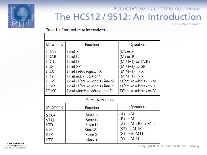
HCS 12 Instruction Examples • The LOAD and STORE instructions – The LOAD instruction copies the contents of a memory location or places an immediate value into an accumulator or a CPU register. – STORE instructions save the contents of a CPU register into a memory location. – N and Z flags of the CCR register are automatically updated and the V flag is cleared. • • All except for the relative mode can be used to select the memory location or value to be loaded into an accumulator or CPU register. All except for the relative and immediate modes can be used to select memory location to store contents of the CPU register. For example, – ldaa 0, X – staa $20 – stx $8000 – ldd #100
Transfer and Exchange Instructions (1 of 2) • Transfer instructions copy the contents of a CPU register or accumulator into another CPU register or accumulator. • TFR is the universal transfer instruction, but other mnemonics are accepted for compatibility with the 68 HC 11. • The TAB and TBA instructions affect the N, Z, and V condition code bits. • The TFR instruction does not affect any condition code bits. For example, – TFR D, X ; [D] X – TFR A, B ; [A] B – TFR A, X ; 0: [A] X ; upper 8 -bit of X is cleared to 0 – TFR X, A ; X[7: 0] A ; lower 8 bits copied to A
Transfer and Exchange Instructions (2 of 2) • The EXG instruction exchanges the contents of a pair of registers or accumulators. For example, exg A, B exg D, X exg A, X ; A X[7: 0], X $00: [A] exg X, B ; X $00: [B], B X[7: 0] • The SEX instruction sign-extend an 8 -bit two’s complement number into a 16 -bit number so that it can be used in 16 -bit signed operations. For example, SEX A, X
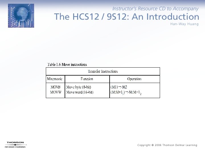
Move Instructions • These instructions move data bytes or words from a source to a destination in memory. • Six combinations of immediate, extended, and index addressing modes are allowed to specify the source and destination addresses: – IMM EXT, IDX EXT, IMM IDX, IDX – For example, • movb $100, $800 • movw 0, X, 0, Y EXT, EXT IDX,
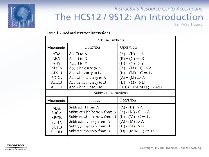
Add and Subtract Instructions • These instructions perform fundamental arithmetic operations. • The destinations of these instructions are always a CPU register or accumulator. • There are two-operand three-operand versions of these instructions. • Three-operand ADD or SUB instructions always include the C flag as one of the operand. • Three-operand ADD or SUB instructions are used to perform multi-precision addition or subtraction. • Example • adda $1000 ; A [A] + [$1000] • adca $1000 ; A [A] + [$1000] + C • suba $1002 ; A [A] + [$1002] • sbca $1000 ; A [A] - [$1000] - C
• Instruction Execution Cycle – One or more read cycles to fetch instruction opcode bytes and addressing information – One or more read cycles to fetch the memory operand (s) (optional) – Perform the operation specified by the opcode – One or more write cycles to write back the result to either a register or a memory location (optional) • Instruction Queue – The HCS 12 executes one instruction at a time and many instructions take several clock cycles to complete. – When the CPU is performing the operation, it does not need to access memory. • The HCS 12 prefetches instructions when the CPU is not accessing memory to speedup the instruction execution process. • There are two 16 -bit queue stages and one 16 -bit buffer. Unless buffering is required, program information is first queued in stage 1, and then advanced to stage 2 for execution.
Embedded System Any product that uses a microprocessor or microcontroller as its controller. Functionality is the focus not the processor itself. Weather Station
Other Examples of Embedded System • Cell phone: making the phone call, accepting incoming call, accessing Internet, displaying • Web page: handling input/output, keeping track of time, taking picture, and playing game • Home security system: sensing external temperature, smoke, humidity, and intruders; taking appropriate actions according to the detected events • Automobile: monitoring speed, gas level, temperature, distance, direction, and so on; controlling display, full injection, air bag deployment, cruising, and so on; giving warnings • Network router: responsible for message routing, congestion and traffic control, and so on