Chapter 1 Introduction EE 141 VLSI Test Principles









- Slides: 41

Chapter 1 Introduction EE 141 VLSI Test Principles and Architectures 1 Ch. 1 - Introduction - P.

What is this chapter about? q Introduce fundamental concepts and various aspects of VLSI testing q Focus on § Importance of testing in the design and manufacturing processes § Challenges in test generation and fault modeling § Levels of abstraction in VLSI testing q Provide overview of VLSI test technology EE 141 VLSI Test Principles and Architectures 2 Ch. 1 - Introduction - P.

Introduction to VLSI Testing Introduction q Testing During VLSI Life Cycle q Test Generation q Fault Models q Levels of Abstraction q Overview of Test Technology q Concluding Remarks q EE 141 VLSI Test Principles and Architectures 3 Ch. 1 - Introduction - P.

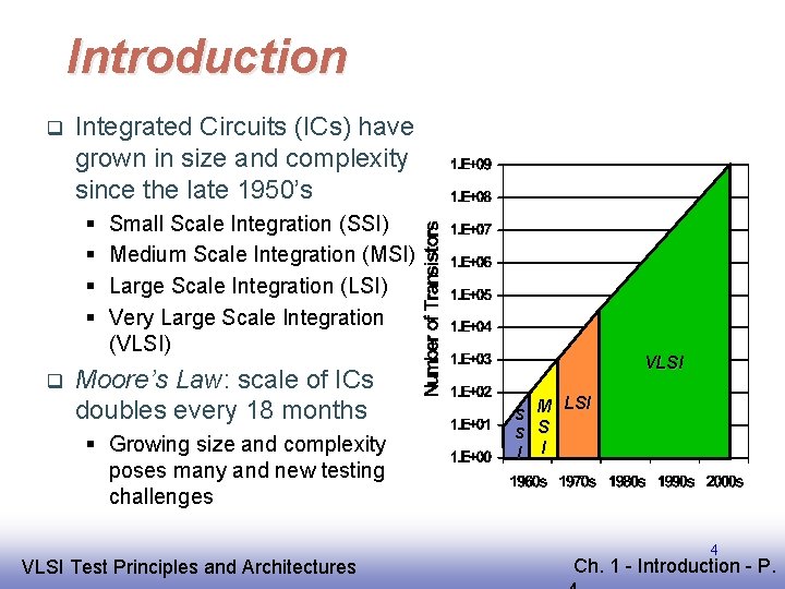
Introduction q Integrated Circuits (ICs) have grown in size and complexity since the late 1950’s § § q Small Scale Integration (SSI) Medium Scale Integration (MSI) Large Scale Integration (LSI) Very Large Scale Integration (VLSI) Moore’s Law: scale of ICs doubles every 18 months § Growing size and complexity poses many and new testing challenges EE 141 VLSI Test Principles and Architectures VLSI M LSI S S S I I 4 Ch. 1 - Introduction - P.

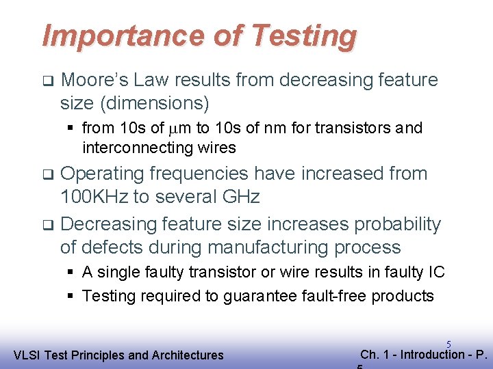
Importance of Testing q Moore’s Law results from decreasing feature size (dimensions) § from 10 s of m to 10 s of nm for transistors and interconnecting wires Operating frequencies have increased from 100 KHz to several GHz q Decreasing feature size increases probability of defects during manufacturing process q § A single faulty transistor or wire results in faulty IC § Testing required to guarantee fault-free products EE 141 VLSI Test Principles and Architectures 5 Ch. 1 - Introduction - P.

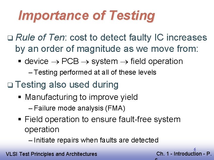
Importance of Testing q Rule of Ten: cost to detect faulty IC increases by an order of magnitude as we move from: § device PCB system field operation – Testing performed at all of these levels q Testing also used during § Manufacturing to improve yield – Failure mode analysis (FMA) § Field operation to ensure fault-free system operation – Initiate repairs when faults are detected EE 141 VLSI Test Principles and Architectures 6 Ch. 1 - Introduction - P.

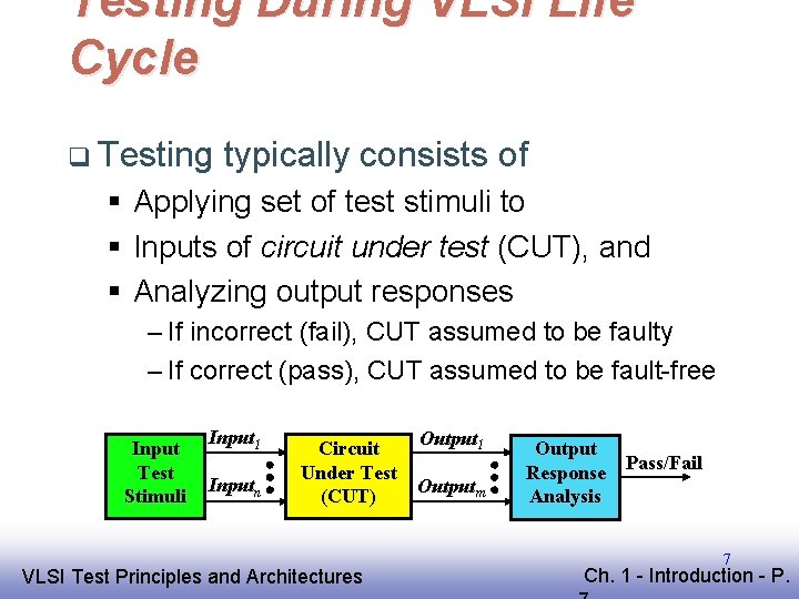
Testing During VLSI Life Cycle q Testing typically consists of § Applying set of test stimuli to § Inputs of circuit under test (CUT), and § Analyzing output responses – If incorrect (fail), CUT assumed to be faulty – If correct (pass), CUT assumed to be fault-free Input Test Stimuli Input 1 Inputn Circuit Under Test (CUT) EE 141 VLSI Test Principles and Architectures Output 1 Outputm Output Response Analysis Pass/Fail 7 Ch. 1 - Introduction - P.

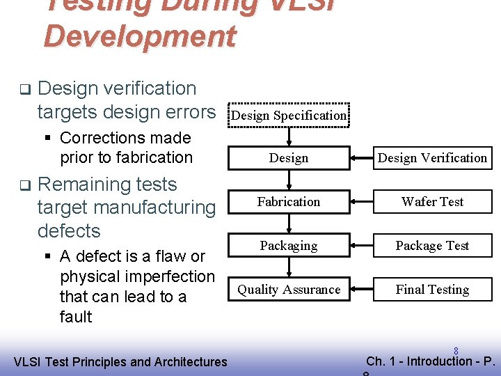
Testing During VLSI Development q Design verification targets design errors § Corrections made prior to fabrication q Design Specification Design Verification Remaining tests target manufacturing defects Fabrication Wafer Test § A defect is a flaw or physical imperfection that can lead to a fault Packaging Package Test Quality Assurance Final Testing EE 141 VLSI Test Principles and Architectures 8 Ch. 1 - Introduction - P.

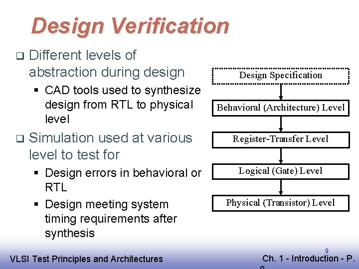
Design Verification q Different levels of abstraction during design § CAD tools used to synthesize design from RTL to physical level q Simulation used at various level to test for § Design errors in behavioral or RTL § Design meeting system timing requirements after synthesis EE 141 VLSI Test Principles and Architectures Design Specification Behavioral (Architecture) Level Register-Transfer Level Logical (Gate) Level Physical (Transistor) Level 9 Ch. 1 - Introduction - P.

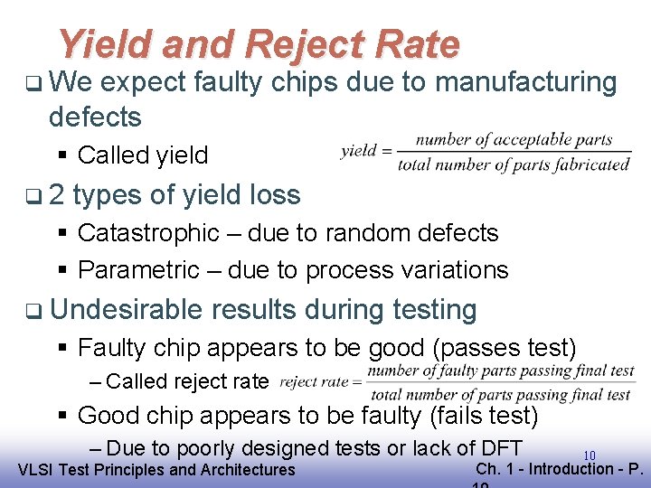
Yield and Reject Rate q We expect faulty chips due to manufacturing defects § Called yield q 2 types of yield loss § Catastrophic – due to random defects § Parametric – due to process variations q Undesirable results during testing § Faulty chip appears to be good (passes test) – Called reject rate § Good chip appears to be faulty (fails test) – Due to poorly designed tests or lack of DFT EE 141 VLSI Test Principles and Architectures 10 Ch. 1 - Introduction - P.

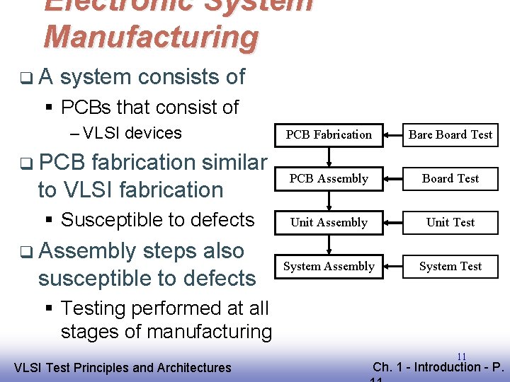
Electronic System Manufacturing q. A system consists of § PCBs that consist of – VLSI devices PCB Fabrication Bare Board Test fabrication similar to VLSI fabrication PCB Assembly Board Test § Susceptible to defects Unit Assembly Unit Test System Assembly System Test q PCB q Assembly steps also susceptible to defects § Testing performed at all stages of manufacturing EE 141 VLSI Test Principles and Architectures 11 Ch. 1 - Introduction - P.

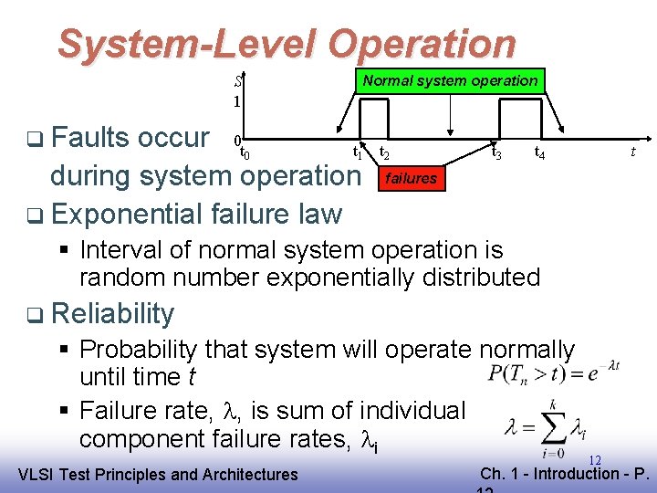
System-Level Operation S 1 q Faults Normal system operation occur 0 t t during system operation q Exponential failure law 0 1 t 2 t 3 t 4 t failures § Interval of normal system operation is random number exponentially distributed q Reliability § Probability that system will operate normally until time t § Failure rate, , is sum of individual component failure rates, i EE 141 VLSI Test Principles and Architectures 12 Ch. 1 - Introduction - P.

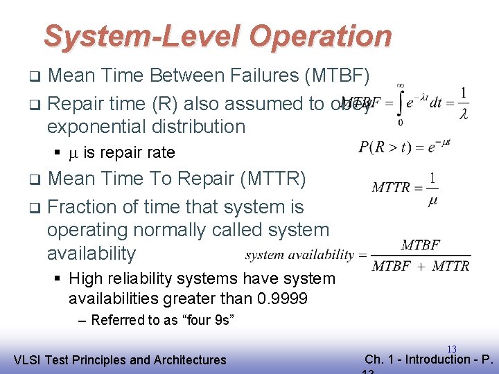
System-Level Operation Mean Time Between Failures (MTBF) q Repair time (R) also assumed to obey exponential distribution q § is repair rate Mean Time To Repair (MTTR) q Fraction of time that system is operating normally called system availability q § High reliability systems have system availabilities greater than 0. 9999 – Referred to as “four 9 s” EE 141 VLSI Test Principles and Architectures 13 Ch. 1 - Introduction - P.

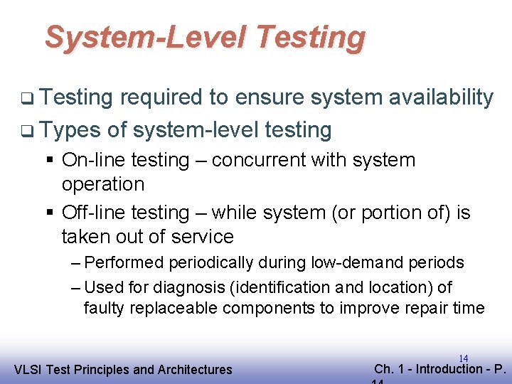
System-Level Testing q Testing required to ensure system availability q Types of system-level testing § On-line testing – concurrent with system operation § Off-line testing – while system (or portion of) is taken out of service – Performed periodically during low-demand periods – Used for diagnosis (identification and location) of faulty replaceable components to improve repair time EE 141 VLSI Test Principles and Architectures 14 Ch. 1 - Introduction - P.

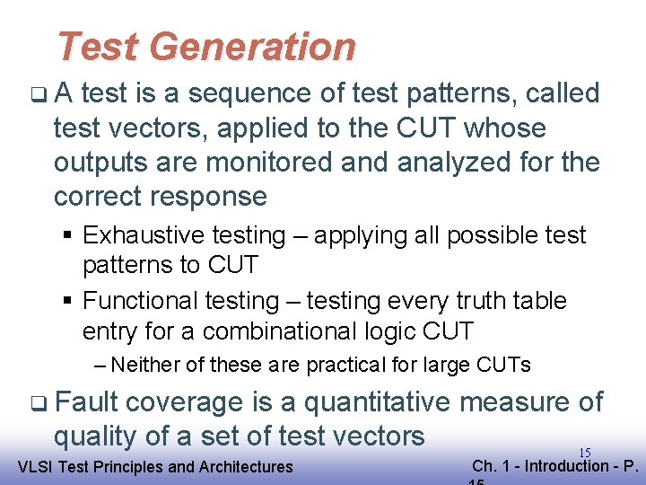
Test Generation q. A test is a sequence of test patterns, called test vectors, applied to the CUT whose outputs are monitored analyzed for the correct response § Exhaustive testing – applying all possible test patterns to CUT § Functional testing – testing every truth table entry for a combinational logic CUT – Neither of these are practical for large CUTs q Fault coverage is a quantitative measure of quality of a set of test vectors 15 EE 141 VLSI Test Principles and Architectures Ch. 1 - Introduction - P.

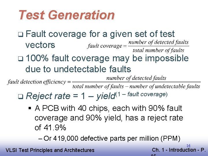
Test Generation q Fault coverage for a given set of test vectors q 100% fault coverage may be impossible due to undetectable faults q Reject rate = 1 – yield(1 – fault coverage) § A PCB with 40 chips, each with 90% fault coverage and 90% yield, has a reject rate of 41. 9% – Or 419, 000 defective parts per million (PPM) EE 141 VLSI Test Principles and Architectures 16 Ch. 1 - Introduction - P.

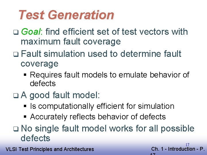
Test Generation q Goal: find efficient set of test vectors with maximum fault coverage q Fault simulation used to determine fault coverage § Requires fault models to emulate behavior of defects q. A good fault model: § Is computationally efficient for simulation § Accurately reflects behavior of defects q No single fault model works for all possible defects EE 141 VLSI Test Principles and Architectures 17 Ch. 1 - Introduction - P.

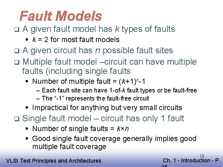
Fault Models q A given fault model has k types of faults § k = 2 for most fault models A given circuit has n possible fault sites q Multiple fault model –circuit can have multiple faults (including single faults q § Number of multiple fault = (k+1)n-1 – Each fault site can have 1 -of-k fault types or be fault-free – The “-1” represents the fault-free circuit § Impractical for anything but very small circuits q Single fault model – circuit has only 1 fault § Number of single faults = k×n § Good single fault coverage generally implies good multiple fault coverage EE 141 VLSI Test Principles and Architectures 18 Ch. 1 - Introduction - P.

Fault Models q Equivalent faults § One or more single faults that have identical behavior for all possible input patterns § Only one fault from a set of equivalent faults needs to be simulated q Fault collapsing § Removing equivalent faults – Except for one to be simulated § Reduces total number of faults – Reduces fault simulation time – Reduces test pattern generation time EE 141 VLSI Test Principles and Architectures 19 Ch. 1 - Introduction - P.

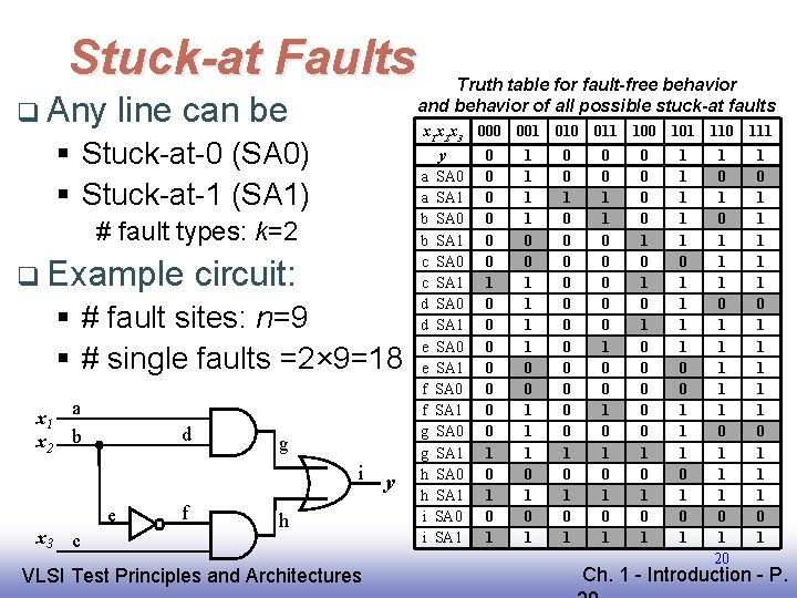
Stuck-at Faults q Any Truth table for fault-free behavior and behavior of all possible stuck-at faults line can be x 1 x 2 x 3 § Stuck-at-0 (SA 0) § Stuck-at-1 (SA 1) # fault types: k=2 q Example circuit: § # fault sites: n=9 § # single faults =2× 9=18 x 1 a x 2 b d g i x 3 c e f h EE 141 VLSI Test Principles and Architectures y a a b b c c d d e e f f g g h h i i y SA 0 SA 1 SA 0 SA 1 SA 0 SA 1 000 001 010 011 0 0 0 0 1 0 1 1 1 0 1 0 0 0 0 0 0 1 0 1 0 0 1 1 0 0 0 1 0 1 0 1 100 101 110 0 0 0 0 1 0 1 0 1 1 1 1 0 0 1 1 1 0 1 1 1 0 1 20 111 1 0 1 1 1 1 1 0 1 Ch. 1 - Introduction - P.

Stuck-at Faults q Valid Truth table for fault-free behavior and behavior of all possible stuck-at faults test vectors x 1 x 2 x 3 § Faulty circuit differs from good circuit § Necessary vectors: x 1 a x 2 b 011 detects f SA 1, e SA 0 100 detects d SA 1 – Detect total of 10 faults – 001 and 110 detect remaining 8 faults d g i x 3 c e f h EE 141 VLSI Test Principles and Architectures y a a b b c c d d e e f f g g h h i i y SA 0 SA 1 SA 0 SA 1 SA 0 SA 1 000 001 010 011 0 0 0 0 1 0 1 1 1 0 1 0 0 0 0 0 0 1 0 1 0 0 1 1 0 0 0 1 0 1 0 1 100 101 110 0 0 0 0 1 0 1 0 1 1 1 1 0 0 1 1 1 0 1 1 1 0 1 21 111 1 0 1 1 1 1 1 0 1 Ch. 1 - Introduction - P.

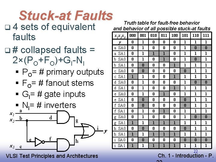
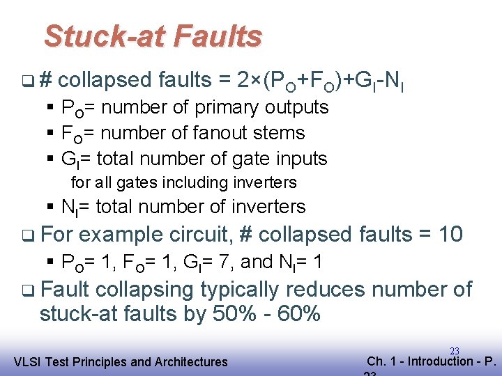
q 4 Stuck-at Faults Truth table for fault-free behavior and behavior of all possible stuck-at faults sets of equivalent faults q # collapsed faults = 2×(PO+FO)+GI-NI § § x 1 x 2 x 3 PO= # primary outputs FO= # fanout stems GI= # gate inputs NI= # inverters x 1 a x 2 b d g i x 3 c e f h EE 141 VLSI Test Principles and Architectures y a a b b c c d d e e f f g g h h i i y SA 0 SA 1 SA 0 SA 1 SA 0 SA 1 000 001 010 011 0 0 0 0 1 0 1 1 1 0 1 0 0 0 0 0 0 1 0 1 0 0 1 1 0 0 0 1 0 1 0 1 100 101 110 0 0 0 0 1 0 1 0 1 1 1 1 0 0 1 1 1 0 1 1 1 0 1 22 111 1 0 1 1 1 1 1 0 1 Ch. 1 - Introduction - P.

Stuck-at Faults q# collapsed faults = 2×(PO+FO)+GI-NI § PO= number of primary outputs § FO= number of fanout stems § GI= total number of gate inputs for all gates including inverters § NI= total number of inverters q For example circuit, # collapsed faults = 10 § PO= 1, FO= 1, GI= 7, and NI= 1 q Fault collapsing typically reduces number of stuck-at faults by 50% - 60% EE 141 VLSI Test Principles and Architectures 23 Ch. 1 - Introduction - P.

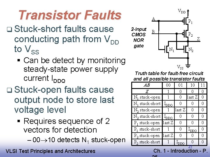
VDD Transistor Faults q Any transistor can be § Stuck-short – Also known as stuck-short § Stuck-open – Also known as stuck-open # fault types: k=2 q Example circuit § # fault sites: n=4 § # single faults =2× 4=8 EE 141 VLSI Test Principles and Architectures A 2 -input CMOS NOR gate P 1 B P 2 N 1 Z N 2 VSS Truth table for fault-free circuit and all possible transistor faults AB 00 01 10 11 Z 1 0 0 0 N 1 stuck-open 1 0 last Z 0 N 1 stuck-short IDDQ 0 0 0 N 2 stuck-open 1 last Z 0 0 N 2 stuck-short IDDQ 0 0 0 P 1 stuck-open last Z 0 0 0 P 1 stuck-short 1 0 IDDQ 0 P 2 stuck-open last Z 0 0 0 P 2 stuck-short 1 IDDQ 0 0 24 Ch. 1 - Introduction - P.

VDD Transistor Faults q Stuck-short faults cause conducting path from VDD to VSS § Can be detect by monitoring steady-state power supply current IDDQ q Stuck-open faults cause output node to store last voltage level § Requires sequence of 2 vectors for detection – 00 10 detects N 1 stuck-open EE 141 VLSI Test Principles and Architectures A 2 -input CMOS NOR gate P 1 B P 2 N 1 Z N 2 VSS Truth table for fault-free circuit and all possible transistor faults AB 00 01 10 11 Z 1 0 0 0 N 1 stuck-open 1 0 last Z 0 N 1 stuck-short IDDQ 0 0 0 N 2 stuck-open 1 last Z 0 0 N 2 stuck-short IDDQ 0 0 0 P 1 stuck-open last Z 0 0 0 P 1 stuck-short 1 0 IDDQ 0 P 2 stuck-open last Z 0 0 0 P 2 stuck-short 1 IDDQ 0 0 25 Ch. 1 - Introduction - P.

Transistor Faults q# § § § collapsed faults = 2×T -TS+GS -TP+GP T = number of transistors TS= number of series transistors GS= number of groups of series transistors TP= number of parallel transistors GP= number of groups of parallel transistors q For example circuit, # collapsed faults = 6 § T=4, TS= 2, GS= 1, TP= 2, & GP= 1 q Fault collapsing typically reduces number of transistor faults by 25% to 35% EE 141 VLSI Test Principles and Architectures 26 Ch. 1 - Introduction - P.

Shorts and Opens q Wires can be § Open – Opens in wires interconnecting transistors to form gates behave like transistor stuck-open faults – Opens in wires interconnecting gates to form circuit behave like stuck-at faults – Opens are detected by vectors detecting transistor and stuck-at faults § Short to an adjacent wire – Also known as a bridging fault EE 141 VLSI Test Principles and Architectures 27 Ch. 1 - Introduction - P.

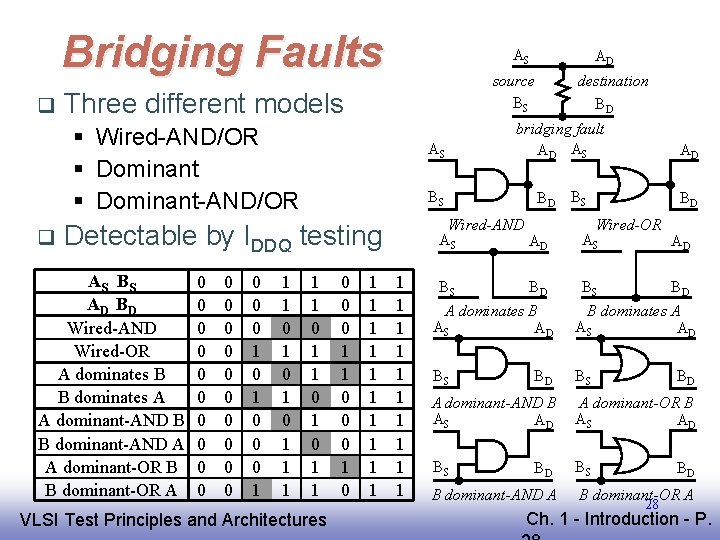
Bridging Faults q AS source BS Three different models § Wired-AND/OR § Dominant-AND/OR q Detectable by IDDQ testing AS B S AD B D Wired-AND Wired-OR A dominates B B dominates A A dominant-AND B B dominant-AND A A dominant-OR B B dominant-OR A 0 0 0 0 0 0 1 0 0 0 1 1 1 0 1 0 1 1 EE 141 VLSI Test Principles and Architectures 0 0 0 1 1 1 1 1 1 AD 1 1 1 1 1 destination BD AS bridging fault AD AS AD BS BD Wired-AND AS AD BS BS BD BD Wired-OR A dominates B AS AD B dominates A AS AD BS BS BD BD A dominant-AND B AS AD A dominant-OR B AS AD BS BS BD B dominant-AND A BD B dominant-OR A 28 Ch. 1 - Introduction - P.

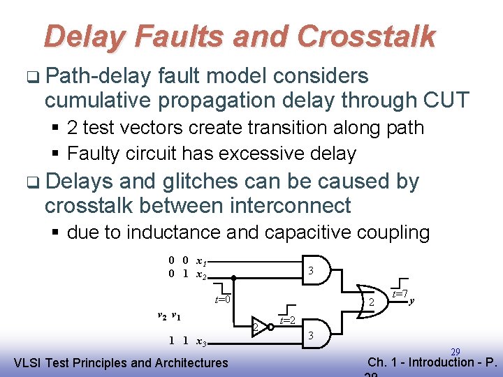
Delay Faults and Crosstalk q Path-delay fault model considers cumulative propagation delay through CUT § 2 test vectors create transition along path § Faulty circuit has excessive delay q Delays and glitches can be caused by crosstalk between interconnect § due to inductance and capacitive coupling 0 0 x 1 0 1 x 2 3 t=0 v 2 v 1 1 1 x 3 EE 141 VLSI Test Principles and Architectures 2 2 t=7 y t=2 3 29 Ch. 1 - Introduction - P.

Pattern Sensitivity and Coupling Faults q Common in high density RAMs q Pattern sensitivity fault § Contents of memory cell is affected by contents of neighboring cells q Coupling fault § Transition in contents of one memory cell causes change in contents of another cell EE 141 VLSI Test Principles and Architectures 30 Ch. 1 - Introduction - P.

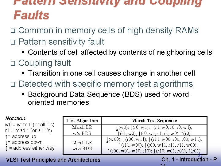
Pattern Sensitivity and Coupling Faults Common in memory cells of high density RAMs q Pattern sensitivity fault q § Contents of cell affected by contents of neighboring cells q Coupling fault § Transition in one cell causes change in another cell q Detected with specific memory test algorithms § Background Data Sequence (BDS) used for wordoriented memories Notation: w 0 = write 0 (or all 0’s) r 1 = read 1 (or all 1’s) ↑= address up ↓= address down ↨ = address either way Test Algorithm March LR w/o BDS March LR with BDS EE 141 VLSI Test Principles and Architectures March Test Sequence ↨(w 0); ↓(r 0, w 1); ↑(r 1, w 0, r 0, w 1); ↑(r 1, w 0); ↑(r 0, w 1, r 1, w 0); ↑(r 0) ↨(w 00); ↓(r 00, w 11); ↑(r 11, w 00, r 00, w 11); ↑(r 11, w 00); ↑(r 00, w 11, r 11, w 00); ↑(r 00, w 01, w 10, r 10); ↑(r 10, w 01, r 01); ↑(r 01) 31 Ch. 1 - Introduction - P.

Analog Fault Models q Catastrophic faults § Shorts and opens q Parametric faults § Parametric variations in passive and active components cause components to be out of tolerance range q Active components can sustain defects that affect DC and/or AC operation EE 141 VLSI Test Principles and Architectures 32 Ch. 1 - Introduction - P.

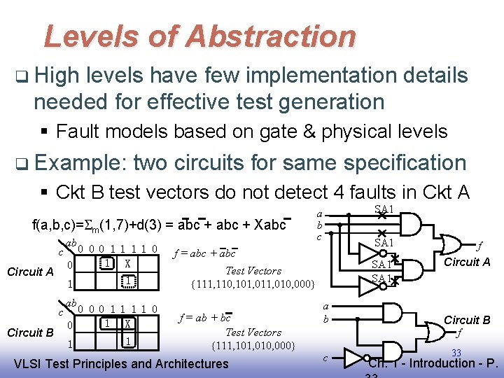
Levels of Abstraction q High levels have few implementation details needed for effective test generation § Fault models based on gate & physical levels q Example: two circuits for same specification § Ckt B test vectors do not detect 4 faults in Ckt A f(a, b, c)= m(1, 7)+d(3) = abc + Xabc ab c 0 00 11 11 0 1 X 0 Circuit A 1 1 c Circuit B SA 1 f = abc + abc SA 1 Test Vectors {111, 110, 101, 010, 000} ab 0 00 11 11 0 1 X 0 1 1 SA 1 a b c f = ab + bc Test Vectors {111, 101, 010, 000} EE 141 VLSI Test Principles and Architectures a b c f Circuit A Circuit B f 33 Ch. 1 - Introduction - P.

Overview of VLSI Test Technology q Automatic Test Equipment (ATE) consists of § Computer – for central control and flexible test & measurement for different products § Pin electronics & fixtures – to apply test patterns to pins & sample responses § Test program – controls timing of test patterns & compares response to known good responses EE 141 VLSI Test Principles and Architectures 34 Ch. 1 - Introduction - P.

Overview of VLSI Test Technology q Automatic Test Pattern Generation (ATPG) § Algorithms generating sequence of test vectors for a given circuit based on specific fault models q Fault simulation § Emulates fault models in CUT and applies test vectors to determine fault coverage § Simulation time (significant due to large number of faults to emulate) can be reduced by – Parallel, deductive, and concurrent fault simulation EE 141 VLSI Test Principles and Architectures 35 Ch. 1 - Introduction - P.

Overview of VLSI Test Technology q Design for Testability (DFT) § Generally incorporated in design § Goal: improve controllability and/or observability of internal nodes of a chip or PCB q Three basic approaches § Ad-hoc techniques § Scan design – Boundary Scan § Built-In Self-Test (BIST) EE 141 VLSI Test Principles and Architectures 36 Ch. 1 - Introduction - P.

Design of Testability q Ad-hoc DFT techniques § Add internal test points (usually multiplexers) for – Controllability – Observability § Added on a case-by-case basis – Primarily targets “hard to test” portions of chip Normal system data Test data input Test mode select 0 1 Internal node to be controlled controllability test point EE 141 VLSI Test Principles and Architectures Normal system data Internal node to be observed Test mode select 0 1 Primary output observability test point 37 Ch. 1 - Introduction - P.

Design for Testability Primary q Scan § Transforms flip-flops of chip into a shift register § Scan mode facilitates – Shifting in test vectors – Shifting out responses q Good Inputs design CAD tool support § Transforming flip-flops to shift register § ATPG EE 141 VLSI Test Principles and Architectures Primary Combinational Outputs Logic FFs 1 Di Clk FF Qi 2 Di 0 1 Qi-1 Scan Clk Mode FF Qi 3 Primary Combinational Outputs Inputs Logic Scan Data Out FFs 38 Scan Data In Ch. 1 - Introduction - P.

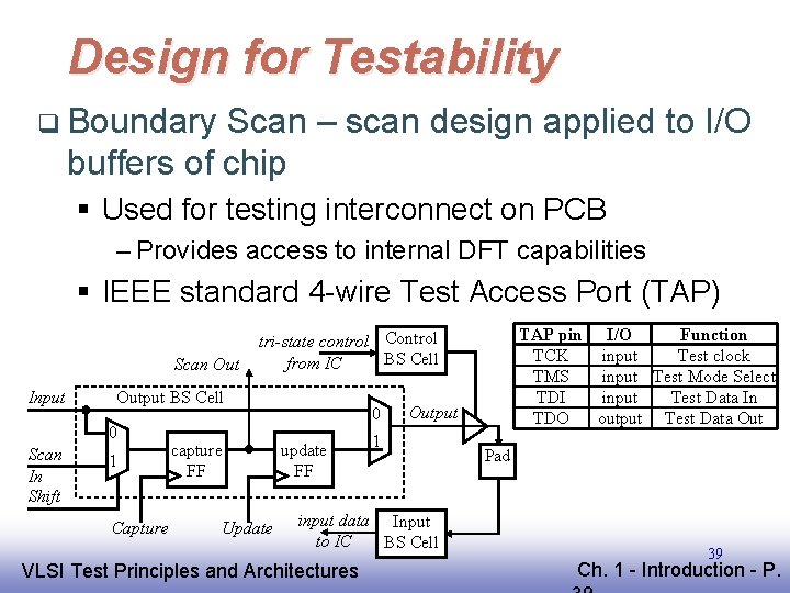
Design for Testability q Boundary Scan – scan design applied to I/O buffers of chip § Used for testing interconnect on PCB – Provides access to internal DFT capabilities § IEEE standard 4 -wire Test Access Port (TAP) Scan Out Input Output BS Cell 0 Scan In Shift 1 Capture TAP pin I/O Function TCK input Test clock TMS input Test Mode Select TDI input Test Data In TDO output Test Data Out tri-state control Control BS Cell from IC capture FF Update 0 update FF Output 1 input data Input to IC BS Cell EE 141 VLSI Test Principles and Architectures Pad 39 Ch. 1 - Introduction - P.

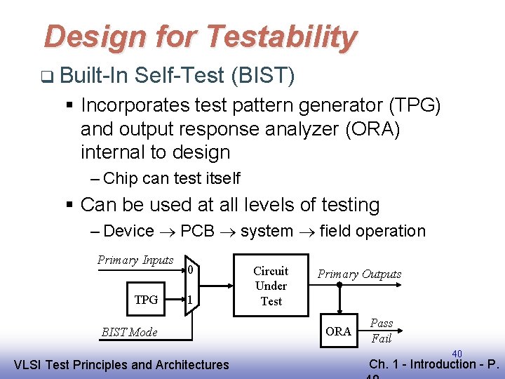
Design for Testability q Built-In Self-Test (BIST) § Incorporates test pattern generator (TPG) and output response analyzer (ORA) internal to design – Chip can test itself § Can be used at all levels of testing – Device PCB system field operation Primary Inputs TPG 0 1 BIST Mode EE 141 VLSI Test Principles and Architectures Circuit Under Test Primary Outputs ORA Pass Fail 40 Ch. 1 - Introduction - P.

Concluding Remarks q Many new testing challenges presented by § Increasing size and complexity of VLSI devices § Decreasing feature size q This chapter presented introduction to VLSI testing q Remaining chapters present more details as well as solutions to these challenges EE 141 VLSI Test Principles and Architectures 41 Ch. 1 - Introduction - P.