Chapter 05 Tutorial Using HDL Based Design Verilog

Chapter 05 Tutorial Using HDL Based Design Verilog Language
Objective n n n This tutorial will give you exposure to using HDL based design Using Verilog and Modelsim for simulating the functional design This tutorial shows you how to create, using Verilog, a simple combinational logic circuit design
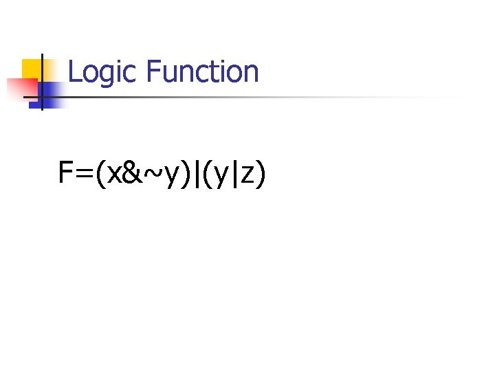
Logic Function F=(x&~y)|(y|z)
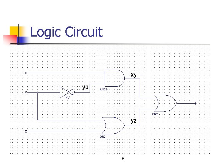
Logic Circuit 6

Implementation Methods n n Method 1: Using the automatic module generator Method 2: Using the user free input
Method 1 n Using the automatic module generator

Create a New Project

Enter a Name and Location for the Project

Select the Device and Design Flow for the Project

Create a New Source

Select Verilog Module and Enter File Name

Define Verilog Source

New Source Information

Finish

Next Step

Input Logic Function

Add Test Bench Source

Add Test Bench Waveform

Select Source File

New Source Information
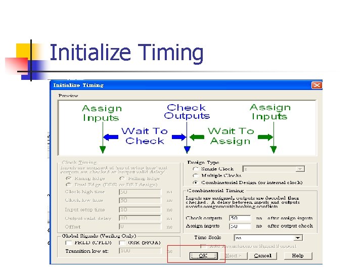
Initialize Timing

Waveform Created by HDL Bencher

Save the Waveform

View Behavioral Text Fixture

Simulate Behavioral Model
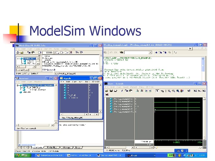
Model. Sim Windows

Wave Window

Verifying the Logic Function F=(x & ~y)|(y|z)

Question and Answer

Method 2 n Using the user free input
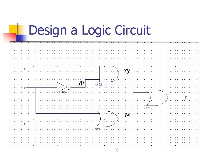
Design a Logic Circuit 6

Create a New Project 2

Enter a Name and Location for the Project 3

Create a New File 4

Free Input Verilog Language in the New File 5
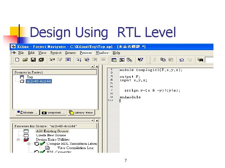
Design Using RTL Level 7

Design Using Gate Level 8

Save the Design 9
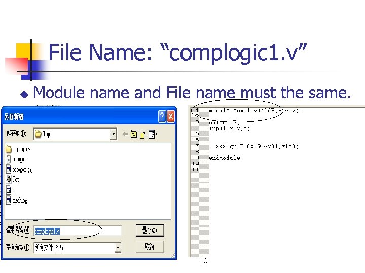
File Name: “complogic 1. v” u Module name and File name must the same. 10

Add Source into the Project 11

Select “complogic 1. v” 12
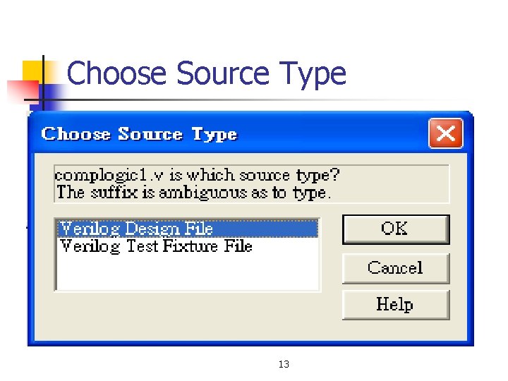
Choose Source Type 13

Add New Source for Test Bench Waveform 14

Select Test Bench Waveform 15
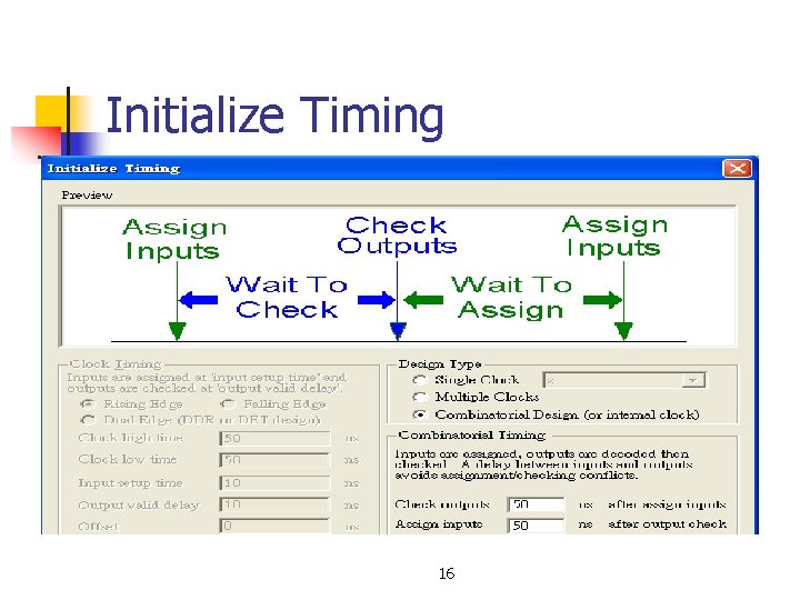
Initialize Timing 16

Waveform Created by HDL Bencher 17
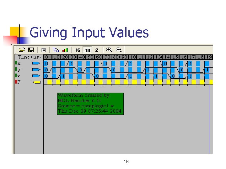
Giving Input Values 18

Save the Waveform 19

Select “View Behavioral. . ” and Run 20

See a HDL Test bench 21

Select “Generate Expected. . ” and Run 22
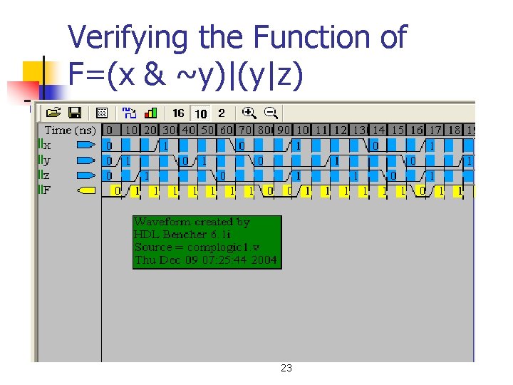
Verifying the Function of F=(x & ~y)|(y|z) 23

Question & Answer
- Slides: 53