Chapter 03 ModuleBased Digital Circuit Design and Verification

Chapter 03 Module-Based Digital Circuit Design and Verification 1
 24")
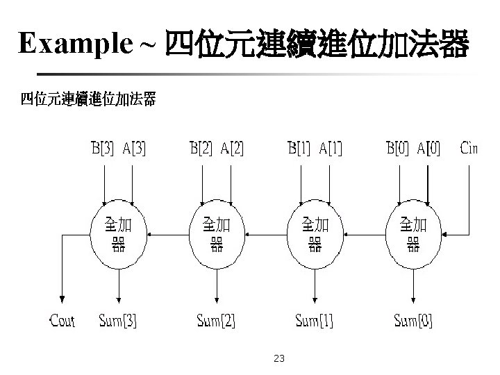
Example (cont. ) 24

Create New Schematic v Select “New Source” and type “ser_adder” under the File name. 25
 v See “ser_adder” in the project and you can")
Create New Schematic (cont. ) v See “ser_adder” in the project and you can use “full_adder” in the symbols. 26
 v Select “full_adder” symbol. 27")
Example (cont. ) v Select “full_adder” symbol. 27
 v To complete circuit. 28")
Example (cont. ) v To complete circuit. 28
 v To check and “Save”. 29")
Example (cont. ) v To check and “Save”. 29
 v You can see the schematic hierarchy and start to simulation,")
Example (cont. ) v You can see the schematic hierarchy and start to simulation, so select “New Source” to add test bench wave. 30
 v Type “test_ser_adder” under the File name and give “input” to")
Example (cont. ) v Type “test_ser_adder” under the File name and give “input” to the circuit and “Save”. 31
 v Select “View Behavioral Test…” and you can see test bench.")
Example (cont. ) v Select “View Behavioral Test…” and you can see test bench. 32
 v Select “Simulate Behavioral Model” and Run. 33")
Example (cont. ) v Select “Simulate Behavioral Model” and Run. 33
 v You can see “loading error”, so need to add source.")
Example (cont. ) v You can see “loading error”, so need to add source. 34
 v Select View Source and select File Open. 35")
Example (cont. ) v Select View Source and select File Open. 35
 v To “src” choose symbols that we need. 36")
Example (cont. ) v To “src” choose symbols that we need. 36
 v Select AND 2, OR 3, XOR 3 and Select compile.")
Example (cont. ) v Select AND 2, OR 3, XOR 3 and Select compile. 37
 38")
Example (cont. ) 38
 v Double-Click “test_ser_adder” and you can see “sim” and select “Add")
Example (cont. ) v Double-Click “test_ser_adder” and you can see “sim” and select “Add to Wave”. 39
 v Select Run-all or Continue Run. 40")
Example (cont. ) v Select Run-all or Continue Run. 40
 v Result. 41")
Example (cont. ) v Result. 41
- Slides: 20