Chap 5 2 Silicon and wafer preparation 4

- Slides: 15

Chap 5 -2. Silicon and wafer preparation

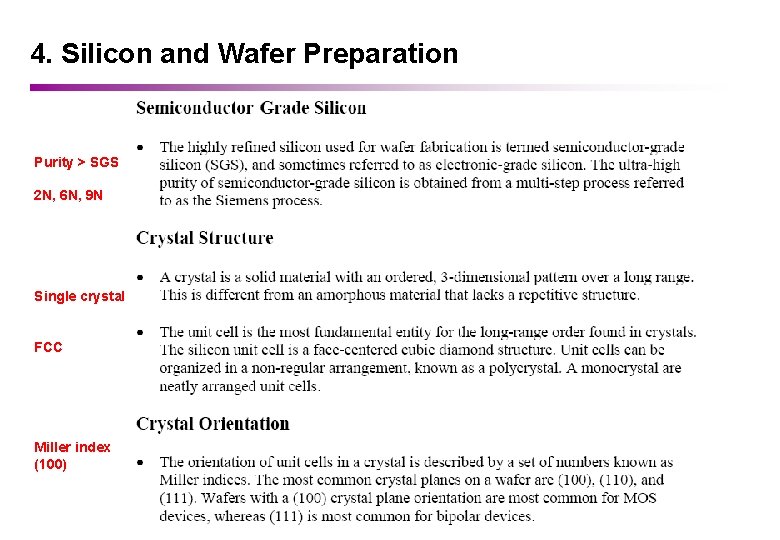
4. Silicon and Wafer Preparation Purity > SGS 2 N, 6 N, 9 N Single crystal FCC Miller index (100)

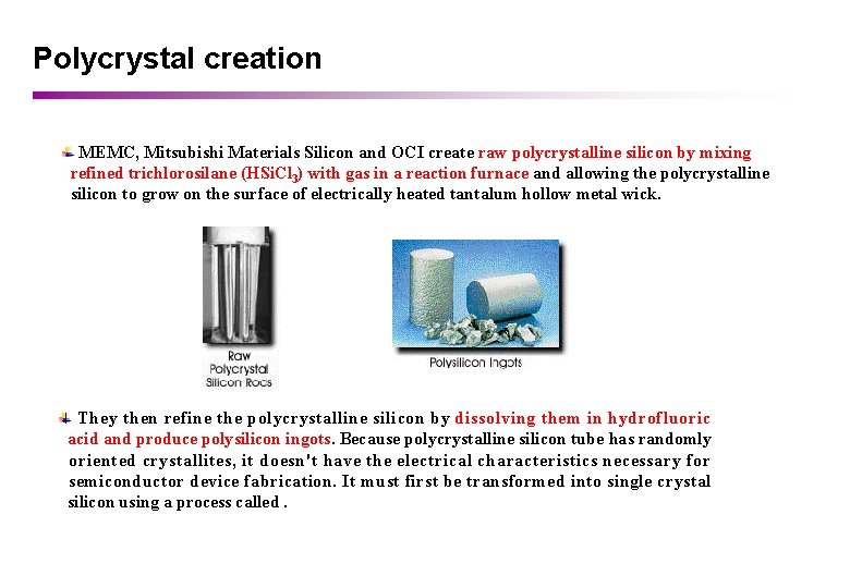
Polycrystal creation MEMC, Mitsubishi Materials Silicon and OCI create raw polycrystalline silicon by mixing refined trichlorosilane (HSi. Cl 3) with gas in a reaction furnace and allowing the polycrystalline silicon to grow on the surface of electrically heated tantalum hollow metal wick. They then refine the polycrystalline silicon by dissolving them in hydrofluoric acid and produce polysilicon ingots. Because polycrystalline silicon tube has randomly oriented crystallites, it doesn't have the electrical characteristics necessary for semiconductor device fabrication. It must first be transformed into single crystal silicon using a process called.

4. Silicon and Wafer Preparation

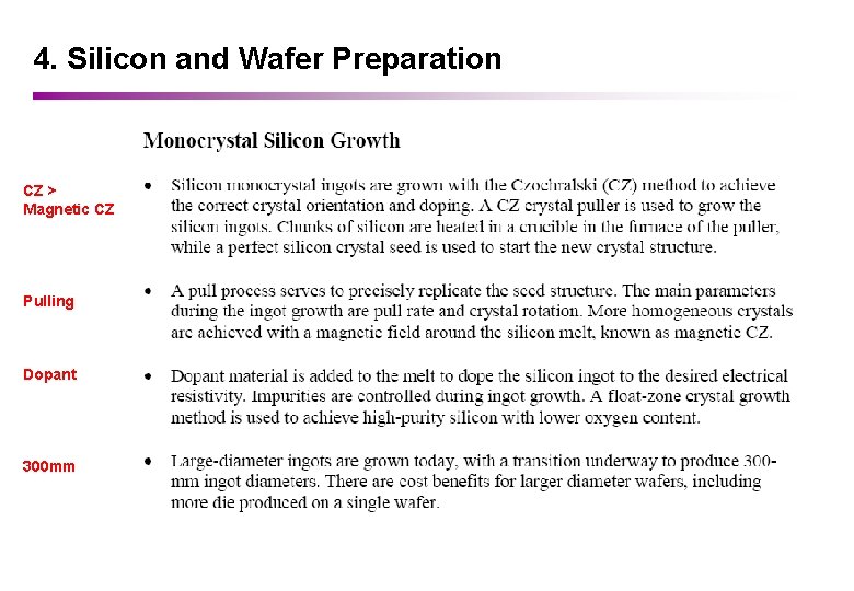
4. Silicon and Wafer Preparation CZ > Magnetic CZ Pulling Dopant 300 mm

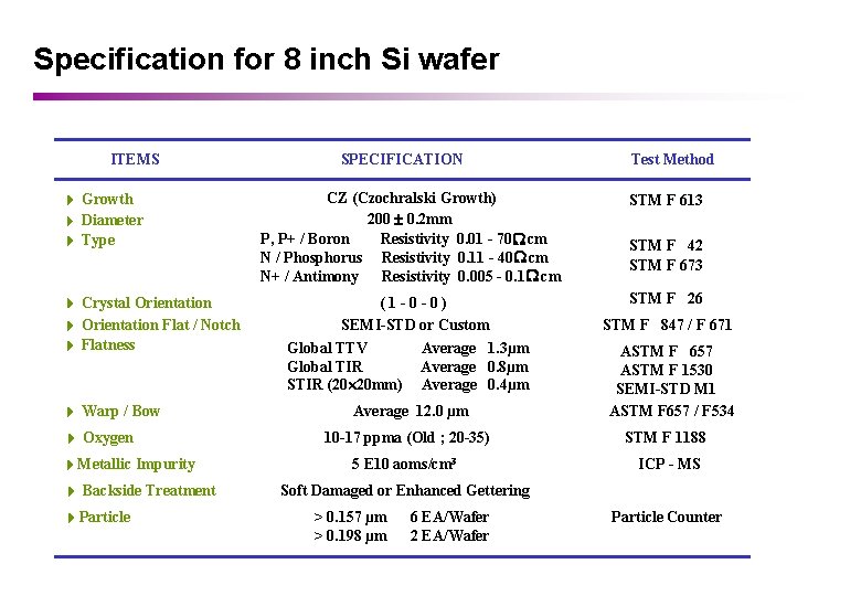
Specification for 8 inch Si wafer ITEMS Growth Diameter Type Crystal Orientation Flat / Notch Flatness Warp / Bow Oxygen Metallic Impurity Backside Treatment Particle SPECIFICATION Test Method CZ (Czochralski Growth) 200 0. 2 mm P, P+ / Boron Resistivity 0. 01 - 70 cm N / Phosphorus Resistivity 0. 11 - 40 cm N+ / Antimony Resistivity 0. 005 - 0. 1 cm STM F 613 (1 -0 -0) SEMI-STD or Custom Global TTV Average 1. 3µm Global TIR Average 0. 8µm STIR (20 20 mm) Average 0. 4µm STM F 26 Average 12. 0 µm STM F 42 STM F 673 STM F 847 / F 671 ASTM F 657 ASTM F 1530 SEMI-STD M 1 ASTM F 657 / F 534 10 -17 ppma (Old ; 20 -35) STM F 1188 5 E 10 aoms/cm 3 ICP - MS Soft Damaged or Enhanced Gettering > 0. 157 µm > 0. 198 µm 6 EA/Wafer 2 EA/Wafer Particle Counter

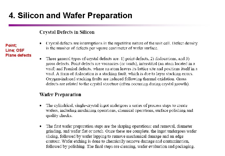
4. Silicon and Wafer Preparation Point; Line; OSF Plane defects

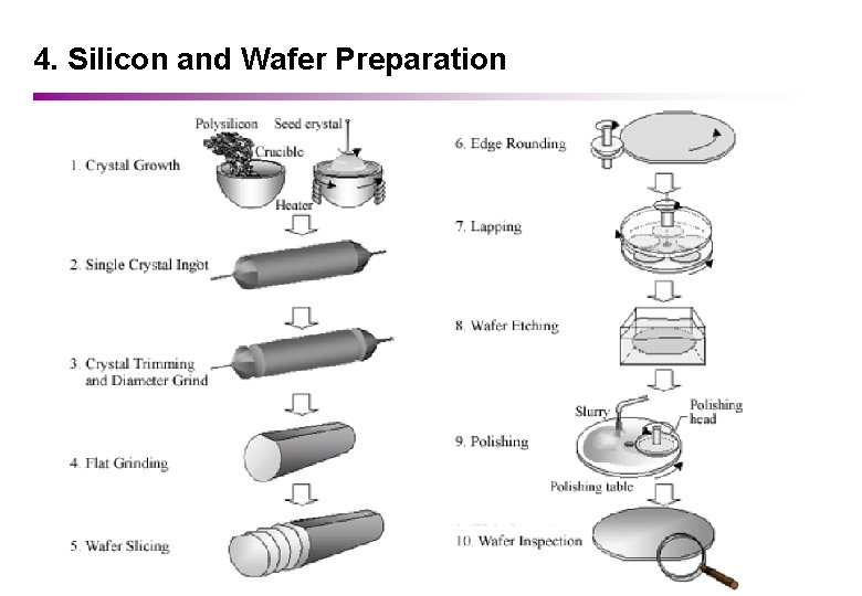
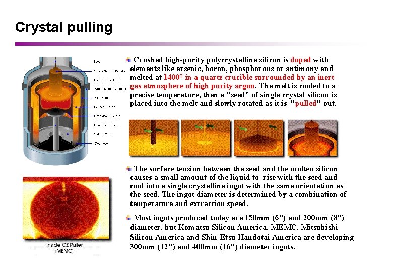
Crystal pulling Crushed high-purity polycrystalline silicon is doped with elements like arsenic, boron, phosphorous or antimony and melted at 1400° in a quartz crucible surrounded by an inert gas atmosphere of high purity argon. The melt is cooled to a precise temperature, then a "seed” of single crystal silicon is placed into the melt and slowly rotated as it is "pulled" out. The surface tension between the seed and the molten silicon causes a small amount of the liquid to rise with the seed and cool into a single crystalline ingot with the same orientation as the seed. The ingot diameter is determined by a combination of temperature and extraction speed. Most ingots produced today are 150 mm (6") and 200 mm (8") diameter, but Komatsu Silicon America, MEMC, Mitsubishi Silicon America and Shin-Etsu Handotai America are developing 300 mm (12") and 400 mm (16") diameter ingots.

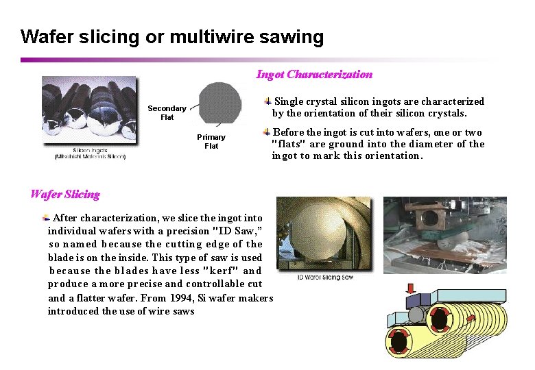
Wafer slicing or multiwire sawing Ingot Characterization Single crystal silicon ingots are characterized by the orientation of their silicon crystals. Secondary Flat Primary Flat Before the ingot is cut into wafers, one or two "flats" are ground into the diameter of the ingot to mark this orientation. Wafer Slicing After characterization, we slice the ingot into individual wafers with a precision "ID Saw, ” so named because the cutting edge of the blade is on the inside. This type of saw is used because the blades have less "kerf" and produce a more precise and controllable cut and a flatter wafer. From 1994, Si wafer makers introduced the use of wire saws

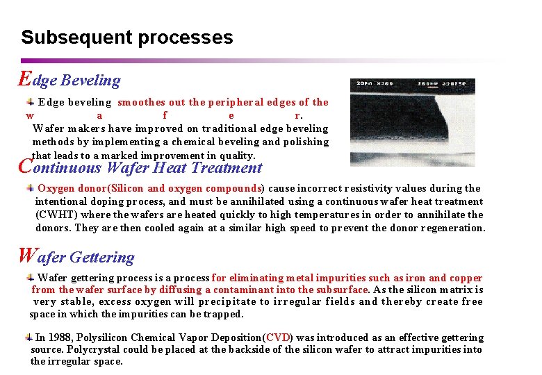
Subsequent processes Edge Beveling Edge beveling smoothes out the peripheral edges of the w a f e r. Wafer makers have improved on traditional edge beveling methods by implementing a chemical beveling and polishing that leads to a marked improvement in quality. Continuous Wafer Heat Treatment Oxygen donor(Silicon and oxygen compounds) cause incorrect resistivity values during the intentional doping process, and must be annihilated using a continuous wafer heat treatment (CWHT) where the wafers are heated quickly to high temperatures in order to annihilate the donors. They are then cooled again at a similar high speed to prevent the donor regeneration. Wafer Gettering Wafer gettering process is a process for eliminating metal impurities such as iron and copper from the wafer surface by diffusing a contaminant into the subsurface. As the silicon matrix is very stable, excess oxygen will precipitate to irregular fields and thereby create free space in which the impurities can be trapped. In 1988, Polysilicon Chemical Vapor Deposition(CVD) was introduced as an effective gettering source. Polycrystal could be placed at the backside of the silicon wafer to attract impurities into the irregular space.

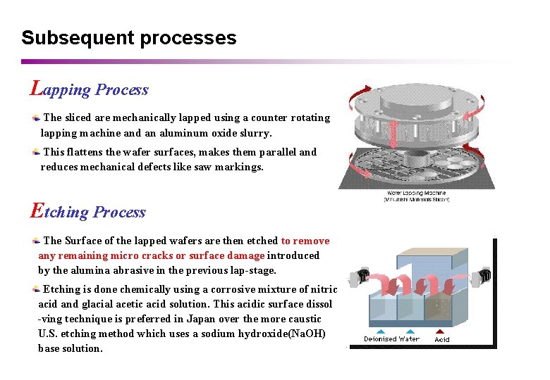
Subsequent processes Lapping Process The sliced are mechanically lapped using a counter rotating lapping machine and an aluminum oxide slurry. This flattens the wafer surfaces, makes them parallel and reduces mechanical defects like saw markings. Etching Process The Surface of the lapped wafers are then etched to remove any remaining micro cracks or surface damage introduced by the alumina abrasive in the previous lap-stage. Etching is done chemically using a corrosive mixture of nitric acid and glacial acetic acid solution. This acidic surface dissol -ving technique is preferred in Japan over the more caustic U. S. etching method which uses a sodium hydroxide(Na. OH) base solution.

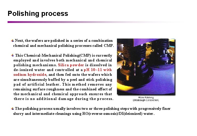
Polishing process Next, the wafers are polished in a series of a combination chemical and mechanical polishing processes called CMP. This Chemical-Mechanical Polishing(CMP) is currently employed and involves both mechanical and chemical polishing mechanisms. Silica powder is dissolved in de-ionized water and controlled at a p. H 10~11 with sodium hydroxide, and then fed onto the wafers which are simultaneously buffed by a peel and stick polishing pad of artificial leather. This method removes any remaining surface roughness and the combined effect of the mechanical and chemical approach ensures that there is no additional damage during the process. The polishing process usually involves two or three polishing steps with progressively finer slurry and intermediate cleanings using RO(reverse osmosis)/DI(deionized) water.

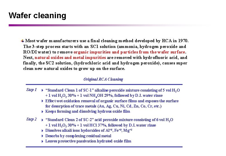
Wafer cleaning Most wafer manufacturers use a final cleaning method developed by RCA in 1970. The 3 -step process starts with an SC 1 solution (ammonia, hydrogen peroxide and RO/DI water) to remove organic impurities and particles from the wafer surface. Next, natural oxides and metal impurities are removed with hydrofluoric acid, and finally, the SC 2 solution, (hydrochloric acid and hydrogen peroxide), causes super clean new natural oxides to grow up on the surface. Original RCA Cleaning Step 1 “Standard Clean 1 of SC-1” alkaline peroxide mixture consisting of 5 vol H 2 O + 1 vol H 2 O 2 30% + 1 vol NH 4 OH 29%, followed by D. I. water rinse Effect wet oxidation removal of organic surface films and exposes the surface for desorption of trace metals (Au, Ag, Cu, Ni, Cd, Zn, Co, Cr, etc. ) Keeps forming and dissolving hydrous oxide film Step 2 “Standard Clean 2 of SC-2” acid peroxide mixture consisting of 6 vol H 2 O + 1 vol H 2 O 2 30% + 1 vol HCl 37%, followed by D. I. water rinse Dissolves alkali ions hydorxides of Al+3, Fe+3, Mg+2 Desorbs by complexing residual metal Leaves protective passivation hydrated oxide film

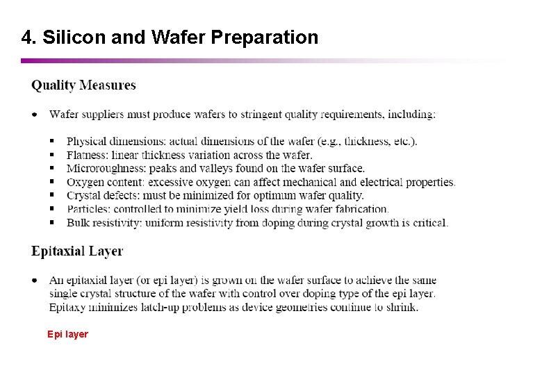
4. Silicon and Wafer Preparation Epi layer

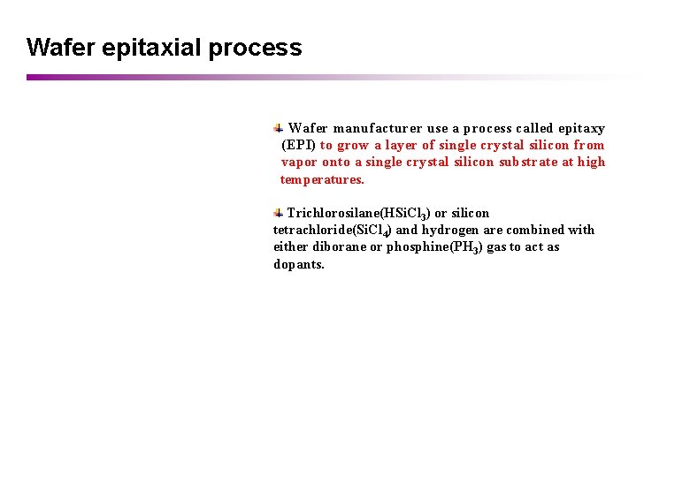
Wafer epitaxial process Wafer manufacturer use a process called epitaxy (EPI) to grow a layer of single crystal silicon from vapor onto a single crystal silicon substrate at high temperatures. Trichlorosilane(HSi. Cl 3) or silicon tetrachloride(Si. Cl 4) and hydrogen are combined with either diborane or phosphine(PH 3) gas to act as dopants.