Channel Control ASIC for the CMS Hadron Calorimeter
- Slides: 23

Channel Control ASIC for the CMS Hadron Calorimeter Front End Readout Module Ray Yarema, Alan Baumbaugh, Ahmed Boubekeur, John Elias, Theresa Shaw September 12, 2002 September 8 -14, 2002 7 th Workshop on Electronics for LHC 1

CCA Use in CMS • CCAs are used for processing both HPD and PMT signals • CCA provides control and interface for QIE ASICs which digitize charge input signals. • CCAs and QIEs are mounted on the CMS Hadron Calorimeter Front End Readout Module • CCAs and QIEs were designed at Fermilab September 8 -14, 2002 7 th Workshop on Electronics for LHC 2

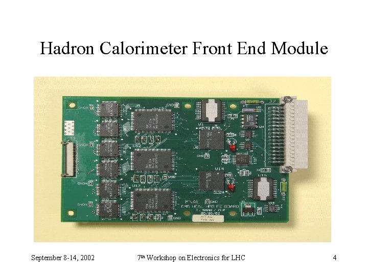
Front End Readout Module • Two QIE chips interface to one CCA chip • There are 3 CCA chips on a Front End Readout Module • 3 CCAs feed data to 2 GOLs September 8 -14, 2002 7 th Workshop on Electronics for LHC 3

Hadron Calorimeter Front End Module September 8 -14, 2002 7 th Workshop on Electronics for LHC 4

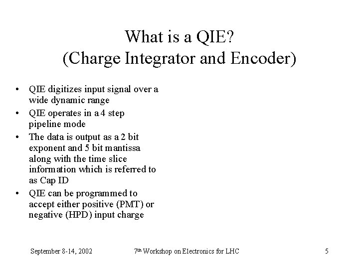
What is a QIE? (Charge Integrator and Encoder) • QIE digitizes input signal over a wide dynamic range • QIE operates in a 4 step pipeline mode • The data is output as a 2 bit exponent and 5 bit mantissa along with the time slice information which is referred to as Cap ID • QIE can be programmed to accept either positive (PMT) or negative (HPD) input charge September 8 -14, 2002 7 th Workshop on Electronics for LHC 5

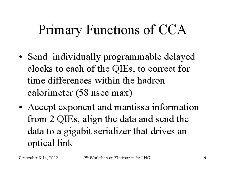
Primary Functions of CCA • Send individually programmable delayed clocks to each of the QIEs, to correct for time differences within the hadron calorimeter (58 nsec max) • Accept exponent and mantissa information from 2 QIEs, align the data and send the data to a gigabit serializer that drives an optical link September 8 -14, 2002 7 th Workshop on Electronics for LHC 6

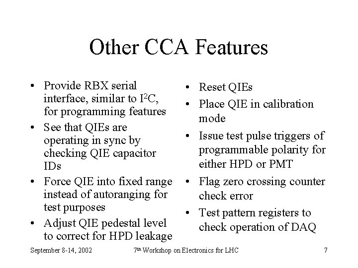
Other CCA Features • Provide RBX serial interface, similar to I 2 C, for programming features • See that QIEs are operating in sync by checking QIE capacitor IDs • Force QIE into fixed range instead of autoranging for test purposes • Adjust QIE pedestal level to correct for HPD leakage September 8 -14, 2002 • Reset QIEs • Place QIE in calibration mode • Issue test pulse triggers of programmable polarity for either HPD or PMT • Flag zero crossing counter check error • Test pattern registers to check operation of DAQ 7 th Workshop on Electronics for LHC 7

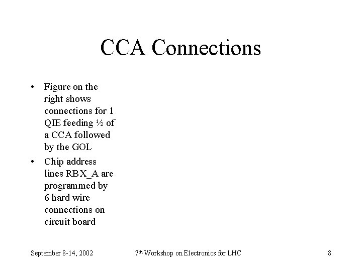
CCA Connections • Figure on the right shows connections for 1 QIE feeding ½ of a CCA followed by the GOL • Chip address lines RBX_A are programmed by 6 hard wire connections on circuit board September 8 -14, 2002 7 th Workshop on Electronics for LHC 8

Operation of CCA Blocks • RBX interface and registers • Delay Lock Loop for QIE clock adjustment • QIE data alignment and data formatting for GOL • Other miscellaneous circuits September 8 -14, 2002 7 th Workshop on Electronics for LHC 9

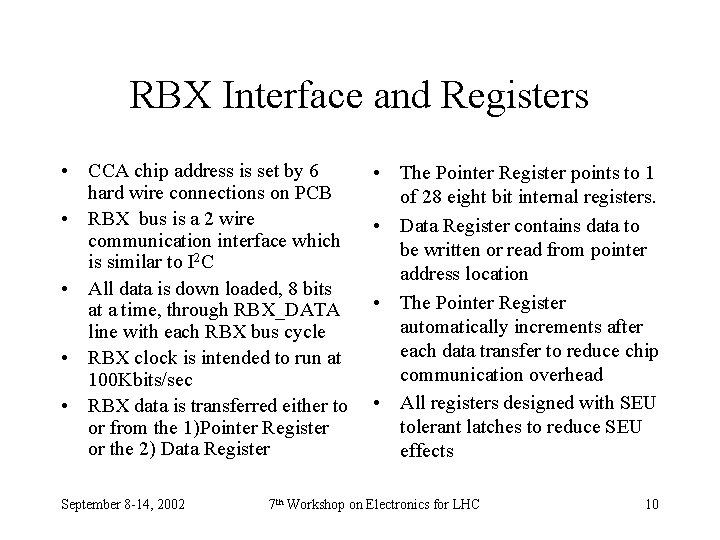
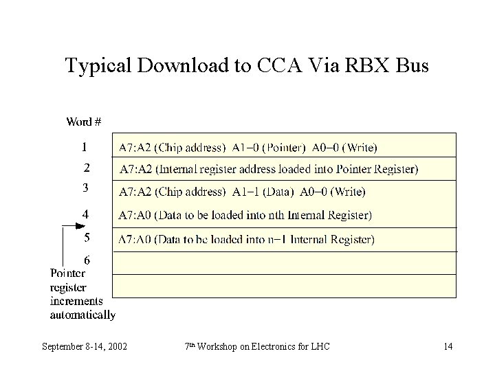
RBX Interface and Registers • CCA chip address is set by 6 hard wire connections on PCB • RBX bus is a 2 wire communication interface which is similar to I 2 C • All data is down loaded, 8 bits at a time, through RBX_DATA line with each RBX bus cycle • RBX clock is intended to run at 100 Kbits/sec • RBX data is transferred either to or from the 1)Pointer Register or the 2) Data Register September 8 -14, 2002 • The Pointer Register points to 1 of 28 eight bit internal registers. • Data Register contains data to be written or read from pointer address location • The Pointer Register automatically increments after each data transfer to reduce chip communication overhead • All registers designed with SEU tolerant latches to reduce SEU effects 7 th Workshop on Electronics for LHC 10

Control Register Space and QIE Clock Adjustment September 8 -14, 2002 7 th Workshop on Electronics for LHC 11

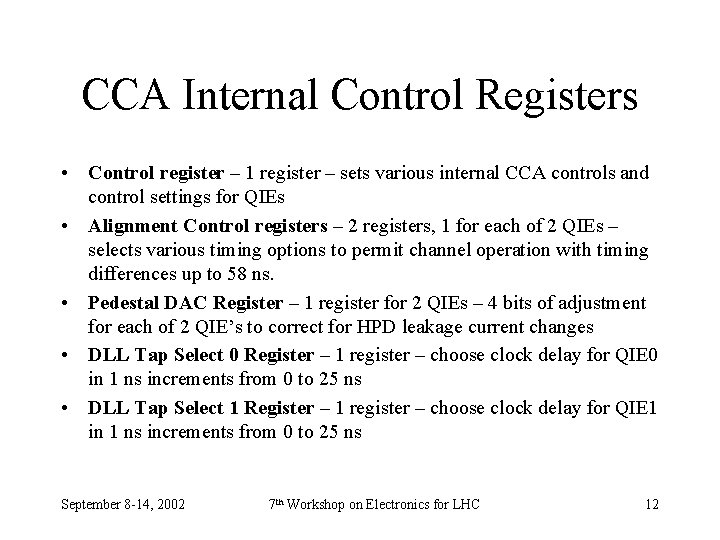
CCA Internal Control Registers • Control register – 1 register – sets various internal CCA controls and control settings for QIEs • Alignment Control registers – 2 registers, 1 for each of 2 QIEs – selects various timing options to permit channel operation with timing differences up to 58 ns. • Pedestal DAC Register – 1 register for 2 QIEs – 4 bits of adjustment for each of 2 QIE’s to correct for HPD leakage current changes • DLL Tap Select 0 Register – 1 register – choose clock delay for QIE 0 in 1 ns increments from 0 to 25 ns • DLL Tap Select 1 Register – 1 register – choose clock delay for QIE 1 in 1 ns increments from 0 to 25 ns September 8 -14, 2002 7 th Workshop on Electronics for LHC 12

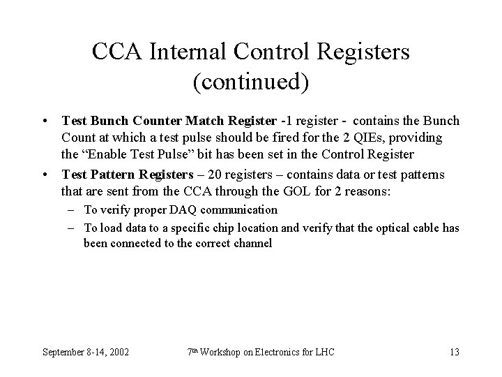
CCA Internal Control Registers (continued) • Test Bunch Counter Match Register -1 register - contains the Bunch Count at which a test pulse should be fired for the 2 QIEs, providing the “Enable Test Pulse” bit has been set in the Control Register • Test Pattern Registers – 20 registers – contains data or test patterns that are sent from the CCA through the GOL for 2 reasons: – To verify proper DAQ communication – To load data to a specific chip location and verify that the optical cable has been connected to the correct channel September 8 -14, 2002 7 th Workshop on Electronics for LHC 13

Typical Download to CCA Via RBX Bus September 8 -14, 2002 7 th Workshop on Electronics for LHC 14

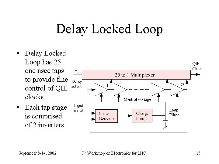
Delay Locked Loop • Delay Locked Loop has 25 one nsec taps to provide fine control of QIE clocks • Each tap stage is comprised of 2 inverters September 8 -14, 2002 7 th Workshop on Electronics for LHC 15

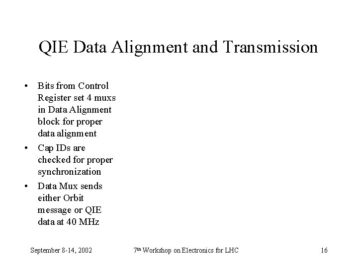
QIE Data Alignment and Transmission • Bits from Control Register set 4 muxs in Data Alignment block for proper data alignment • Cap IDs are checked for proper synchronization • Data Mux sends either Orbit message or QIE data at 40 MHz September 8 -14, 2002 7 th Workshop on Electronics for LHC 16

Typical Data Transmission • When Bunch Crossing Zero is received, an Orbit Message is sent and at the same time the QIEs are reset with Cap ID=0. • QIE data is sent after the Orbit Message September 8 -14, 2002 7 th Workshop on Electronics for LHC 17

Other CCA Circuits • Bunch Counter – 12 bit counter that starts at 0 and increments with the LHC clock. Before reset at next Bunch Crossing=0, counter value is compared to expected value in the Event Checker. Any errors are flagged. The BC value is also stored for transmission in Orbit Message • Test Pulse Trigger Comparator – Produces a Send_Test_Pulse signal when number in the Test Pulse Bunch Count Match Register equals the Bunch Counter number. Pulse is 1 cycle long. Polarity is settable through a bit in the Control Register. • Synchronizer – Synchronizes test pulses for the 2 QIE which have different clock delays so the test pulse occurs in the same time slice. Also Syncs QIE reset pulses. September 8 -14, 2002 7 th Workshop on Electronics for LHC 18

September 8 -14, 2002 7 th Workshop on Electronics for LHC 19

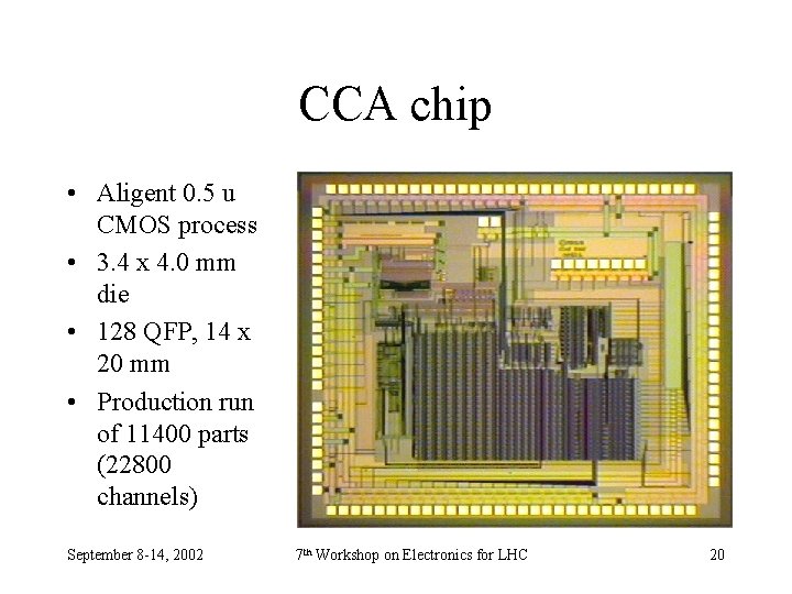
CCA chip • Aligent 0. 5 u CMOS process • 3. 4 x 4. 0 mm die • 128 QFP, 14 x 20 mm • Production run of 11400 parts (22800 channels) September 8 -14, 2002 7 th Workshop on Electronics for LHC 20

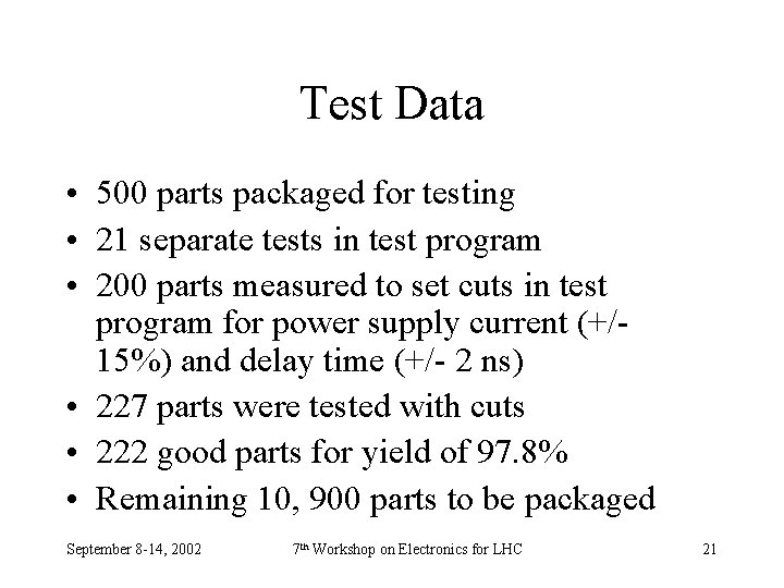
Test Data • 500 parts packaged for testing • 21 separate tests in test program • 200 parts measured to set cuts in test program for power supply current (+/15%) and delay time (+/- 2 ns) • 227 parts were tested with cuts • 222 good parts for yield of 97. 8% • Remaining 10, 900 parts to be packaged September 8 -14, 2002 7 th Workshop on Electronics for LHC 21

Conclusion • Production quantity of CCA has been received for the Hadron Calorimeter • All performance specifications have been met • The CCA has been successfully run on a Front End Module with the QIEs • The yield from testing the first 200 parts is very high. September 8 -14, 2002 7 th Workshop on Electronics for LHC 22

Acknowledgements • The authors want to thank – Abder Mekkaoui for significant contributions throughout the development of the CCA – William Wester and Christian Gingu in the ASIC test group at Fermilab for the yield information that was used – Jim Hoff and Alpana Shenai for layout assistance – Al Dyer for his test assembly assistance September 8 -14, 2002 7 th Workshop on Electronics for LHC 23