Ch 10 MOSFETs and MOS Digital Circuits Examine
- Slides: 26

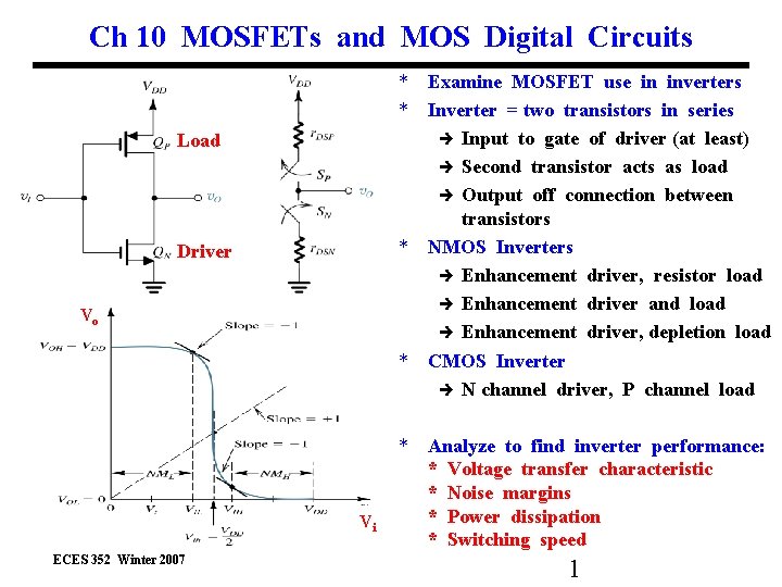
Ch 10 MOSFETs and MOS Digital Circuits * Examine MOSFET use in inverters * Inverter = two transistors in series Input to gate of driver (at least) Second transistor acts as load Output off connection between transistors * NMOS Inverters Enhancement driver, resistor load Enhancement driver and load Enhancement driver, depletion load * CMOS Inverter N channel driver, P channel load Load Driver Vo Vi ECES 352 Winter 2007 * Analyze to find inverter performance: * Voltage transfer characteristic * Noise margins * Power dissipation * Switching speed 1

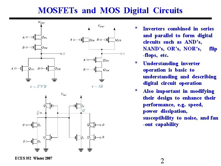
MOSFETs and MOS Digital Circuits * Inverters combined in series and parallel to form digital circuits such as AND’s, NAND’s, OR’s, NOR’s, flip -flops, etc. * Understanding inverter operation is basic to understanding and describing digital circuit operation * Also important in modifying their design to enhance their performance, e. g. speed, power dissipation, susceptibility to noise, and fan -out capability ECES 352 Winter 2007 2

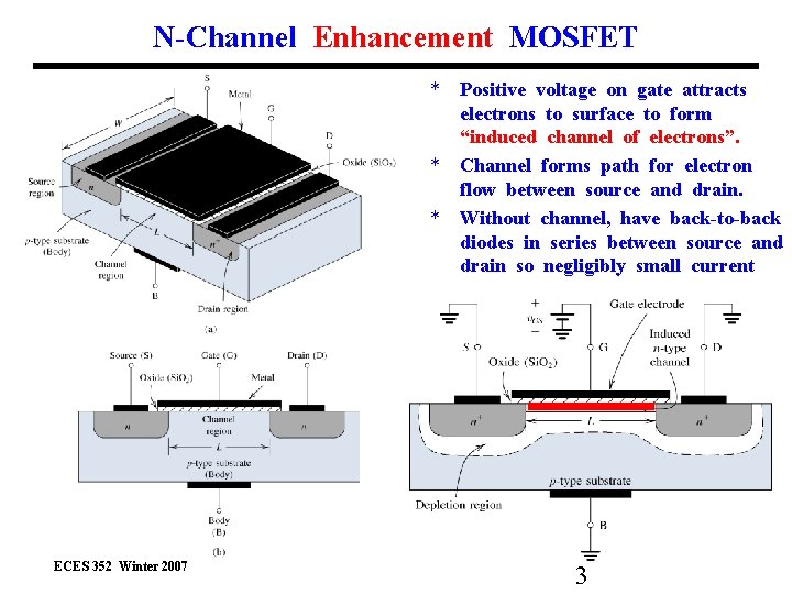
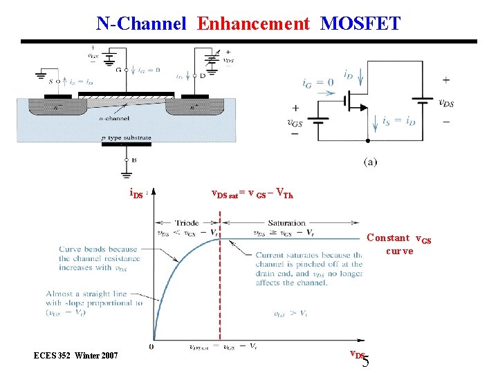
N-Channel Enhancement MOSFET * Positive voltage on gate attracts electrons to surface to form “induced channel of electrons”. * Channel forms path for electron flow between source and drain. * Without channel, have back-to-back diodes in series between source and drain so negligibly small current ECES 352 Winter 2007 3

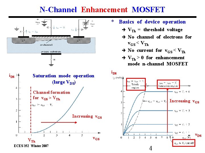
N-Channel Enhancement MOSFET * Basics of device operation i. DS Saturation mode operation (large VDS) VTh = threshold voltage No channel of electrons for v. GS < VTh No current for v. GS < VTh > 0 for enhancement mode n-channel MOSFET i. DS Channel formation for v. GS > VTh Increasing v. GS VTh ECES 352 Winter 2007 v. DS v. GS 4

N-Channel Enhancement MOSFET i. DS v. DS sat = v GS – VTh Constant v. GS curve ECES 352 Winter 2007 v. DS 5

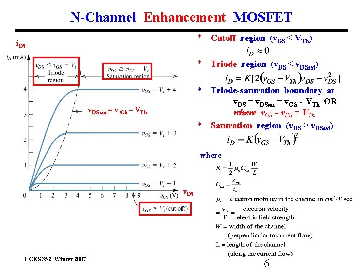
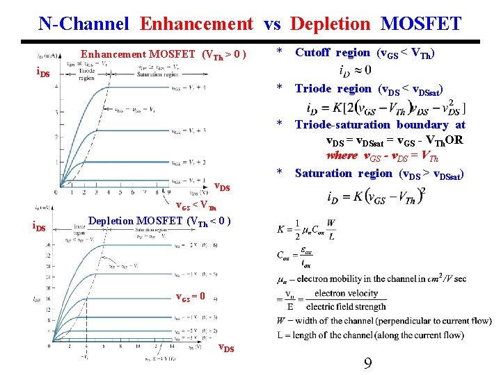
N-Channel Enhancement MOSFET * Cutoff region (v. GS < VTh) i. DS * Triode region (v. DS < v. DSsat) * Triode-saturation boundary at v. DS = v. DSsat = v. GS - VTh OR where v. GS - v. DS = VTh * Saturation region (v. DS > v. DSsat) v. DS sat = v GS – VTh where v. DS ECES 352 Winter 2007 6

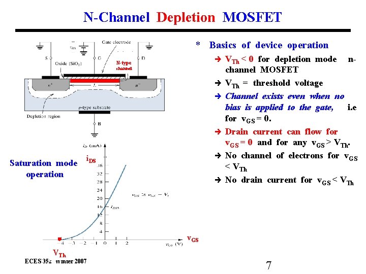
N-Channel Depletion MOSFET * Basics of device operation N-type channel Saturation mode operation i. DS VTh < 0 for depletion mode nchannel MOSFET VTh = threshold voltage Channel exists even when no bias is applied to the gate, i. e for v. GS = 0. Drain current can flow for v. GS = 0 and for any v. GS > VTh. No channel of electrons for v. GS < VTh No drain current for v. GS < VTh v. GS VTh ECES 352 Winter 2007 7

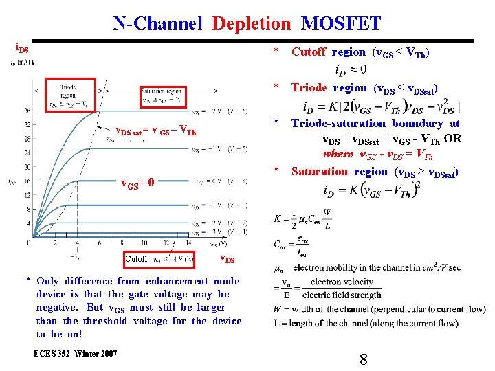
N-Channel Depletion MOSFET i. DS * Cutoff region (v. GS < VTh) * Triode region (v. DS < v. DSsat) * Triode-saturation boundary at v. DS = v. DSsat = v. GS - VTh OR where v. GS - v. DS = VTh * Saturation region (v. DS > v. DSsat) v. DS sat = v GS – VTh v. GS= 0 Cutoff v. DS * Only difference from enhancement mode device is that the gate voltage may be negative. But v. GS must still be larger than the threshold voltage for the device to be on! ECES 352 Winter 2007 8

N-Channel Enhancement vs Depletion MOSFET Enhancement MOSFET (VTh > 0 ) * Cutoff region (v. GS < VTh) i. DS * Triode region (v. DS < v. DSsat) v. DS * Triode-saturation boundary at v. DS = v. DSsat = v. GS - VTh. OR where v. GS - v. DS = VTh * Saturation region (v. DS > v. DSsat) v. GS < VTh i. DS Depletion MOSFET (VTh < 0 ) v. GS = 0 ECES 352 Winter 2007 v. DS 9

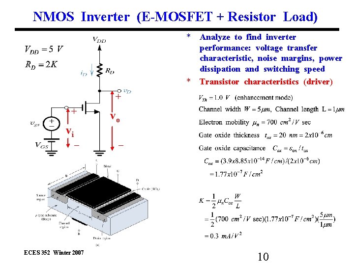
NMOS Inverter (E-MOSFET + Resistor Load) * Analyze to find inverter performance: voltage transfer characteristic, noise margins, power dissipation and switching speed * Transistor characteristics (driver) + + vi _ ECES 352 Winter 2007 vo _ 10

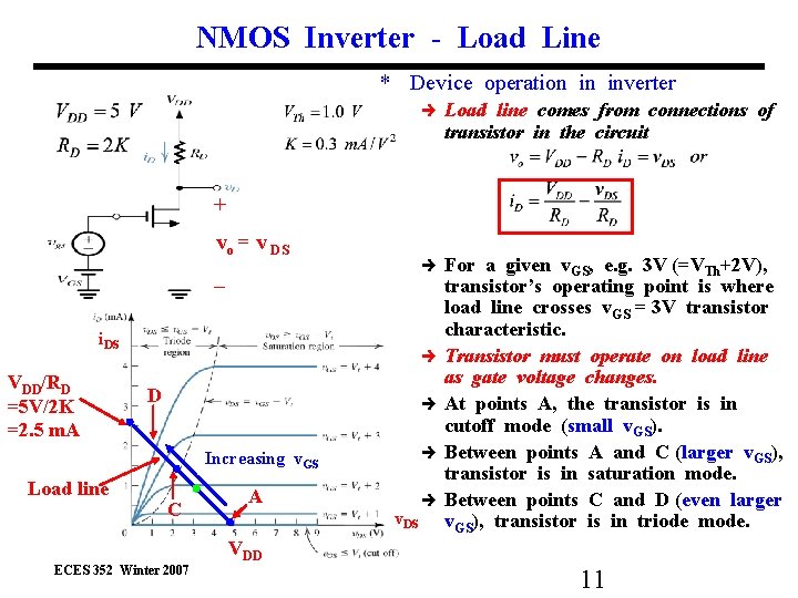
NMOS Inverter - Load Line * Device operation in inverter Load line comes from connections of transistor in the circuit For a given v. GS, e. g. 3 V (=VTh+2 V), transistor’s operating point is where load line crosses v. GS = 3 V transistor characteristic. Transistor must operate on load line as gate voltage changes. At points A, the transistor is in cutoff mode (small v. GS). Between points A and C (larger v. GS), transistor is in saturation mode. Between points C and D (even larger v. GS), transistor is in triode mode. + vo = v DS _ i. DS VDD/RD =5 V/2 K =2. 5 m. A D Increasing v. GS Load line C . A v. DS VDD ECES 352 Winter 2007 11

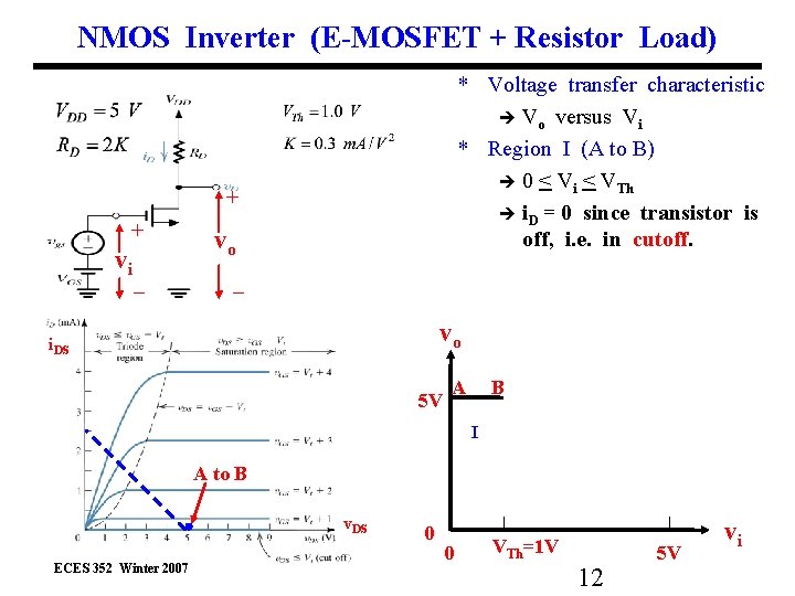
NMOS Inverter (E-MOSFET + Resistor Load) * Voltage transfer characteristic Vo versus Vi * Region I (A to B) 0 < Vi < VTh i. D = 0 since transistor is off, i. e. in cutoff. + + vi vo _ _ vo i. DS 5 V A B I A to B . ECES 352 Winter 2007 v. DS 0 0 VTh=1 V 12 5 V vi

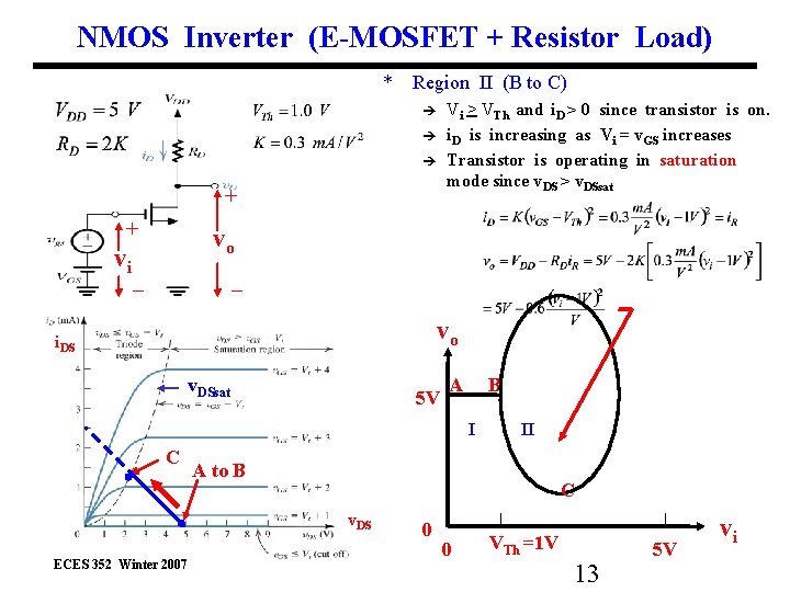
NMOS Inverter (E-MOSFET + Resistor Load) * Region II (B to C) + + vi Vi > VTh and i. D > 0 since transistor is on. i. D is increasing as Vi = v. GS increases Transistor is operating in saturation mode since v. DS > v. DSsat vo _ _ vo i. DS v. DSsat 5 V A B I C . ECES 352 Winter 2007 II A to B C v. DS 0 0 VTh =1 V 13 5 V vi

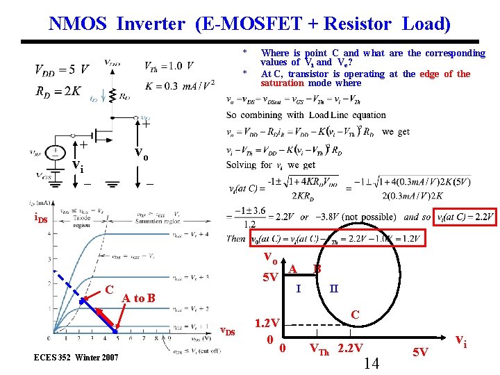
NMOS Inverter (E-MOSFET + Resistor Load) * * Where is point C and what are the corresponding values of Vi and Vo? At C, transistor is operating at the edge of the saturation mode where + + vi vo _ _ i. DS vo C . ECES 352 Winter 2007 A 5 V I A to B v. DS 1. 2 V 0 B II C 0 VTh 2. 2 V 14 5 V vi

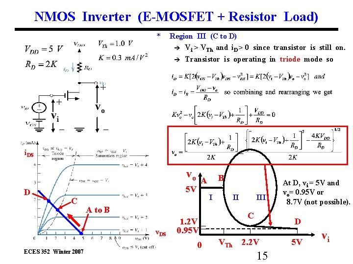
NMOS Inverter (E-MOSFET + Resistor Load) * Region III (C to D) Vi > VTh and i. D > 0 since transistor is still on. Transistor is operating in triode mode so + + vi vo _ _ i. DS vo D 5 V C B A I II A to B . ECES 352 Winter 2007 v. DS C 1. 2 V 0. 95 V 0 III VTh At D, vi = 5 V and vo= 0. 95 V or 8. 7 V (not possible). D 2. 2 V 15 5 V vi

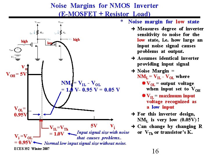
Noise Margins for NMOS Inverter (E-MOSFET + Resistor Load) * Noise margin for low state high low vo VOH = 5 V NML= VIL - VOL = 1. 0 V- 0. 95 V = 0. 05 V VOL= 0. 95 V Vi =VOL = 0. 95 V VIL=VTh = 1. 0 V 5 V vi Input signal size with noise that causes problems. . Normal low input signal size without noise. ECES 352 Winter 2007 Measures degree of inverter sensitivity to noise for the low state, i. e. how large an input noise signal causes problems at output. Assumes identical inverter providing input signal Noise Margin = NML = VIL - VOL where VOL = output voltage when input set to VOH VIL = maximum input voltage recognized as a low input For this inverter design, NML is very low (0. 05 V) ! Can change by changing R or VTh or transistor’s K. 16

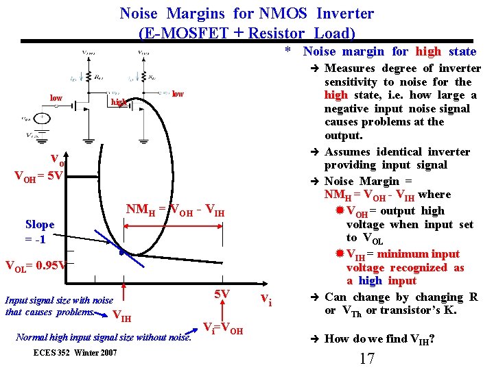
Noise Margins for NMOS Inverter (E-MOSFET + Resistor Load) * Noise margin for high state low high low vo VOH = 5 V Slope = -1 NMH = VOH - VIH VOL= 0. 95 V Input signal size with noise that causes problems. V 5 V IH Normal high input signal size without noise. ECES 352 Winter 2007 Vi=VOH vi Measures degree of inverter sensitivity to noise for the high state, i. e. how large a negative input noise signal causes problems at the output. Assumes identical inverter providing input signal Noise Margin = NMH = VOH - VIH where VOH = output high voltage when input set to VOL VIH = minimum input voltage recognized as a high input Can change by changing R or VTh or transistor’s K. How do we find VIH? 17

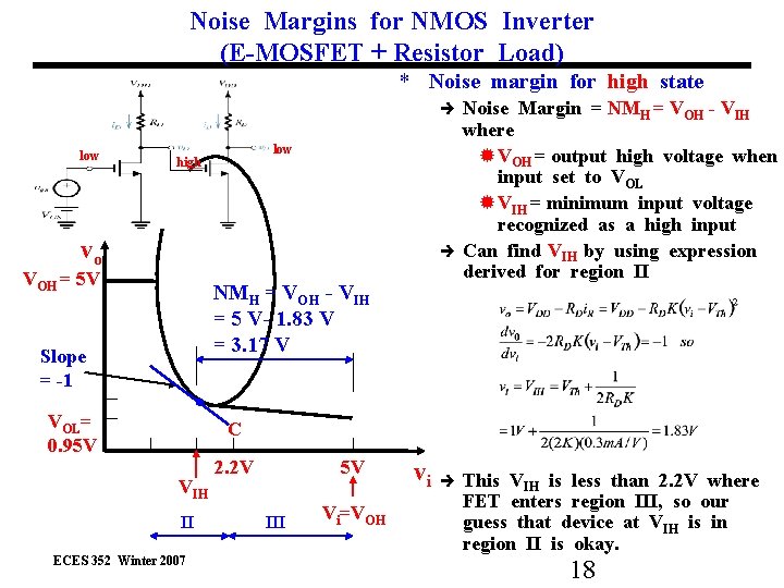
Noise Margins for NMOS Inverter (E-MOSFET + Resistor Load) * Noise margin for high state low high vo VOH = 5 V NMH = VOH - VIH = 5 V- 1. 83 V = 3. 17 V Slope = -1 VOL= 0. 95 V Noise Margin = NMH = VOH - VIH where VOH = output high voltage when input set to VOL VIH = minimum input voltage recognized as a high input Can find VIH by using expression derived for region II C VIH II ECES 352 Winter 2007 2. 2 V 5 V III Vi=VOH vi This VIH is less than 2. 2 V where FET enters region III, so our guess that device at VIH is in region II is okay. 18

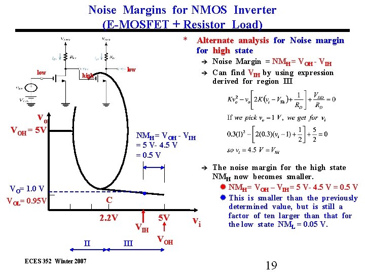
Noise Margins for NMOS Inverter (E-MOSFET + Resistor Load) * Alternate analysis for Noise margin for high state low high Noise Margin = NMH = VOH - VIH Can find VIH by using expression derived for region III vo VOH = 5 V NMH = VOH - VIH = 5 V- 4. 5 V = 0. 5 V VO= 1. 0 V VOL= 0. 95 V C 2. 2 V II ECES 352 Winter 2007 VIH III 5 V vi The noise margin for the high state NMH now becomes smaller. NMH = VOH – VIH = 5 V- 4. 5 V = 0. 5 V This is smaller than the previously determined value, but is still a factor of ten larger than that for the low state NML = 0. 05 V. VOH 19

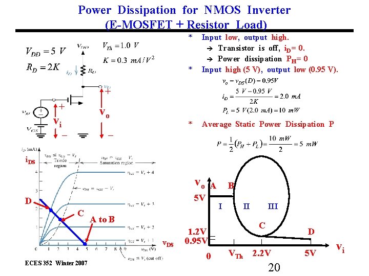
Power Dissipation for NMOS Inverter (E-MOSFET + Resistor Load) * * Input low, output high. Transistor is off, i. D = 0. Power dissipation PH = 0 Input high (5 V), output low (0. 95 V). * Average Static Power Dissipation P + + vi vo _ _ i. DS vo A 5 V D C . ECES 352 Winter 2007 B I II A to B v. DS C 1. 2 V 0. 95 V 0 III VTh D 2. 2 V 20 5 V vi

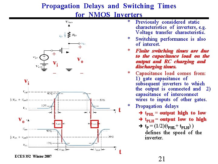
Propagation Delays and Switching Times for NMOS Inverters + + vi _ vo _ vi t vo ECES 352 Winter 2007 t * Previously considered static characteristics of inverters, e. g. Voltage transfer characteristic. * Switching performance is also of interest. * Finite switching times are due to the capacitance load on the output and RC charging and discharging times. * Capacitance load comes from: 1) gate capacitance of subsequent inverters to which the output is connected and 2) capacitance of interconnect wires to inputs of other gates. * Propagation delays t. PHL = output high to low t. PLH = output low to high t. P = (1/2)(t. PHL+ t. PLH) ) defines the speed of the inverter. 21

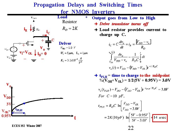
Propagation Delays and Switching Times for NMOS Inverters Load i. R + vi=VOL _ * Output goes from Low to High Drive transistor turns off Load resistor provides current to charge up C. i. C + vo C Driver i. D = 0 _ t. PLH = time to charge to the midpoint ½(VOH+VOL) = 1/2(5 V + 0. 95 V) = 3. 0 V vo VDD 3 V VOL= 0. 95 V t. PLH t ECES 352 Winter 2007 22

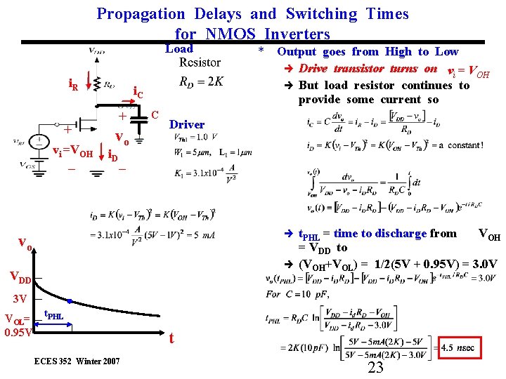
Propagation Delays and Switching Times for NMOS Inverters Load i. R + vi =VOH _ i. C + vo i. D C * Output goes from High to Low Drive transistor turns on v = V i OH But load resistor continues to provide some current so Driver _ t. PHL vo VDD = time to discharge from VOH = VDD to (VOH+VOL) = 1/2(5 V + 0. 95 V) = 3. 0 V 3 V VOL= 0. 95 V t. PHL t ECES 352 Winter 2007 23

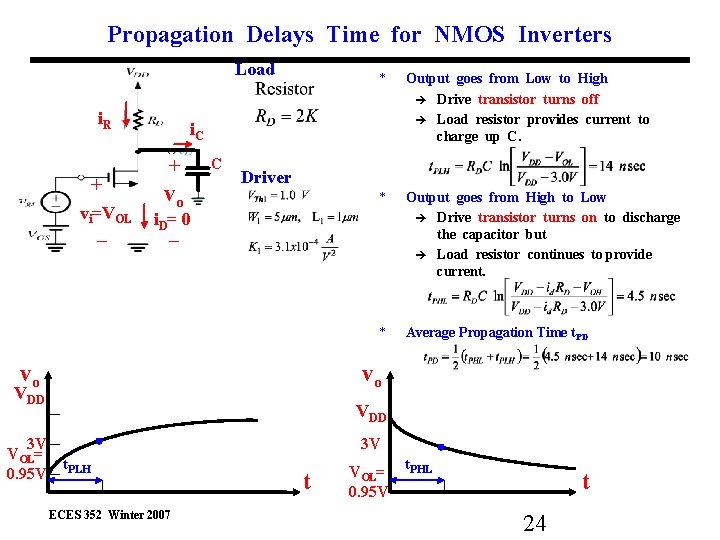
Propagation Delays Time for NMOS Inverters Load i. R + vi=VOL _ Output goes from Low to High Drive transistor turns off Load resistor provides current to charge up C. * Output goes from High to Low Drive transistor turns on to discharge the capacitor but Load resistor continues to provide current. * Average Propagation Time t. PD i. C + vo C Driver i. D = 0 _ vo vo VDD 3 V VOL= 0. 95 V * VDD 3 V t. PLH ECES 352 Winter 2007 t VOL= 0. 95 V t. PHL t 24

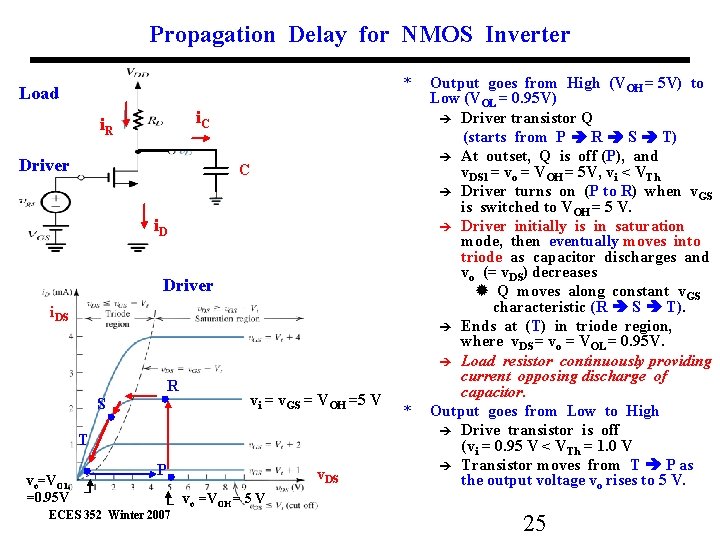
Propagation Delay for NMOS Inverter * Load i. C i. R Driver C i. D Driver i. DS R S vi = v. GS = VOH =5 V T vo=VOL =0. 95 V P ECES 352 Winter 2007 v. DS vo =VOH = 5 V * Output goes from High (VOH = 5 V) to Low (VOL = 0. 95 V) Driver transistor Q (starts from P R S T) At outset, Q is off (P), and v. DS 1 = vo = VOH = 5 V, vi < VTh Driver turns on (P to R) when v. GS is switched to VOH = 5 V. Driver initially is in saturation mode, then eventually moves into triode as capacitor discharges and vo (= v. DS) decreases Q moves along constant v. GS characteristic (R S T). Ends at (T) in triode region, where v. DS = vo = VOL = 0. 95 V. Load resistor continuously providing current opposing discharge of capacitor. Output goes from Low to High Drive transistor is off (vi = 0. 95 V < VTh = 1. 0 V Transistor moves from T P as the output voltage vo rises to 5 V. 25

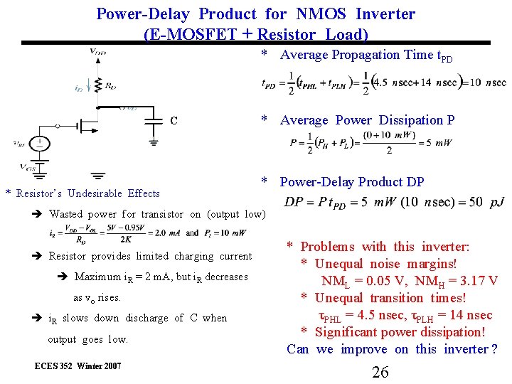
Power-Delay Product for NMOS Inverter (E-MOSFET + Resistor Load) * Average Propagation Time t. PD C * Resistor’s Undesirable Effects * Average Power Dissipation P * Power-Delay Product DP Wasted power for transistor on (output low) Resistor provides limited charging current Maximum i. R = 2 m. A, but i. R decreases as vo rises. i. R slows down discharge of C when output goes low. ECES 352 Winter 2007 * Problems with this inverter: * Unequal noise margins! NML = 0. 05 V, NMH = 3. 17 V * Unequal transition times! τPHL = 4. 5 nsec, τPLH = 14 nsec * Significant power dissipation! Can we improve on this inverter ? 26