Cell Broadband Engine Cell Broadband Engine Structure PPE

Cell Broadband Engine
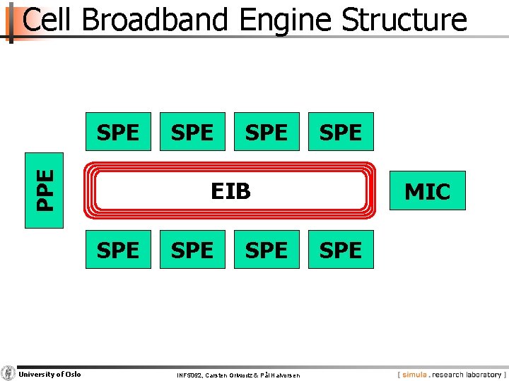
Cell Broadband Engine Structure PPE SPE SPE EIB SPE University of Oslo SPE SPE INF 5062, Carsten Griwodz & Pål Halvorsen MIC SPE

Cell Broadband Engine Structure PPE SPE SPE EIB SPE SPE MIC SPE PPE - Power Processing Element SPE - Synergistic Processing Element MIC - Memory Interface Controller EIB - Element Interconnect Bus University of Oslo INF 5062, Carsten Griwodz & Pål Halvorsen
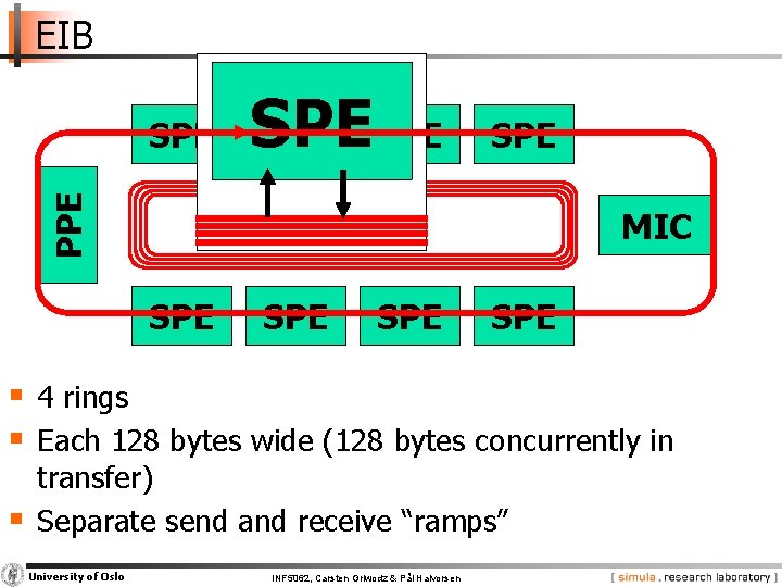
EIB PPE SPE SPE SPE EIB SPE SPE MIC SPE § 4 rings § Each 128 bytes wide (128 bytes concurrently in § transfer) Separate send and receive “ramps” University of Oslo INF 5062, Carsten Griwodz & Pål Halvorsen
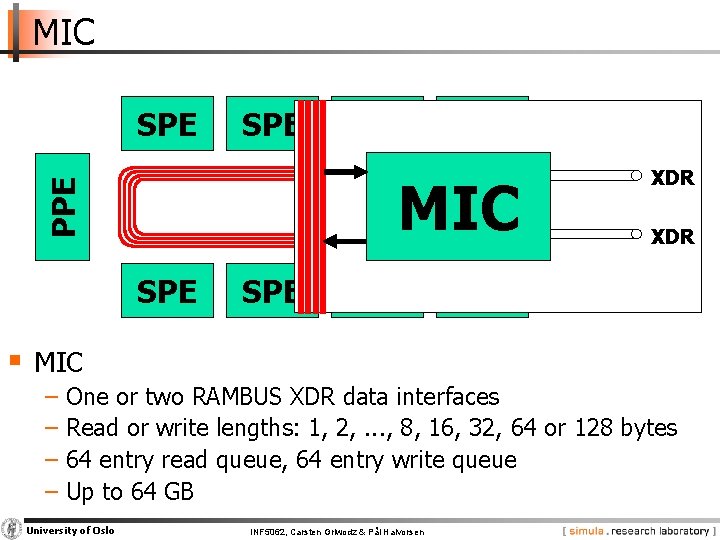
MIC PPE SPE SPE EIB SPE SPE MIC XDR SPE § MIC − One or two RAMBUS XDR data interfaces − Read or write lengths: 1, 2, . . . , 8, 16, 32, 64 or 128 bytes − 64 entry read queue, 64 entry write queue − Up to 64 GB University of Oslo INF 5062, Carsten Griwodz & Pål Halvorsen

Cell Broadband Engine Structure § PPE − Power processing element § PPU − Power processing unit − 32 k. B L 1 instruction cache − 32 k. B L 2 data cache § PPSS − Power. PC processor storage subsystem − 512 k. B unified L 2 cache − EIB accesses are sequential and ordered University of Oslo PPE PPU L 1 instr L 1 data cache PPSS INF 5062, Carsten Griwodz & Pål Halvorsen ≤ 32 byte L 2 cache ≤ 16 byte

Cell Broadband Engine Structure § PPU − 2 -way symmetric multithreading § Duplicated register set − 32 64 -bit general purpose registers − 32 64 -bit floating point registers − 32 128 -bit vector registers − 1 link register for branching − 1 count register for loop count or branching PPE PPU registers integer L 1 instr L 1 data 32 GP link cache count cond exp float PPSS ctrl FP ≤ 32 byte ≤ 16 32 byte vector L 2 vector ctrl sav/rstr cache University of Oslo INF 5062, Carsten Griwodz & Pål Halvorsen 32

Cell Broadband Engine Structure SPE § SPE − Synergetic processing element SPU § SPU . . . − Synergetic processing unit − 4 execution units (for 4 hardware contexts) − RF: register file − LS: local store § MFC: Memory flow controller RF MFC MMIO registers − MMIO registers: memory mapped I/O registers − DMA controller University of Oslo LS INF 5062, Carsten Griwodz & Pål Halvorsen DMA controller
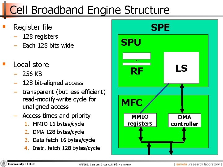
Cell Broadband Engine Structure SPE § Register file − 128 registers − Each 128 bits wide SPU. . . § Local store − 256 KB − 128 bit-aligned access − transparent (but less efficient) read-modify-write cycle for unaligned access − Access times and priority 1. 2. 3. 4. MMIO 16 bytes/cycle DMA 128 bytes/cycle Data fetch 16 bytes/cycle Instr. fetch 128 bytes/cycle University of Oslo RF LS MFC MMIO registers INF 5062, Carsten Griwodz & Pål Halvorsen DMA controller

Cell Broadband Engine Structure SPE § DMA controller − Can have 16 DMA operations concurrently in flight, more than normal CPUs (i. e. 128 total) − Transfer size up to 16 KB for each operation SPU. . . RF LS § Mailboxes − 32 -bit dedicated registers − Implemented as channels − Used for communication with PPE − 2 outgoing mailboxes − 1 incoming mailbox University of Oslo MFC MMIO registers INF 5062, Carsten Griwodz & Pål Halvorsen DMA controller
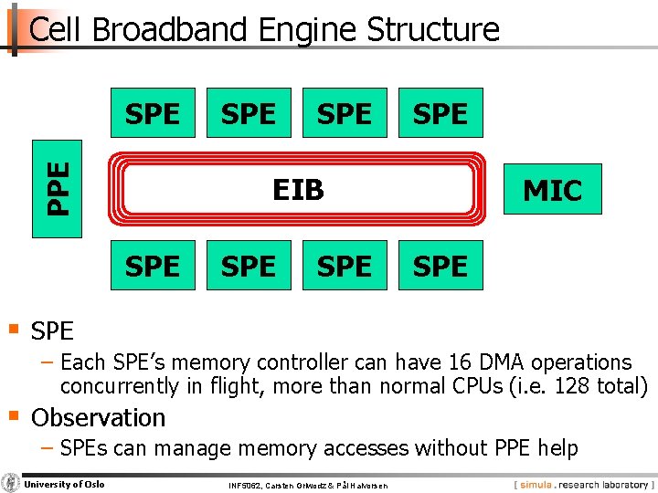
Cell Broadband Engine Structure PPE SPE SPE EIB SPE SPE MIC SPE § SPE − Each SPE’s memory controller can have 16 DMA operations concurrently in flight, more than normal CPUs (i. e. 128 total) § Observation − SPEs can manage memory accesses without PPE help University of Oslo INF 5062, Carsten Griwodz & Pål Halvorsen

Cell Broadband Engine Structure § either − 64 bit flat address space − no mapping of local store to PPE address space mem § or SPE − virtual addressing − 42 bit real address space mem SPE PPE • independently set up for data and instruction addressing EIB − 64 bit effective address space MIC − 65 bit virtual address space SPEsizes § 256 MB segment SPE − Mappable mem from 65 -bit space memto 42 - mem bit space SPE mem § 4 k. B and 2 of (16 k. B, 1 MB, 16 MB) page sizes Flat address space of the PPE − swappable University of Oslo INF 5062, Carsten Griwodz & Pål Halvorsen mem
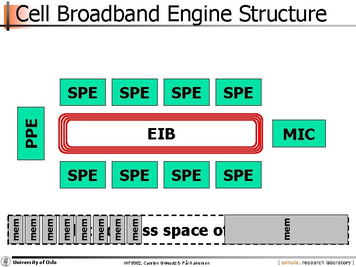
Cell Broadband Engine Structure University of Oslo SPE mem mem SPE EIB SPE mem SPE MIC SPE mem SPE PPE SPE Flat address space of the PPE INF 5062, Carsten Griwodz & Pål Halvorsen
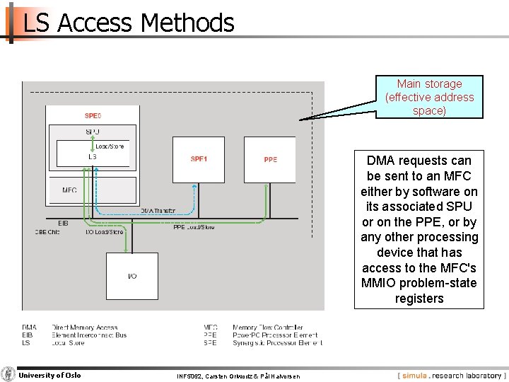
LS Access Methods Main storage (effective address space) DMA requests can be sent to an MFC either by software on its associated SPU or on the PPE, or by any other processing device that has access to the MFC's MMIO problem-state registers University of Oslo INF 5062, Carsten Griwodz & Pål Halvorsen
n. VIDIA
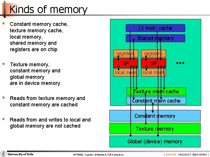
Kinds of memory § Constant memory cache, L 1 instr. cache texture memory cache, local memory, shared memory and registers are on chip Shared memory § Texture memory, constant memory and global memory are in device memory registers SP SP local mem § Reads from texture memory and constant memory are cached § Reads from and writes to local and global memory are not cached . . . Texture mem cache Constant memory Texture memory Global (device) memory University of Oslo INF 5062, Carsten Griwodz & Pål Halvorsen
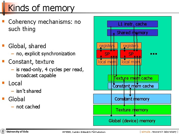
Kinds of memory § Coherency mechanisms: no L 1 instr. cache such thing Shared memory § Global, shared − no, explicit synchronization § Constant, texture registers SP SP local mem − is read-only, 4 cycles per read, broadcast capable § Local . . . Texture mem cache Constant mem cache − isn’t shared § Global Constant memory − not cached Texture memory Global (device) memory University of Oslo INF 5062, Carsten Griwodz & Pål Halvorsen
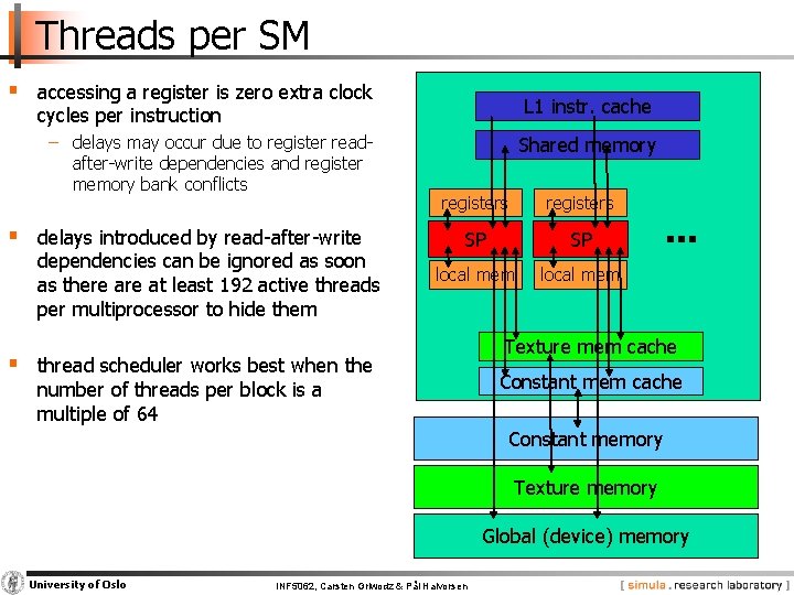
Threads per SM § accessing a register is zero extra clock L 1 instr. cache cycles per instruction − delays may occur due to register readafter-write dependencies and register memory bank conflicts § delays introduced by read-after-write dependencies can be ignored as soon as there at least 192 active threads per multiprocessor to hide them Shared memory registers SP SP local mem § thread scheduler works best when the number of threads per block is a multiple of 64 . . . Texture mem cache Constant memory Texture memory Global (device) memory University of Oslo INF 5062, Carsten Griwodz & Pål Halvorsen
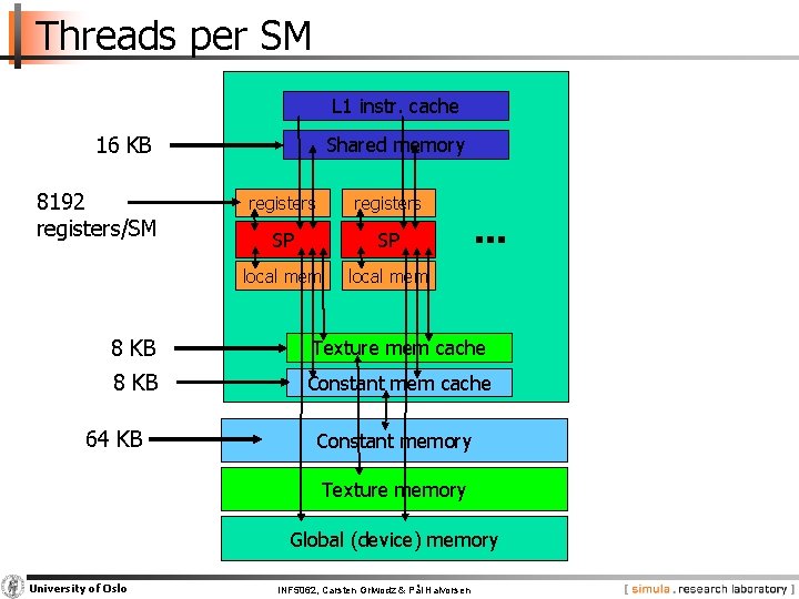
Threads per SM L 1 instr. cache 16 KB 8192 registers/SM Shared memory registers SP SP local mem . . . 8 KB Texture mem cache 8 KB Constant mem cache 64 KB Constant memory Texture memory Global (device) memory University of Oslo INF 5062, Carsten Griwodz & Pål Halvorsen
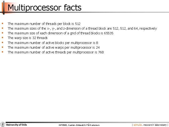
Multiprocessor facts § § § § The The maximum number of threads per block is 512 maximum sizes of the x-, y-, and z-dimension of a thread block are 512, and 64, respectively maximum size of each dimension of a grid of thread blocks is 65535 warp size is 32 threads maximum number of active blocks per multiprocessor is 8 maximum number of active warps per multiprocessor is 24 maximum number of active threads per multiprocessor is 768 University of Oslo INF 5062, Carsten Griwodz & Pål Halvorsen

Threads per SM § accessing a register is zero extra clock L 1 instr. cache cycles per instruction − delays may occur due to register readafter-write dependencies and register memory bank conflicts § delays introduced by read-after-write dependencies can be ignored as soon as there at least 192 active threads per multiprocessor to hide them Shared memory registers SP SP local mem § thread scheduler works best when the number of threads per block is a multiple of 64 . . . Texture mem cache Constant memory Texture memory Global (device) memory University of Oslo INF 5062, Carsten Griwodz & Pål Halvorsen
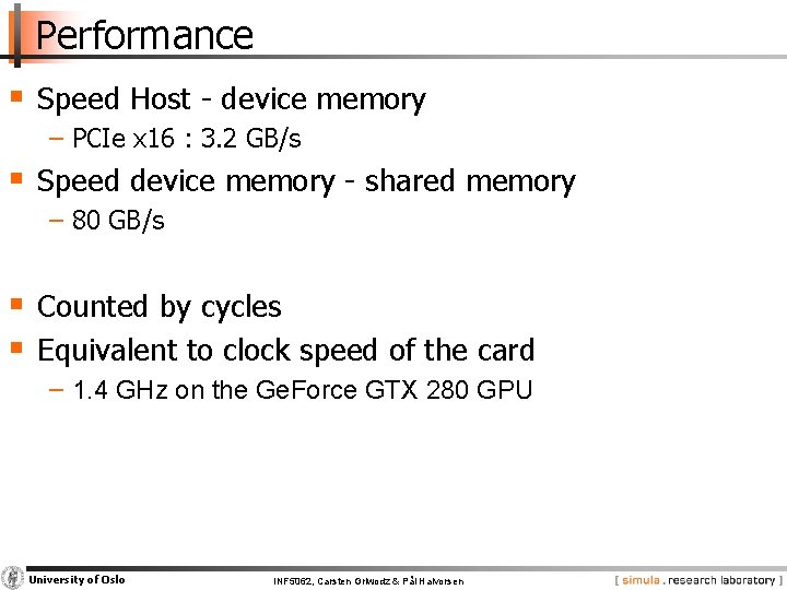
Performance § Speed Host - device memory − PCIe x 16 : 3. 2 GB/s § Speed device memory - shared memory − 80 GB/s § Counted by cycles § Equivalent to clock speed of the card − 1. 4 GHz on the Ge. Force GTX 280 GPU University of Oslo INF 5062, Carsten Griwodz & Pål Halvorsen
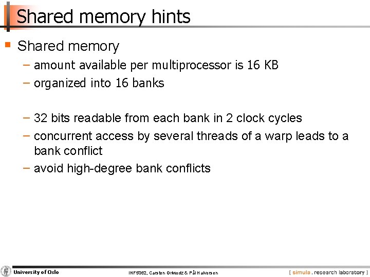
Shared memory hints § Shared memory − amount available per multiprocessor is 16 KB − organized into 16 banks − 32 bits readable from each bank in 2 clock cycles − concurrent access by several threads of a warp leads to a bank conflict − avoid high-degree bank conflicts University of Oslo INF 5062, Carsten Griwodz & Pål Halvorsen
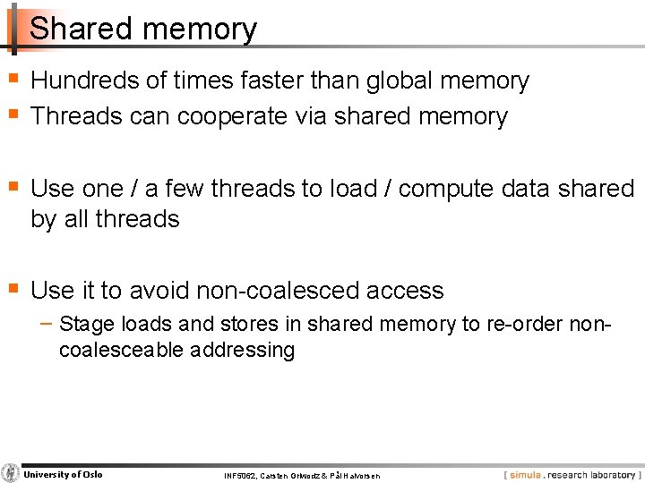
Shared memory § Hundreds of times faster than global memory § Threads can cooperate via shared memory § Use one / a few threads to load / compute data shared by all threads § Use it to avoid non-coalesced access − Stage loads and stores in shared memory to re-order noncoalesceable addressing University of Oslo INF 5062, Carsten Griwodz & Pål Halvorsen
GOOD University of Oslo BAD INF 5062, Carsten Griwodz & Pål Halvorsen
BAD University of Oslo INF 5062, Carsten Griwodz & Pål Halvorsen
Coalescing § Coalescing − fast, bursty transfer between multiple registers allocated to different threads in the same warp − if per-thread memory accesses for a single warp (today’s hardware actual half-warp) form a contiguous range of addresses, accesses will be coalesced into a single access − is not a dynamic ability − compiler must identify it and generate appropriate code − occurs when thread n accessed “base-address + size * n”, where • base-address is aligned to 16 * size • size of the read operation: 4, 8 or 16 bytes University of Oslo INF 5062, Carsten Griwodz & Pål Halvorsen
Memory latency and features § Read from global memory − 16 -bit aligned, otherwise read-modify-write − 32 -bit, 64 -bit, 128 -bit read operations supported § Coalesced read − If all threads in a warp read concurrently in a pattern, reads are “coalesced” − coalesced read of 32 bits per thread is slighter faster than coalesced read of 64 bits per thread and much faster than coalesced read of 128 bits per thread − but all are warpsize times faster than non-coalesced reads University of Oslo INF 5062, Carsten Griwodz & Pål Halvorsen

Device (global) Memory hints § Device memory − coalesced vs. non-coalesced access times differ by an order of magnitude § Global/Local device memory University of Oslo INF 5062, Carsten Griwodz & Pål Halvorsen
Memory access § Access to device memory is slow − 4 cycles to set up, 400 to 600 cycles to complete § Use multithreading to use that time § Partition your computation to keep the GPU multiprocessors equally busy − Many threads, many thread blocks § Keep resource usage low enough to support multiple active thread blocks per multiprocessor − Registers, shared memory University of Oslo INF 5062, Carsten Griwodz & Pål Halvorsen
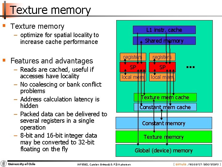
Texture memory § Texture memory L 1 instr. cache − optimize for spatial locality to increase cache performance § Features and advantages − Reads are cached, useful if accesses have locality − No coalescing or bank conflict problems − Address calculation latency is hidden − Packed data can be delivered to several registers in a single operation − 8 -bit and 16 -bit integer data may be converted to 32 -bit floating on the fly University of Oslo Shared memory registers SP SP local mem INF 5062, Carsten Griwodz & Pål Halvorsen . . . Texture mem cache Constant memory Texture memory Global (device) memory
Texture memory raw facts § cache working set is 8 KB per multiprocessor § texture reference bound to a one-dimensional CUDA § § array: maximum width 213 texture reference bound to a two-dimensional CUDA array: maximum width 216 maximum height 215 texture reference bound to linear memory: maximum width 227 University of Oslo INF 5062, Carsten Griwodz & Pål Halvorsen
Optimization priorities § Memory coalescing has highest priority − Largest effect − Optimize for locality § Take advantage of shared memory − Very high bandwidth − Threads can cooperate to save work § Use parallelism efficiently − Keep the GPU busy at all times − High arithmetic / bandwidth ratio − Many threads & thread blocks § Leave bank conflicts for last − 4 -way and smaller conflicts are not usually worth avoiding if avoiding them will cost more instructions University of Oslo INF 5062, Carsten Griwodz & Pål Halvorsen
- Slides: 33