CELIA A Device and Architecture CoDesign Framework for






- Slides: 27

CELIA: A Device and Architecture Co-Design Framework for STT-MRAM-Based Deep Learning Acceleration Hao Yan, Hebin R. Cherian, Ethan C. Ahn and Lide Duan Department of Electrical and Computer Engineering University of Texas at San Antonio The University of Texas at San Antonio, One UTSA Circle, San Antonio, TX 78249

Deep Learning Applications • Deep learning has recently shown extensive usage in a wide variety of applications: – Image/speech recognition, self-driving cars, financial services, healthcare – Great success of CNNs in image classification • The recent success of deep learning is due to: – Information available for model training – Fast increase of computing capacity – Development of large open-source frameworks The University of Texas at San Antonio, One UTSA Circle, San Antonio, TX 78249 2

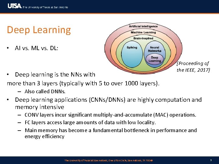
Deep Learning • AI vs. ML vs. DL: • Deep learning is the NNs with more than 3 layers (typically with 5 to over 1000 layers). [Proceeding of the IEEE, 2017] – Also called DNNs. • Deep learning applications (CNNs/DNNs) are highly computation and memory intensive – CONV layers incur significant multiply-and-accumulate (MAC) operations. – FC layers access large amounts of data with low locality. – Main memory has become a fundamental bottleneck in performance and energy efficiency The University of Texas at San Antonio, One UTSA Circle, San Antonio, TX 78249 3

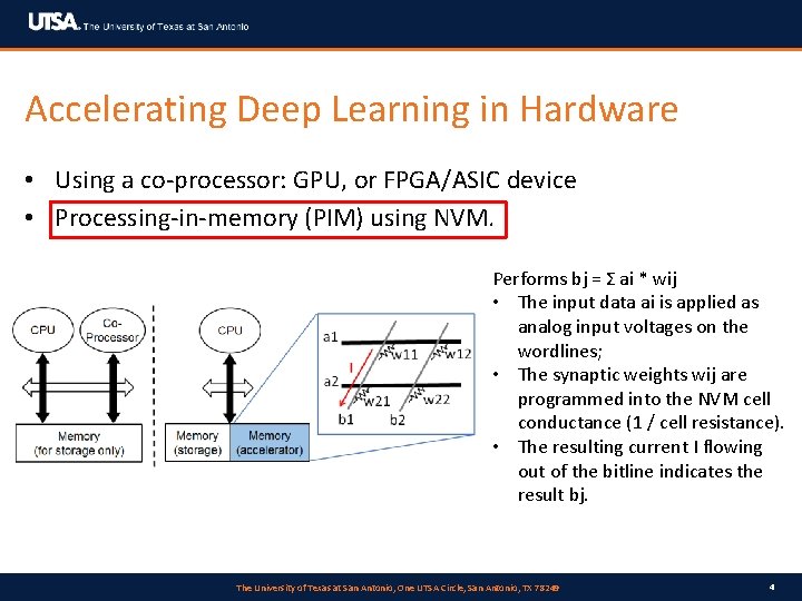
Accelerating Deep Learning in Hardware • Using a co-processor: GPU, or FPGA/ASIC device • Processing-in-memory (PIM) using NVM. Performs bj = Σ ai * wij • The input data ai is applied as analog input voltages on the wordlines; • The synaptic weights wij are programmed into the NVM cell conductance (1 / cell resistance). • The resulting current I flowing out of the bitline indicates the result bj. The University of Texas at San Antonio, One UTSA Circle, San Antonio, TX 78249 4

NVM-Based Deep Learning Acceleration • Utilizes unique features of NVM for computing: – Resistance-based weight storage in crossbar cells – Current-based sensing (enabling analog current computing) • Most of the existing NVM-based accelerators rely on Resistive RAM (RRAM/Re. RAM/memristors): – – SPINDLE [ISLPED 14] PRIME [ISCA 16] ISAAC [ISCA 16] Pipe. Layer [HPCA 17] • None of their crossbar arrays use STT-MRAM. The University of Texas at San Antonio, One UTSA Circle, San Antonio, TX 78249 5

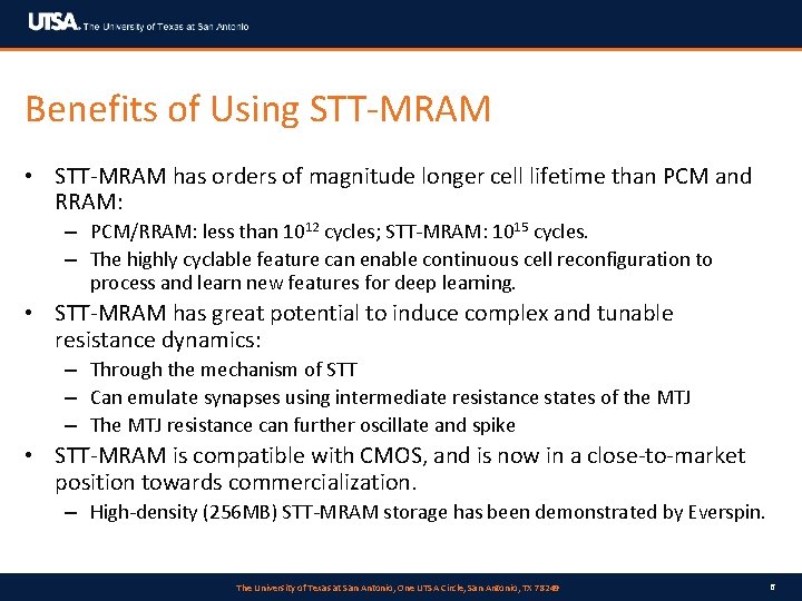
Benefits of Using STT-MRAM • STT-MRAM has orders of magnitude longer cell lifetime than PCM and RRAM: – PCM/RRAM: less than 1012 cycles; STT-MRAM: 1015 cycles. – The highly cyclable feature can enable continuous cell reconfiguration to process and learn new features for deep learning. • STT-MRAM has great potential to induce complex and tunable resistance dynamics: – Through the mechanism of STT – Can emulate synapses using intermediate resistance states of the MTJ – The MTJ resistance can further oscillate and spike • STT-MRAM is compatible with CMOS, and is now in a close-to-market position towards commercialization. – High-density (256 MB) STT-MRAM storage has been demonstrated by Everspin. The University of Texas at San Antonio, One UTSA Circle, San Antonio, TX 78249 6

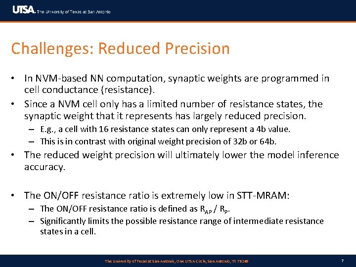
Challenges: Reduced Precision • In NVM-based NN computation, synaptic weights are programmed in cell conductance (resistance). • Since a NVM cell only has a limited number of resistance states, the synaptic weight that it represents has largely reduced precision. – E. g. , a cell with 16 resistance states can only represent a 4 b value. – This is in contrast with original weight precision of 32 b or 64 b. • The reduced weight precision will ultimately lower the model inference accuracy. • The ON/OFF resistance ratio is extremely low in STT-MRAM: – The ON/OFF resistance ratio is defined as RAP / RP. – Significantly limits the possible resistance range of intermediate resistance states in a cell. The University of Texas at San Antonio, One UTSA Circle, San Antonio, TX 78249 7

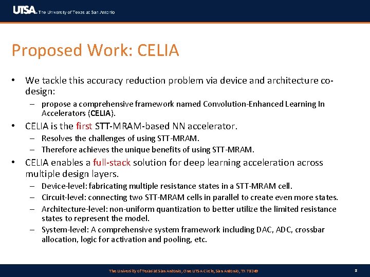
Proposed Work: CELIA • We tackle this accuracy reduction problem via device and architecture codesign: – propose a comprehensive framework named Convolution-Enhanced Learning In Accelerators (CELIA). • CELIA is the first STT-MRAM-based NN accelerator. – Resolves the challenges of using STT-MRAM. – Therefore achieves the unique benefits of using STT-MRAM. • CELIA enables a full-stack solution for deep learning acceleration across multiple design layers. – Device-level: fabricating multiple resistance states in a STT-MRAM cell. – Circuit-level: connecting two STT-MRAM cells in parallel to create even more states. – Architecture-level: non-uniform quantization to better utilize the limited resistance states to represent the model. – System-level: A comprehensive system framework including DAC, ADC, crossbar allocation, logic for activation and pooling, etc. The University of Texas at San Antonio, One UTSA Circle, San Antonio, TX 78249 8

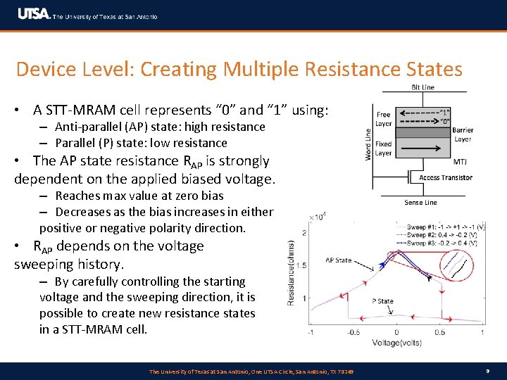
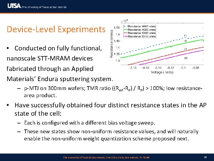
Device Level: Creating Multiple Resistance States • A STT-MRAM cell represents “ 0” and “ 1” using: – Anti-parallel (AP) state: high resistance – Parallel (P) state: low resistance • The AP state resistance RAP is strongly dependent on the applied biased voltage. – Reaches max value at zero bias – Decreases as the bias increases in either positive or negative polarity direction. • RAP depends on the voltage sweeping history. – By carefully controlling the starting voltage and the sweeping direction, it is possible to create new resistance states in a STT-MRAM cell. The University of Texas at San Antonio, One UTSA Circle, San Antonio, TX 78249 9

Device-Level Experiments • Conducted on fully functional, nanoscale STT-MRAM devices fabricated through an Applied Materials’ Endura sputtering system. – p-MTJ on 300 mm wafers; TMR ratio ((RAP-RP) / RP) > 100%; low resistancearea product. • Have successfully obtained four distinct resistance states in the AP state of the cell: – Each is configured with a different bias voltage sweep. – These new states show non-uniform resistance values, and will naturally enable the non-uniform weight quantization scheme proposed next. The University of Texas at San Antonio, One UTSA Circle, San Antonio, TX 78249 10

Architecture Level: Non-Uniform Weight Quantization • Using the intermediate resistance states provided by the device level, synaptic weights are programmed into STT-MRAM cell conductance. • Still results in model accuracy loss, due to the limited cell resistance states. • Our architecture-level work seeks to better utilize these resistances to represent the original model: – Identifies the most important weight quantization points in a non-uniform manner. The University of Texas at San Antonio, One UTSA Circle, San Antonio, TX 78249 11

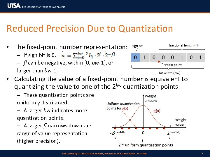
Reduced Precision Due to Quantization • The fixed-point number representation: – If sign bit is 0, – fl can be negative, within [0, bw-1], or larger than bw-1. • Calculating the value of a fixed-point number is equivalent to quantizing the value to one of the 2 bw quantization points. – These quantization points are uniformly distributed. – A larger bw indicates more quantization points. – A larger fl narrows down the range of value representation (higher precision). The University of Texas at San Antonio, One UTSA Circle, San Antonio, TX 78249 12

Non-Uniform Quantization • The most important quantization points are NOT uniformly distributed: – A quantization point that is close to zero has minimal impact on the model accuracy because of the low weight value it represents. – A quantization point that is far from zero also shows limited impact because only a very small amount of weights are quantized to it. The University of Texas at San Antonio, One UTSA Circle, San Antonio, TX 78249 13

Ineffectiveness of Existing Schemes • Uniform quantization: – Static: uses fixed integer and fractional lengths for the whole model. – Dynamic: allows tuning the fractional length across different layers (but the generated quantization points are still uniform). • Non-uniform quantization: – Log. Net [ICASSP 17]: • The first point is at 1/2 of the max weight value, and each additional point is at the mid-point between zero and the previous point. • Relies on a fixed quantization function (unaware of the weight distribution) • Simply assigns more quantization points towards zero. – SPINDLE [ISLPED 14]: similar to Log. Net but uses tanh(). – Deep Compression [ICLR 16]: • Groups synaptic weights and assigns quantization points learned from data. • Involves expensive model re-training; requires a lookup table. The University of Texas at San Antonio, One UTSA Circle, San Antonio, TX 78249 14

Proposed Solution • We construct an importance function g(x)*|x| to approximate the importance of different quantization points to the model inference accuracy. – It takes into account both the weight value and the weight amount. – The most important quantization points are around the peaks. • To quantify these quantization points: – Evenly partition the area between the function curve and the x-axis into a few regions. – The quantization point is the x-axis value that divides the region into halves (analogous to the center of mass for this region). The University of Texas at San Antonio, One UTSA Circle, San Antonio, TX 78249 15

Proposed Solution (Cont. ) • Furthermore, we generalize the importance function to be g(x)*|x|k, so that the weight value can be prioritized differently by adjusting k. • We test different values of k in the range of [0, 2] with a stride of 0. 1, and pick the one that gives the highest model accuracy. The University of Texas at San Antonio, One UTSA Circle, San Antonio, TX 78249 16

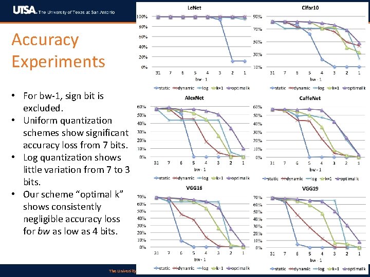
Accuracy Experiments • For bw-1, sign bit is excluded. • Uniform quantization schemes show significant accuracy loss from 7 bits. • Log quantization shows little variation from 7 to 3 bits. • Our scheme “optimal k” shows consistently negligible accuracy loss for bw as low as 4 bits. The University of Texas at San Antonio, One UTSA Circle, San Antonio, TX 78249 17

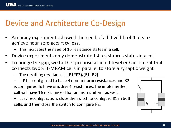
Device and Architecture Co-Design • Accuracy experiments showed the need of a bit width of 4 bits to achieve near-zero accuracy loss. – This indicates the need of 16 resistance states in a cell. • Device experiments only demonstrated 4 resistances states in a cell. • To bridge the gap, we further propose a circuit-level enhancement that connects two STT-MRAM cells in parallel to store a synaptic weight. – The resulting resistance is (R 1*R 2)/(R 1+R 2). – If R 1 is configured to have 4 non-uniform resistances and R 2 is configured to have another 4 resistances, the implemented cell will have 16 resistances that are non-uniform as well. – Easy reconfiguration: close the switch to configure R 1 in both cells, and then close the switch to configure R 2. The University of Texas at San Antonio, One UTSA Circle, San Antonio, TX 78249 18

System Level: An Accelerator System Design • The accelerator system is composed of a number of compute units (CU) connected to on-chip buffers and global buses. Organization is similar to PRIME [ISCA 16] and Pipe. Layer [HPCA 17]. • Synaptic weights are programmed in the crossbar arrays; inputs are fetched from memory chips to buffers, then enter the CU pipeline. • Each CU processes data in a pipelined manner. The University of Texas at San Antonio, One UTSA Circle, San Antonio, TX 78249 19

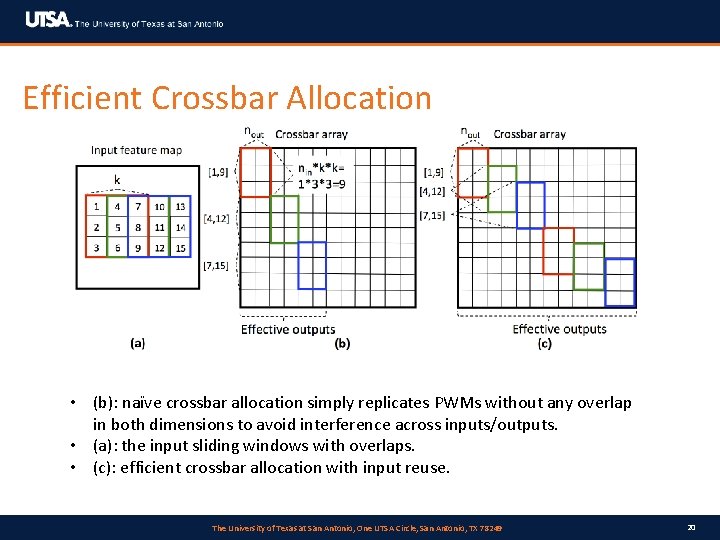
Efficient Crossbar Allocation • (b): naïve crossbar allocation simply replicates PWMs without any overlap in both dimensions to avoid interference across inputs/outputs. • (a): the input sliding windows with overlaps. • (c): efficient crossbar allocation with input reuse. The University of Texas at San Antonio, One UTSA Circle, San Antonio, TX 78249 20

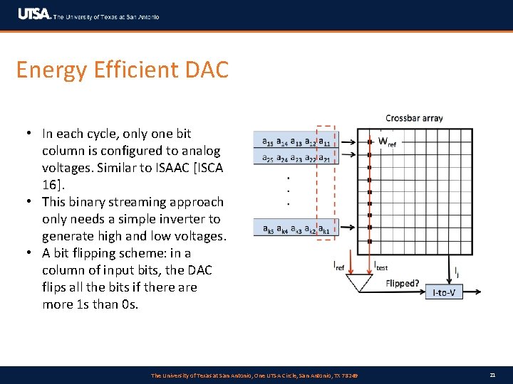
Energy Efficient DAC • In each cycle, only one bit column is configured to analog voltages. Similar to ISAAC [ISCA 16]. • This binary streaming approach only needs a simple inverter to generate high and low voltages. • A bit flipping scheme: in a column of input bits, the DAC flips all the bits if there are more 1 s than 0 s. The University of Texas at San Antonio, One UTSA Circle, San Antonio, TX 78249 21

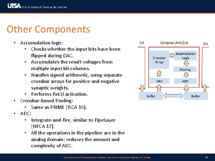
Other Components • Accumulation logic: • Checks whether the input bits have been flipped during DAC. • Accumulates the result voltages from multiple input bit columns. • Handles signed arithmetic, using separate crossbar arrays for positive and negative synaptic weights. • Performs Re. LU activation. • Crossbar-based Pooling: • Same as PRIME [ISCA 16]. • ADC: • Integrate-and-fire, similar to Pipe. Layer [HPCA 17]. • All the operations in the pipeline are in the analog domain; reduces the amount and complexity of ADC. The University of Texas at San Antonio, One UTSA Circle, San Antonio, TX 78249 22

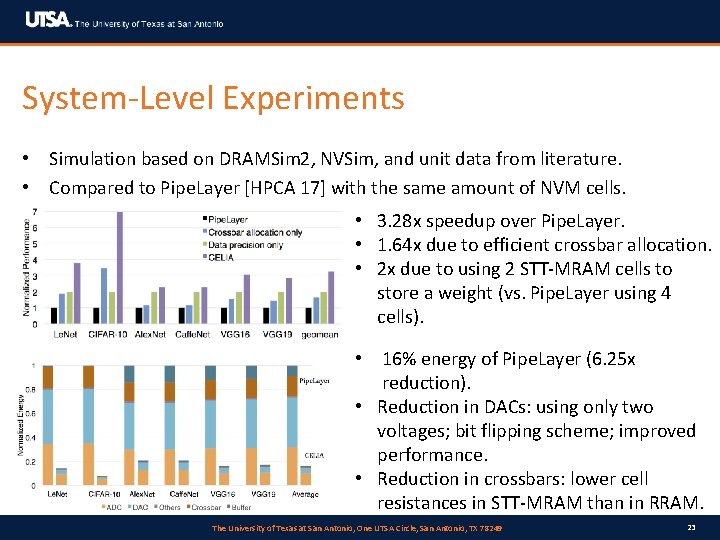
System-Level Experiments • Simulation based on DRAMSim 2, NVSim, and unit data from literature. • Compared to Pipe. Layer [HPCA 17] with the same amount of NVM cells. • 3. 28 x speedup over Pipe. Layer. • 1. 64 x due to efficient crossbar allocation. • 2 x due to using 2 STT-MRAM cells to store a weight (vs. Pipe. Layer using 4 cells). • 16% energy of Pipe. Layer (6. 25 x reduction). • Reduction in DACs: using only two voltages; bit flipping scheme; improved performance. • Reduction in crossbars: lower cell resistances in STT-MRAM than in RRAM. The University of Texas at San Antonio, One UTSA Circle, San Antonio, TX 78249 23

Summary • CELIA enables NVM-based deep learning acceleration. • CELIA is the first STT-MRAM-based NN accelerator. – Resolves the challenges of using STT-MRAM. – Therefore achieves the unique benefits of using STT-MRAM. • CELIA enables a full-stack solution for deep learning acceleration across multiple design layers. – Device-level: fabricating multiple resistance states in a STT-MRAM cell. – Circuit-level: connecting two STT-MRAM cells in parallel to create even more states. – Architecture-level: non-uniform quantization to better utilize the limited resistance states to represent the model. – System-level: A comprehensive system framework including DAC, ADC, crossbar allocation, logic for activation and pooling, etc. The University of Texas at San Antonio, One UTSA Circle, San Antonio, TX 78249 24

Thanks! Q&A. The University of Texas at San Antonio, One UTSA Circle, San Antonio, TX 78249

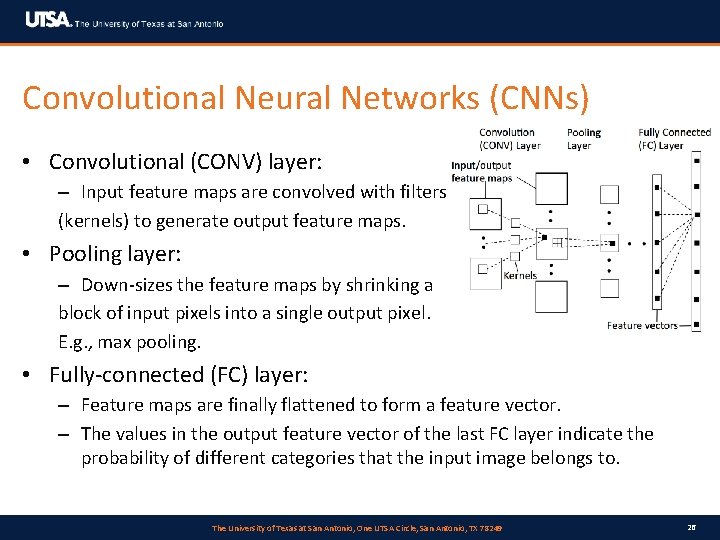
Convolutional Neural Networks (CNNs) • Convolutional (CONV) layer: – Input feature maps are convolved with filters (kernels) to generate output feature maps. • Pooling layer: – Down-sizes the feature maps by shrinking a block of input pixels into a single output pixel. E. g. , max pooling. • Fully-connected (FC) layer: – Feature maps are finally flattened to form a feature vector. – The values in the output feature vector of the last FC layer indicate the probability of different categories that the input image belongs to. The University of Texas at San Antonio, One UTSA Circle, San Antonio, TX 78249 26

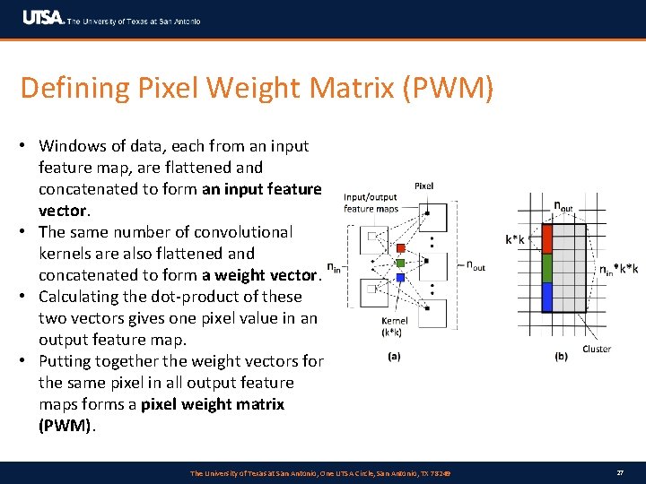
Defining Pixel Weight Matrix (PWM) • Windows of data, each from an input feature map, are flattened and concatenated to form an input feature vector. • The same number of convolutional kernels are also flattened and concatenated to form a weight vector. • Calculating the dot-product of these two vectors gives one pixel value in an output feature map. • Putting together the weight vectors for the same pixel in all output feature maps forms a pixel weight matrix (PWM). The University of Texas at San Antonio, One UTSA Circle, San Antonio, TX 78249 27