CCU 25 Communication and Control Unit ASIC in
![CCU 25 Block diagram Interrupts[0 -3]* JTAG Master ST 1 ST 2 ST 3 CCU 25 Block diagram Interrupts[0 -3]* JTAG Master ST 1 ST 2 ST 3](https://slidetodoc.com/presentation_image_h2/b19ae005af05691fd023951c7563b689/image-8.jpg)
- Slides: 19

CCU 25 Communication and Control Unit ASIC in CMOS 0. 25 μm Ch. Paillard LECC 2002 COLMAR Ch. Paillard CERN EP 1

SUMMARY • • CMS tracker slow control Network architecture and redundancy Messages structure CCU 25 Bloc diagram Detail of Blocs I 2 C, parallel, memory, jtag, trigger Radiation hardness and irradiation test Conclusions LECC 2002 COLMAR Ch. Paillard CERN EP 2

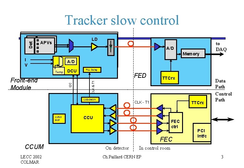
Det Tracker slow control LD APVs A/D Memory I V A/D I 2 C Front-end Module DCU PLL-Delay FED LVDSMUX LVDS BUF TTCrx CLK & T 1 Temp CLK - T 1 TTCrx CCU FEC ctrl FEC CCUM LECC 2002 COLMAR to DAQ On detector Data Path Control Path PCI Intfc In control room Ch. Paillard CERN EP 3

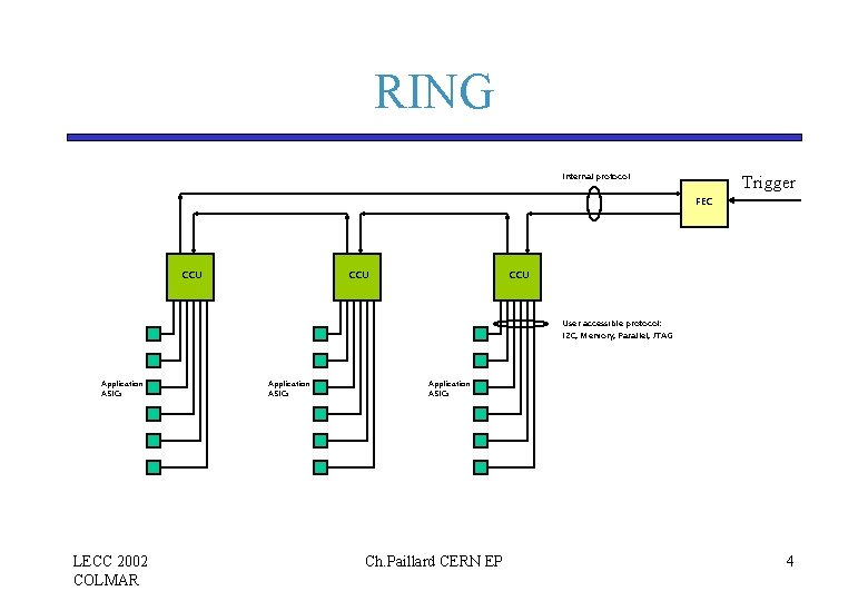
RING Internal protocol Trigger FEC CCU CCU User accessible protocol: I 2 C, Memory, Parallel, JTAG Application ASICs LECC 2002 COLMAR Application ASICs Ch. Paillard CERN EP 4

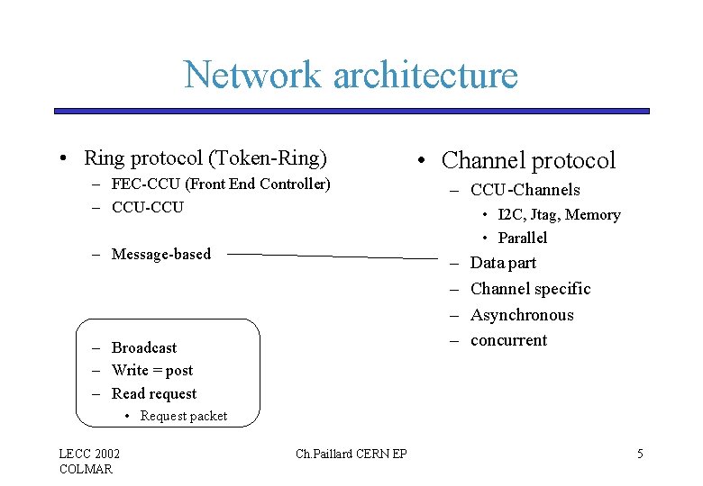
Network architecture • Ring protocol (Token-Ring) • Channel protocol – FEC-CCU (Front End Controller) – CCU-CCU – CCU-Channels – Message-based – – – Broadcast – Write = post – Read request • I 2 C, Jtag, Memory • Parallel Data part Channel specific Asynchronous concurrent • Request packet LECC 2002 COLMAR Ch. Paillard CERN EP 5

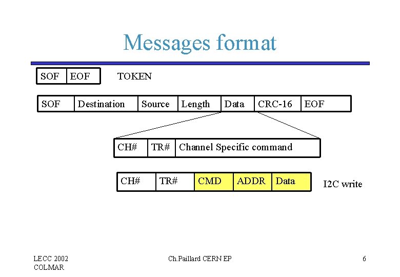
Messages format SOF EOF TOKEN Destination CH# LECC 2002 COLMAR Source Length Data CRC-16 EOF TR# Channel Specific command TR# CMD Ch. Paillard CERN EP ADDR Data I 2 C write 6

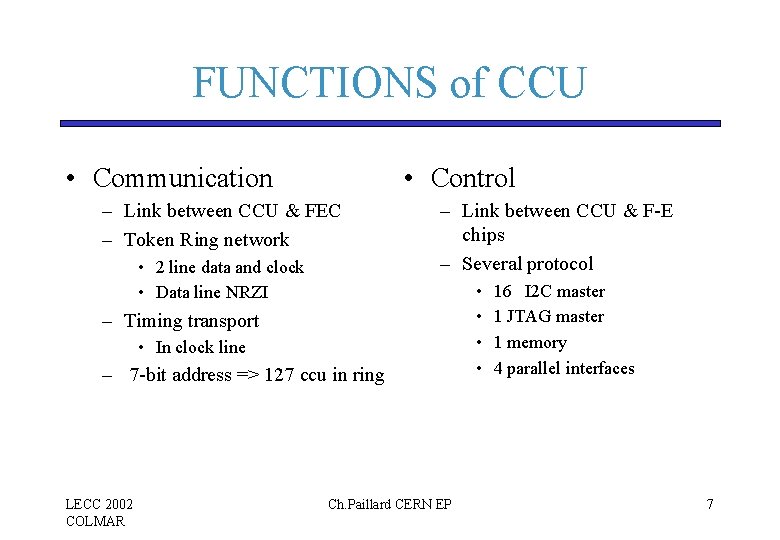
FUNCTIONS of CCU • Communication • Control – Link between CCU & FEC – Token Ring network • 2 line data and clock • Data line NRZI – Link between CCU & F-E chips – Several protocol – Timing transport • In clock line – 7 -bit address => 127 ccu in ring LECC 2002 COLMAR Ch. Paillard CERN EP • • 16 I 2 C master 1 JTAG master 1 memory 4 parallel interfaces 7
![CCU 25 Block diagram Interrupts0 3 JTAG Master ST 1 ST 2 ST 3 CCU 25 Block diagram Interrupts[0 -3]* JTAG Master ST 1 ST 2 ST 3](https://slidetodoc.com/presentation_image_h2/b19ae005af05691fd023951c7563b689/image-8.jpg)
CCU 25 Block diagram Interrupts[0 -3]* JTAG Master ST 1 ST 2 ST 3 ST 4 Trigger Decoder JTAG Slave Clock Distribution Link Controller Node Controller SCL SDATA CLKI(A) CLKI(B) CLKO(A) DO(A) Trigger Counter & other timing logic Reset* 16 x I 2 C Buses Alarms I 2 C Master DI(A) CLKO(B) DI(B) Memory Bus Interface Parallel interface Ext Reset* I 2 C Master D[0: 7] A[0: 15] R/W CS[1 -2]* PA[0: 7] PB[0: 7] PC[0: 7] PD[0: 7] Local Bus LECC 2002 COLMAR Ch. Paillard CERN EP 8

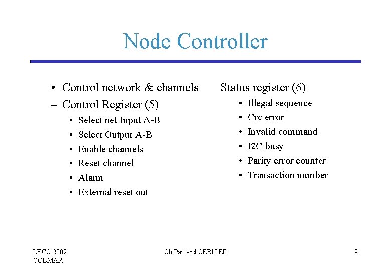
Node Controller • Control network & channels – Control Register (5) • • • LECC 2002 COLMAR Status register (6) Select net Input A-B Select Output A-B Enable channels Reset channel Alarm External reset out Ch. Paillard CERN EP • • • Illegal sequence Crc error Invalid command I 2 C busy Parity error counter Transaction number 9

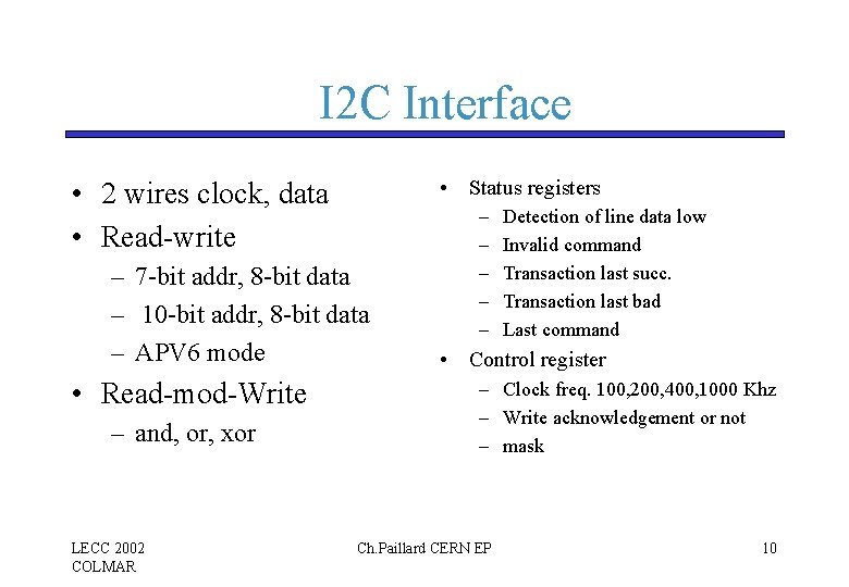
I 2 C Interface • Status registers • 2 wires clock, data • Read-write – 7 -bit addr, 8 -bit data – 10 -bit addr, 8 -bit data – APV 6 mode • Read-mod-Write – and, or, xor LECC 2002 COLMAR – – – Detection of line data low Invalid command Transaction last succ. Transaction last bad Last command • Control register – Clock freq. 100, 200, 400, 1000 Khz – Write acknowledgement or not – mask Ch. Paillard CERN EP 10

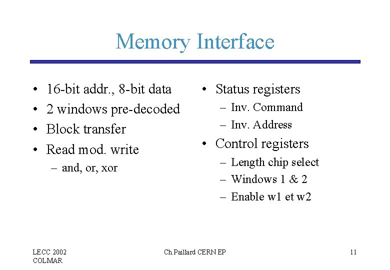
Memory Interface • • 16 -bit addr. , 8 -bit data 2 windows pre-decoded Block transfer Read mod. write – and, or, xor LECC 2002 COLMAR • Status registers – Inv. Command – Inv. Address • Control registers – Length chip select – Windows 1 & 2 – Enable w 1 et w 2 Ch. Paillard CERN EP 11

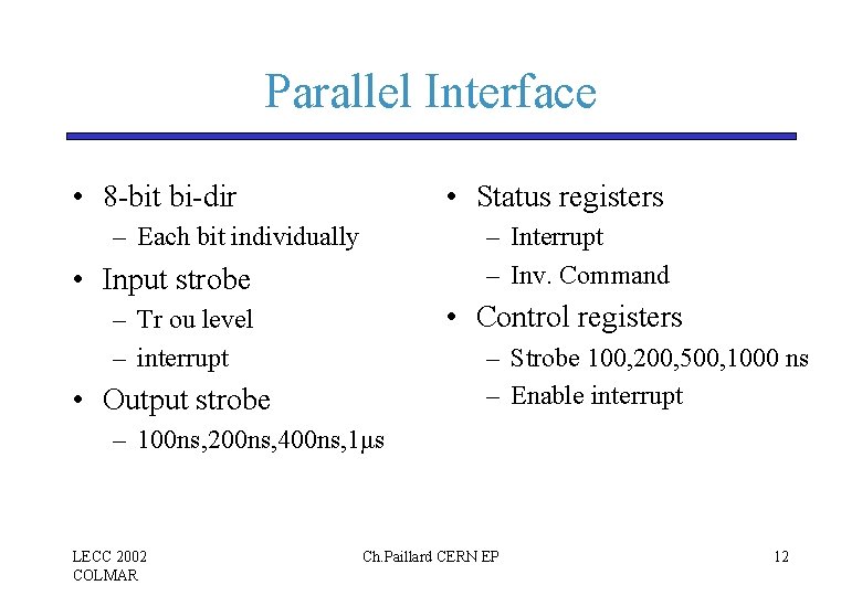
Parallel Interface • 8 -bit bi-dir • Status registers – Each bit individually – Interrupt – Inv. Command • Input strobe • Control registers – Tr ou level – interrupt – Strobe 100, 200, 500, 1000 ns – Enable interrupt • Output strobe – 100 ns, 200 ns, 400 ns, 1μs LECC 2002 COLMAR Ch. Paillard CERN EP 12

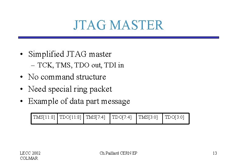
JTAG MASTER • Simplified JTAG master – TCK, TMS, TDO out, TDI in • No command structure • Need special ring packet • Example of data part message TMS[11: 8] TDO[11: 8] TMS[7: 4] LECC 2002 COLMAR TDO[7: 4] Ch. Paillard CERN EP TMS[3: 0] TDO[3: 0] 13

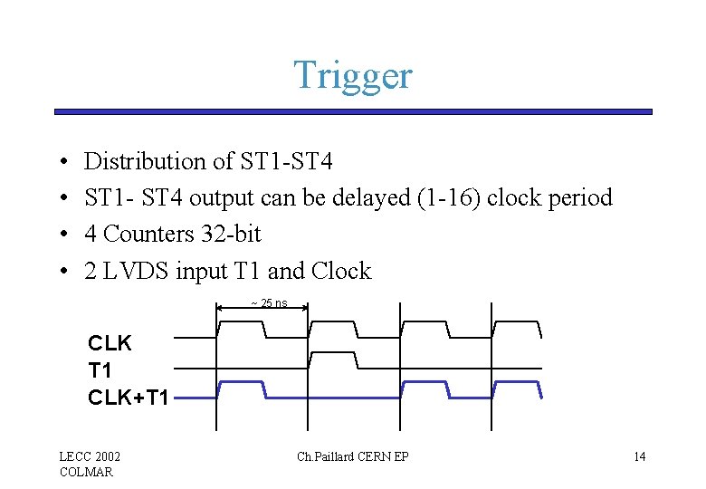
Trigger • • Distribution of ST 1 -ST 4 ST 1 - ST 4 output can be delayed (1 -16) clock period 4 Counters 32 -bit 2 LVDS input T 1 and Clock ~ 25 ns CLK T 1 CLK+T 1 LECC 2002 COLMAR Ch. Paillard CERN EP 14

Redundancy LECC 2002 COLMAR Ch. Paillard CERN EP 15

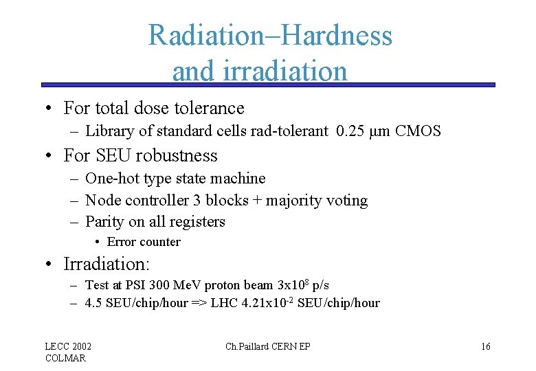
Radiation–Hardness and irradiation • For total dose tolerance – Library of standard cells rad-tolerant 0. 25 μm CMOS • For SEU robustness – One-hot type state machine – Node controller 3 blocks + majority voting – Parity on all registers • Error counter • Irradiation: – Test at PSI 300 Me. V proton beam 3 x 10⁸ p/s – 4. 5 SEU/chip/hour => LHC 4. 21 x 10 -2 SEU/chip/hour LECC 2002 COLMAR Ch. Paillard CERN EP 16

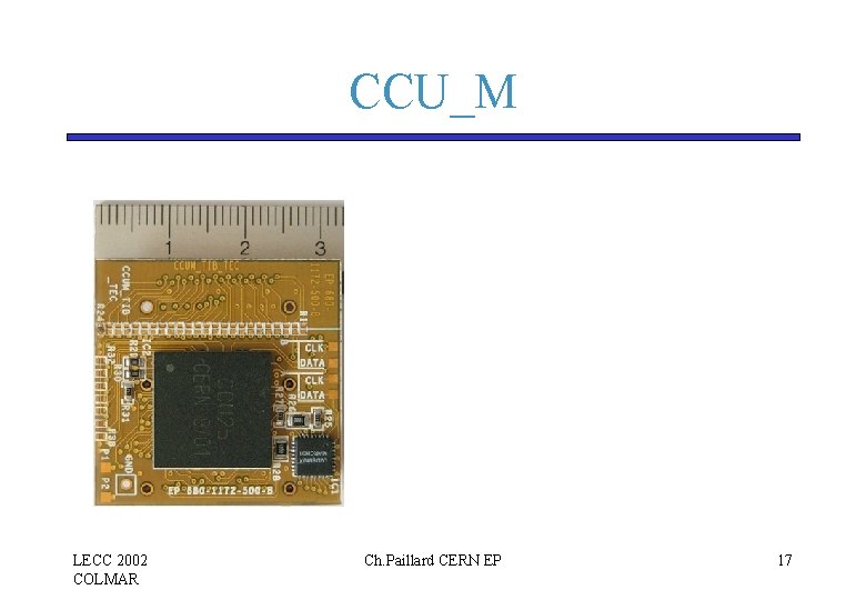
CCU_M photo LECC 2002 COLMAR Ch. Paillard CERN EP 17

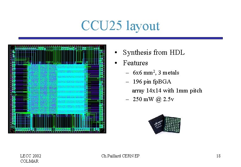
CCU 25 layout • Synthesis from HDL • Features – 6 x 6 mm 2, 3 metals – 196 pin fp. BGA array 14 x 14 with 1 mm pitch – 250 m. W @ 2. 5 v LECC 2002 COLMAR Ch. Paillard CERN EP 18

CONCLUSIONS • Network interface (Like Token Ring) 40 Mb/s • Control interface – I 2 C, parallel, memory bus and JTAG. • Radiation resistant LECC 2002 COLMAR Ch. Paillard CERN EP 19