Case Study SRAM Caches By Nikhil Suryanarayanan Outline

Case Study - SRAM & Caches By Nikhil Suryanarayanan

Outline • • • Introduction SRAM Cell Peripheral Circuitry Practical Cache Designs Technology scaling & Power Reduction Summary
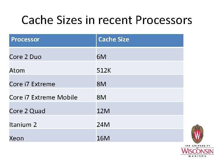
Cache Sizes in recent Processors Processor Cache Size Core 2 Duo 6 M Atom 512 K Core i 7 Extreme 8 M Core i 7 Extreme Mobile 8 M Core 2 Quad 12 M Itanium 2 24 M Xeon 16 M
SRAM Cell • Basic building block of on-chip cache • Various design 12 T, 10 T, 8 T, 6 T, 4 T • 6 T is the most widely used by industry giants in contemporary microprocessors • Data bit and its complement and stored in a cross-coupled inverter • Simple in design
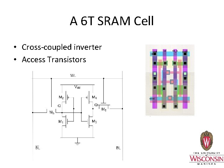
A 6 T SRAM Cell • Cross-coupled inverter • Access Transistors
Column Circuitry • Bitline Conditioning • Sense Amplifiers • Multiplexer (column decoder)
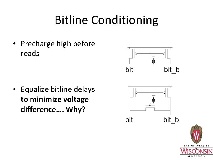
Bitline Conditioning • Precharge high before reads • Equalize bitline delays to minimize voltage difference…. Why?
Sense Amplifier • Bitlines have many cells attached; enormous capacitive loads • Bitlines swing slowly • Voltages equalized during precharge • SA detects small swing as bitlines are driven apart and bring it up to normal logic • Reduced delay by not waiting for full-swing
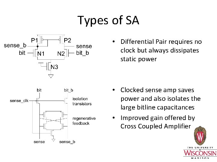
Types of SA • Differential Pair requires no clock but always dissipates static power • Clocked sense amp saves power and also isolates the large bitline capacitances • Improved gain offered by Cross Coupled Amplifier
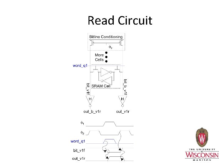
Read Circuit
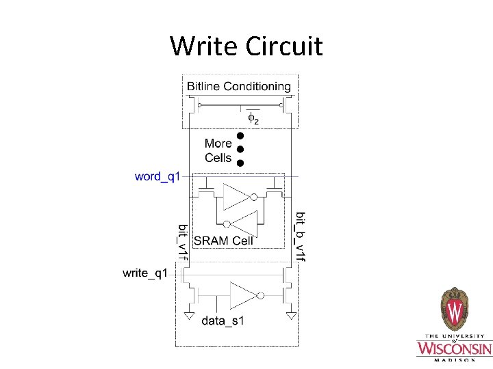
Write Circuit
Drive strengths • • • Read Stability Writeability NMOS pull down – Strongest Access NMOS – intermediate PMOS pull up - weakest
Industry Designs • Novel Design Techniques • Embedded Dual 512 KB L 2$ in Ultrasparc (2004) • L 1$, L 2$ & L 3$ - Designs in two Itanium Generations (2002 -2003) • Effects of Technology scaling • Overview of current Design in 45 nm
Design Considerations • Larger on-chip cache running at processor frequency improves performance • Latency also increases as size grows • Memory cell performance does not improve rapidly with new generation • Change of design focus with the cache level
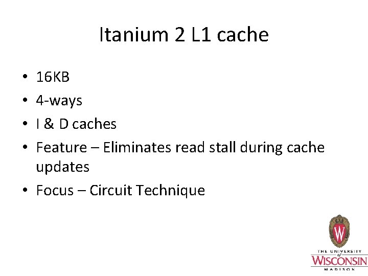
Itanium 2 L 1 cache 16 KB 4 -ways I & D caches Feature – Eliminates read stall during cache updates • Focus – Circuit Technique • •
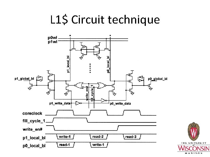
L 1$ Circuit technique
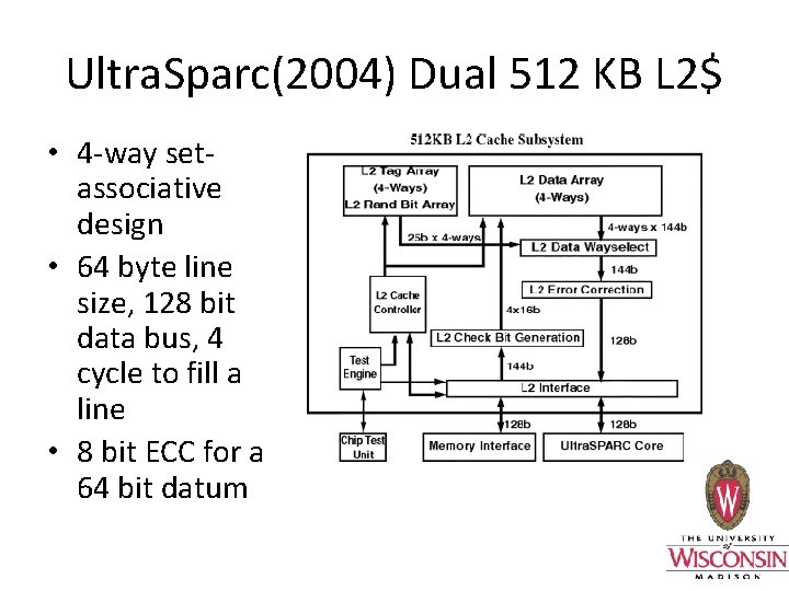
Ultra. Sparc(2004) Dual 512 KB L 2$ • 4 -way setassociative design • 64 byte line size, 128 bit data bus, 4 cycle to fill a line • 8 bit ECC for a 64 bit datum
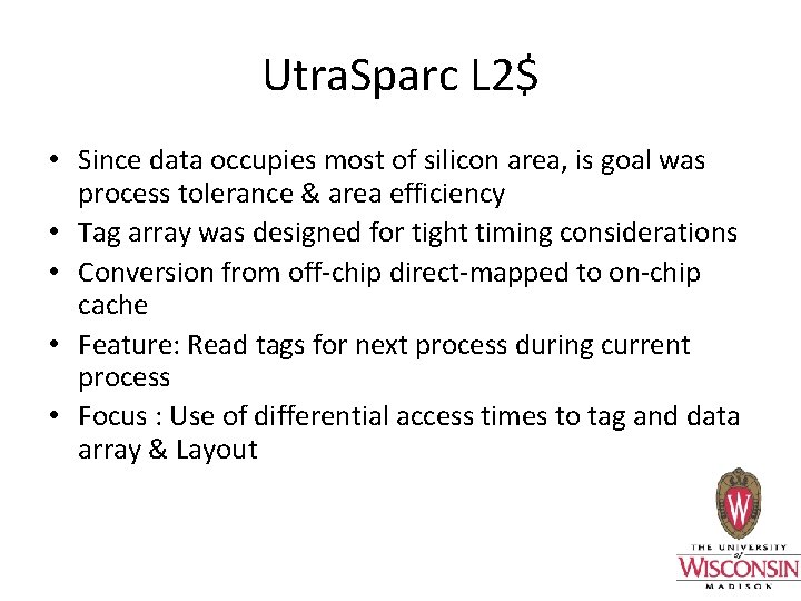
Utra. Sparc L 2$ • Since data occupies most of silicon area, is goal was process tolerance & area efficiency • Tag array was designed for tight timing considerations • Conversion from off-chip direct-mapped to on-chip cache • Feature: Read tags for next process during current process • Focus : Use of differential access times to tag and data array & Layout
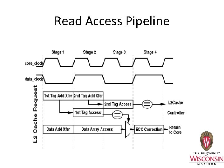
Read Access Pipeline
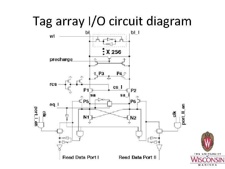
Tag array I/O circuit diagram
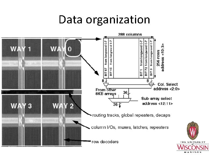
Data organization
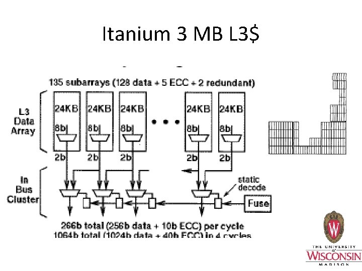
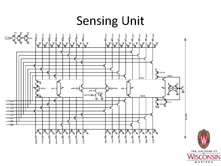
Itanium 3 MB L 3$ • • • 180 nm process 12 way set-associative Fits in an irregular structure Feature : Size of cache Focus : Regular & efficient partition in an irregular space
Itanium 3 MB L 3$
Sensing Unit
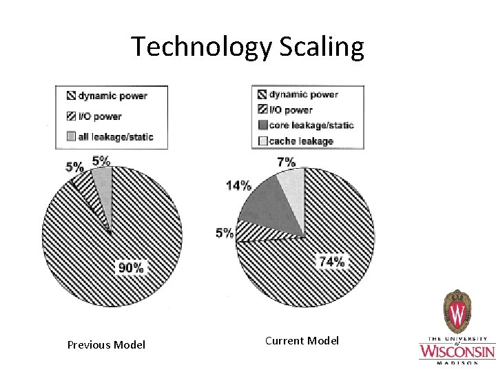
Itanium 2 6 MB L 3$ 24 -way set-associative 130 nm process 64 bit EPIC architecture processor Double the number of transistors compared to the previous generation • Same power dissipation as previous generation. . . hmmm • 1. 5 x freq, 2 x L 3 cache, 3. 5 x leakage • •
Technology Scaling Previous Model Current Model
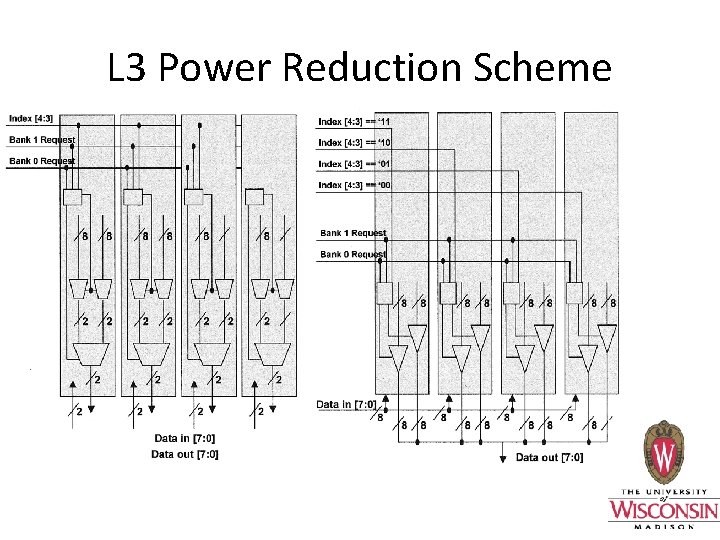
L 3 Power Reduction Scheme
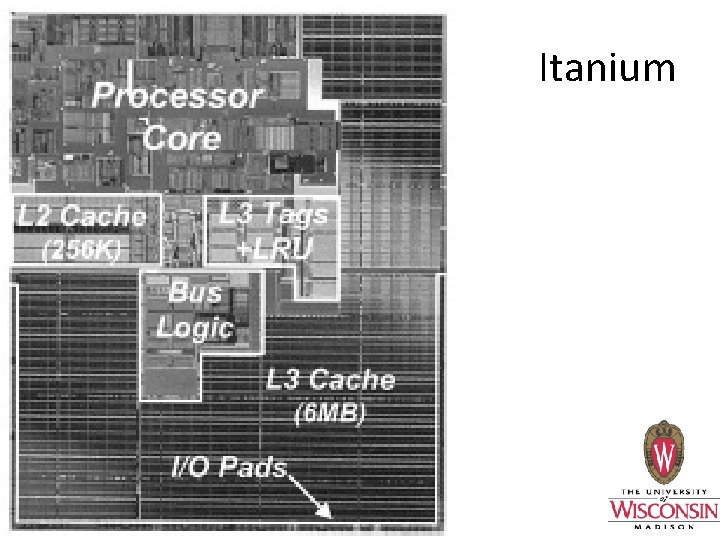
Itanium
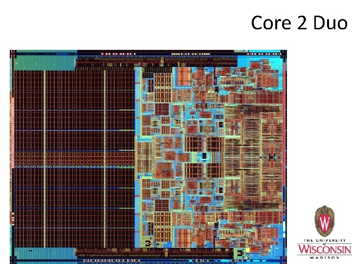
Core 2 Duo
Power Reduction techniques used in Silverthorne • Control registers disable a pair of ways(out of 8) during low performance operation • A way is entirely flushed before disablement • During Deep Power Down, the entire voltage plane to L 2 is cut off • General Cache Architecture has remained the same

Questions?
References • • CMOS VLSI Design, Weste & Harris 3 e On-Chip 3 MB Subarray based 3 rd level Cache on Itanium Microprocessor - Don Weiss, John J Wuu, Victor Chin Design and Implementation of an Embedded 512 KB Level-2 Cache Subsystem, Shin, Petrick, Singh, Leon A 1. 5 GHz 130 nm Itanium 2 Processor with 6 -MB On-die L 3 Cache
Need for Caches Large Access Delays of off-chip memory Fast on-chip Memory is expensive Hierarchical Memory System is a solution Bring limited amount of data on-chip and reduce latencies • Increase processor performance • •
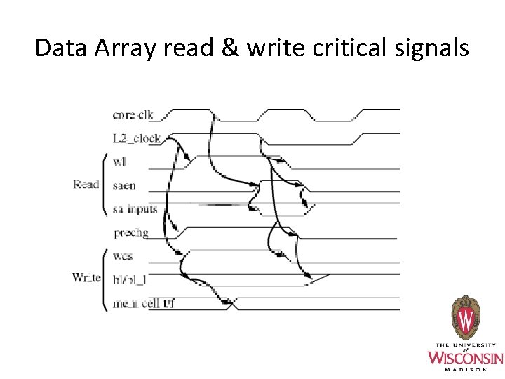
Data Array read & write critical signals
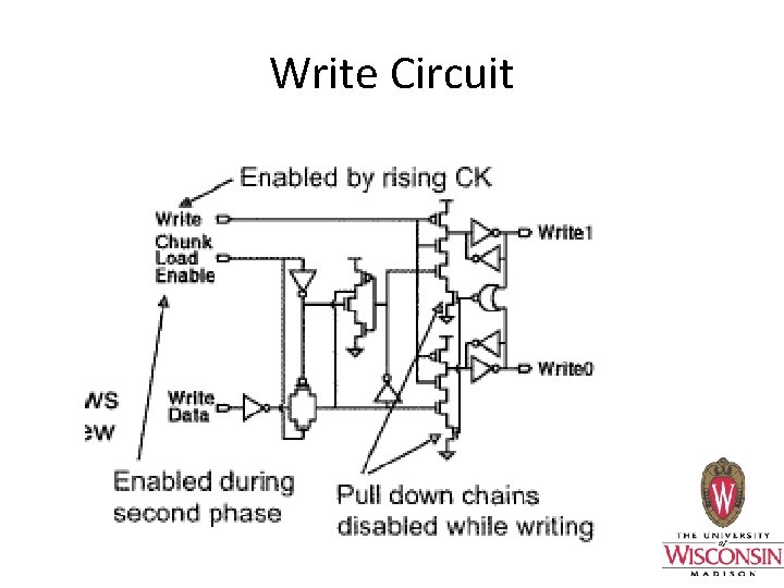
Write Circuit
- Slides: 35