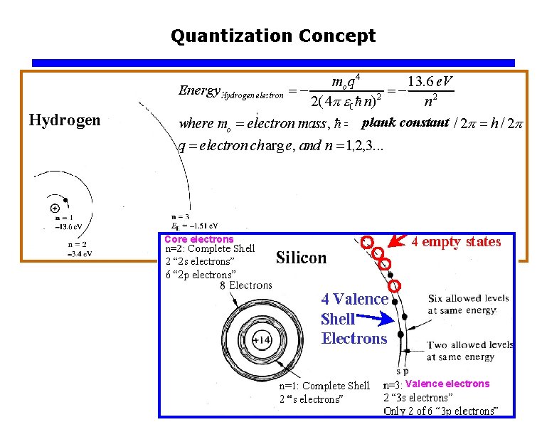
Carrier Modeling Quantization Concept plank constant Core electrons



- Slides: 67

Carrier Modeling

Quantization Concept plank constant Core electrons Valence electrons

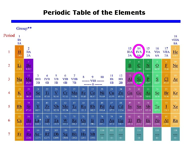
Periodic Table of the Elements

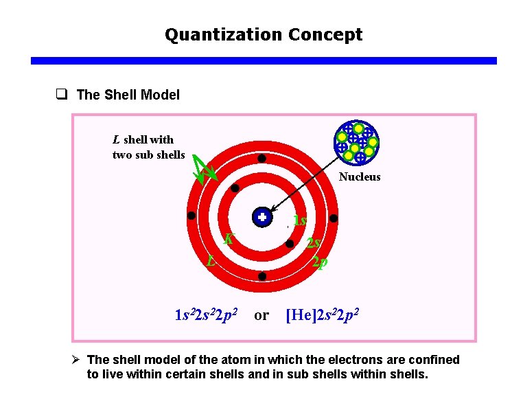
Quantization Concept q The Shell Model L shell with two sub shells Nucleus 1 s K L 1 s 22 p 2 or 2 s 2 p [He]2 s 22 p 2 Ø The shell model of the atom in which the electrons are confined to live within certain shells and in sub shells within shells.

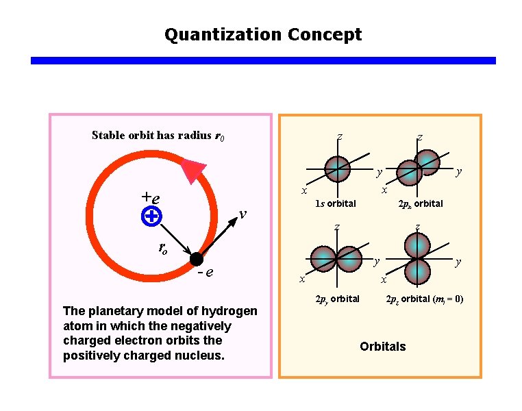
Quantization Concept Stable orbit has radius r 0 z v 1 s orbital 2 px orbital z z ro e The planetary model of hydrogen atom in which the negatively charged electron orbits the positively charged nucleus. y y x x +e z y x 2 py orbital 2 pz orbital (ml = 0) Orbitals

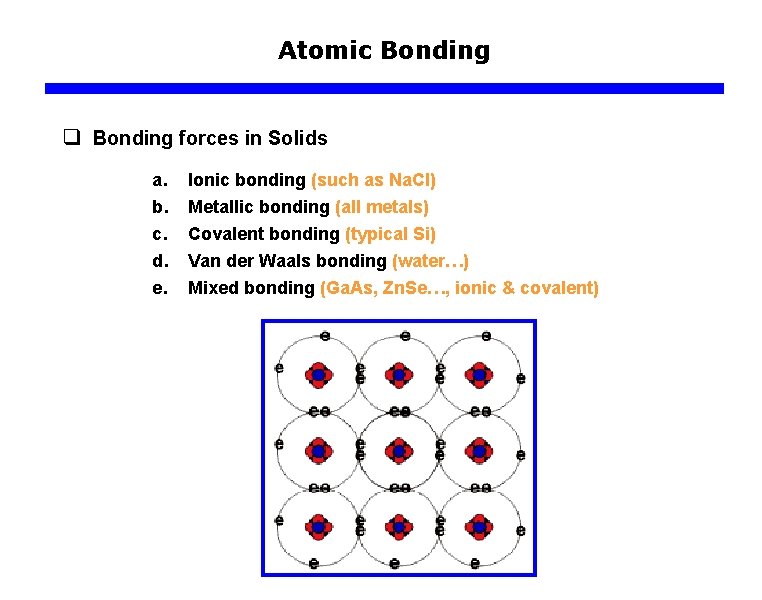
Atomic Bonding q Bonding forces in Solids a. b. c. d. e. Ionic bonding (such as Na. Cl) Metallic bonding (all metals) Covalent bonding (typical Si) Van der Waals bonding (water…) Mixed bonding (Ga. As, Zn. Se…, ionic & covalent)

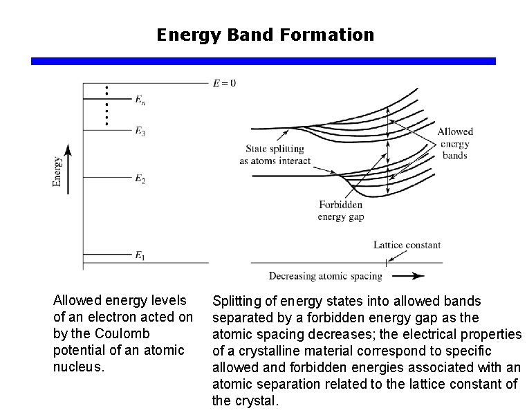
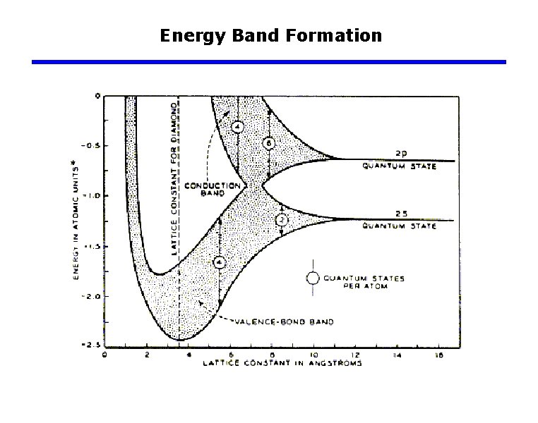
Energy Band Formation Allowed energy levels of an electron acted on by the Coulomb potential of an atomic nucleus. Splitting of energy states into allowed bands separated by a forbidden energy gap as the atomic spacing decreases; the electrical properties of a crystalline material correspond to specific allowed and forbidden energies associated with an atomic separation related to the lattice constant of the crystal.

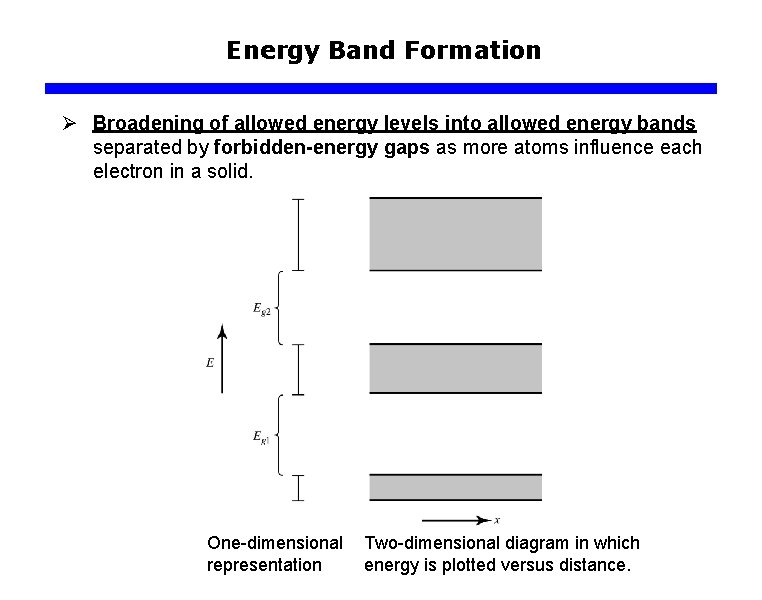
Energy Band Formation Ø Broadening of allowed energy levels into allowed energy bands separated by forbidden-energy gaps as more atoms influence each electron in a solid. One-dimensional representation Two-dimensional diagram in which energy is plotted versus distance.

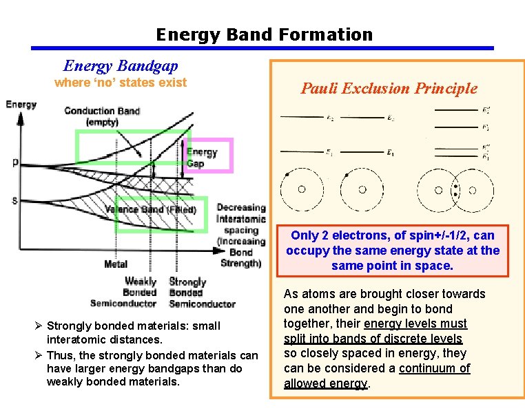
Energy Band Formation Energy Bandgap where ‘no’ states exist Pauli Exclusion Principle Only 2 electrons, of spin+/-1/2, can occupy the same energy state at the same point in space. Ø Strongly bonded materials: small interatomic distances. Ø Thus, the strongly bonded materials can have larger energy bandgaps than do weakly bonded materials. As atoms are brought closer towards one another and begin to bond together, their energy levels must split into bands of discrete levels so closely spaced in energy, they can be considered a continuum of allowed energy.

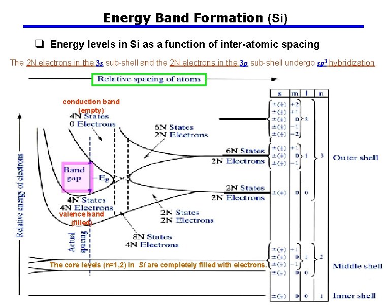
Energy Band Formation (Si) q Energy levels in Si as a function of inter-atomic spacing The 2 N electrons in the 3 s sub-shell and the 2 N electrons in the 3 p sub-shell undergo sp 3 hybridization. conduction band (empty) valence band (filled) The core levels (n=1, 2) in Si are completely filled with electrons.

Energy Band Formation

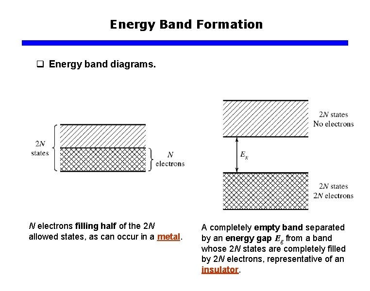
Energy Band Formation q Energy band diagrams. N electrons filling half of the 2 N allowed states, as can occur in a metal. A completely empty band separated by an energy gap Eg from a band whose 2 N states are completely filled by 2 N electrons, representative of an insulator.

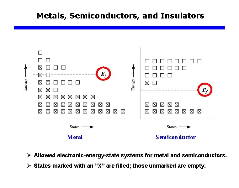
Metals, Semiconductors, and Insulators Ef Ef Metal Semiconductor Ø Allowed electronic-energy-state systems for metal and semiconductors. Ø States marked with an “X” are filled; those unmarked are empty.

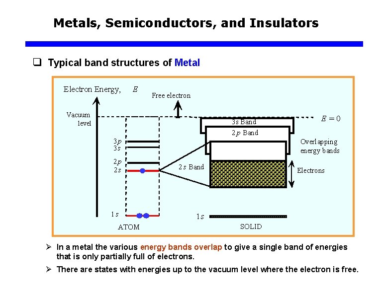
Metals, Semiconductors, and Insulators q Typical band structures of Metal Electron Energy, E Free electron Vacuum level 3 s Band E =0 2 p Band 3 p 3 s 2 p 2 s 1 s ATOM Overlapping energy bands 2 s Band Electrons 1 s SOLID Ø In a metal the various energy bands overlap to give a single band of energies that is only partially full of electrons. Ø There are states with energies up to the vacuum level where the electron is free.

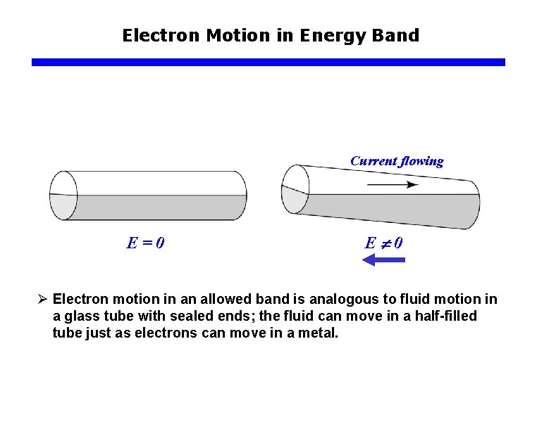
Electron Motion in Energy Band Current flowing E=0 E 0 Ø Electron motion in an allowed band is analogous to fluid motion in a glass tube with sealed ends; the fluid can move in a half-filled tube just as electrons can move in a metal.

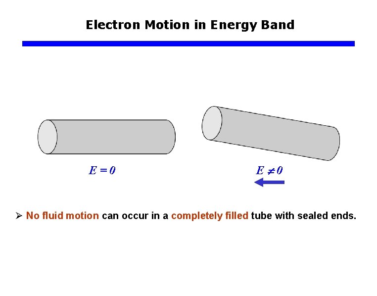
Electron Motion in Energy Band E=0 E 0 Ø No fluid motion can occur in a completely filled tube with sealed ends.

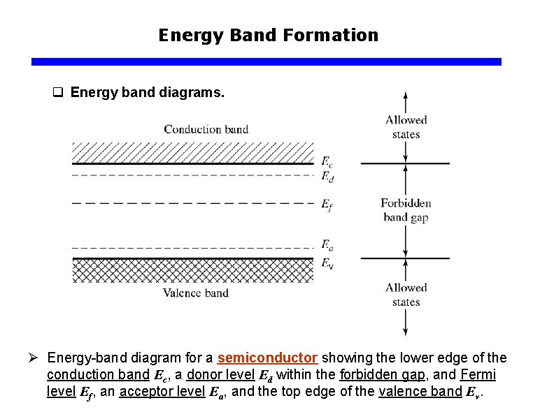
Energy Band Formation q Energy band diagrams. Ø Energy-band diagram for a semiconductor showing the lower edge of the conduction band Ec, a donor level Ed within the forbidden gap, and Fermi level Ef, an acceptor level Ea, and the top edge of the valence band Ev.

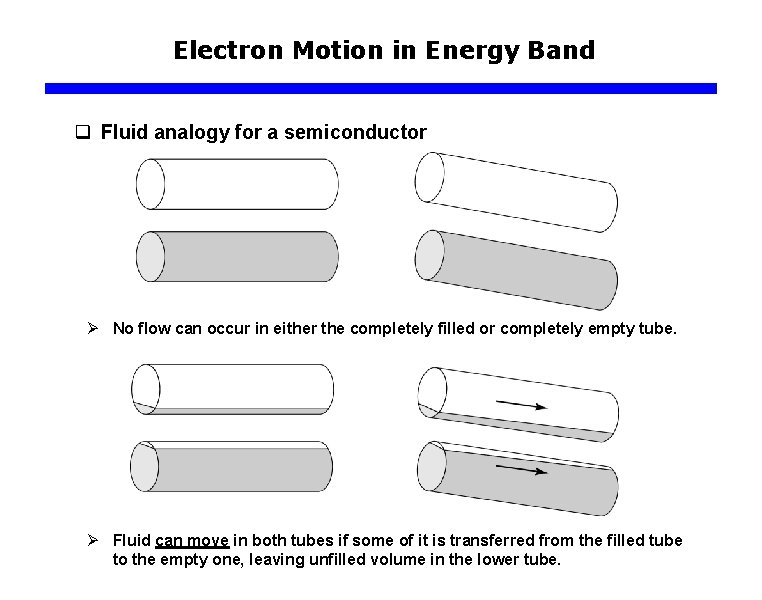
Electron Motion in Energy Band q Fluid analogy for a semiconductor Ø No flow can occur in either the completely filled or completely empty tube. Ø Fluid can move in both tubes if some of it is transferred from the filled tube to the empty one, leaving unfilled volume in the lower tube.

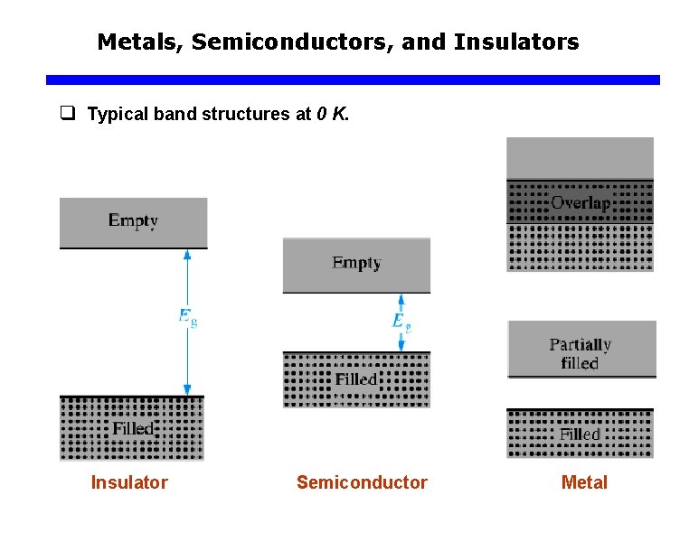
Metals, Semiconductors, and Insulators q Typical band structures at 0 K. Insulator Semiconductor Metal

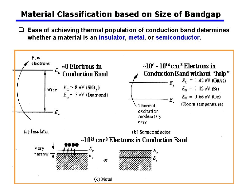
Material Classification based on Size of Bandgap q Ease of achieving thermal population of conduction band determines whether a material is an insulator, metal, or semiconductor.

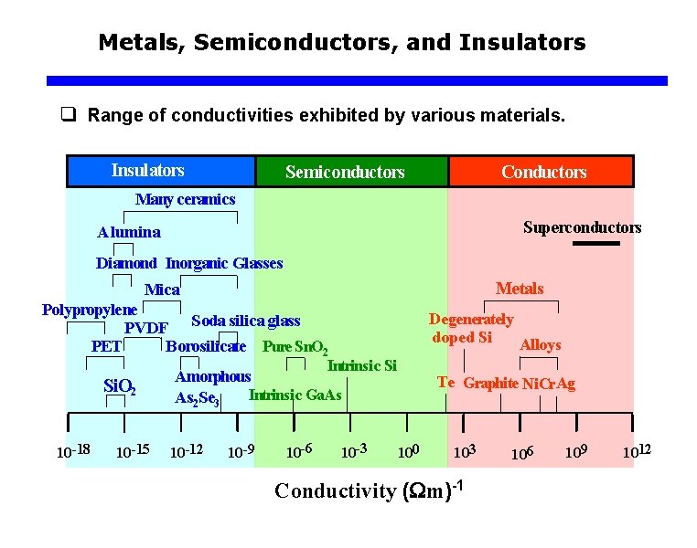
Metals, Semiconductors, and Insulators q Range of conductivities exhibited by various materials. Insulators Semiconductors Conductors Many ceramics Superconductors Alumina Diamond Inorganic Glasses Metals Mica Polypropylene PVDF Soda silica glass Borosilicate Pure Sn. O 2 PET Si. O 2 10 -18 10 -15 Degenerately doped Si Alloys Intrinsic Si Amorphous Intrinsic Ga. As As 2 Se 3 10 -12 10 -9 10 -6 10 -3 Te Graphite Ni. Cr. Ag 100 103 Conductivity ( m)-1 106 109 1012

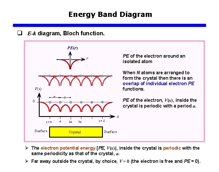
Energy Band Diagram q E-k diagram, Bloch function. PE(r) PE of the electron around an isolated atom r When N atoms are arranged to form the crystal then there is an overlap of individual electron PE functions. V(x) a a 0 PE of the electron, V(x), inside the crystal is periodic with a period a. x x=0 Surface a 2 a 3 a Crystal x=L Surface Ø The electron potential energy [PE, V(x)], inside the crystal is periodic with the same periodicity as that of the crystal, a. Ø Far away outside the crystal, by choice, V = 0 (the electron is free and PE = 0).

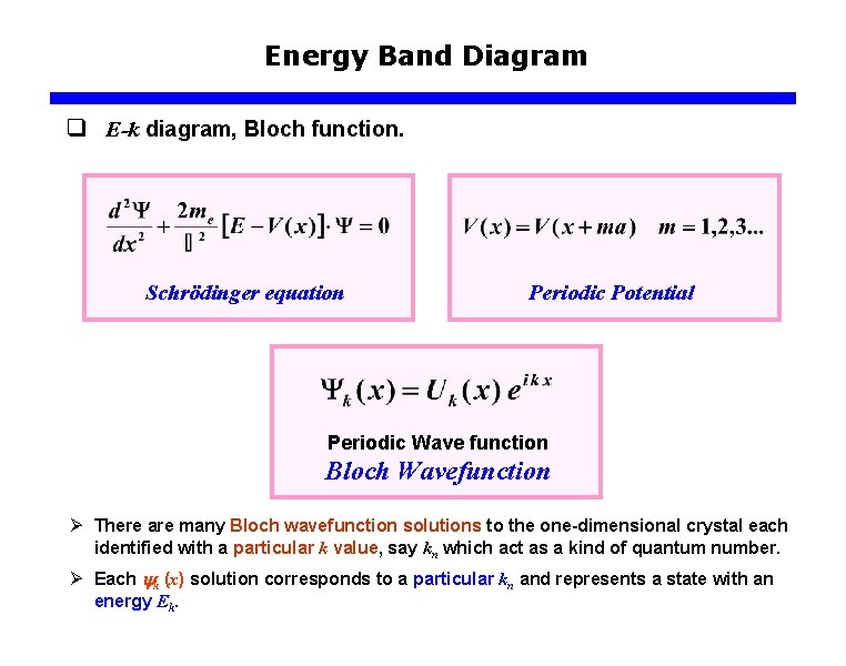
Energy Band Diagram q E-k diagram, Bloch function. Schrödinger equation Periodic Potential Periodic Wave function Bloch Wavefunction Ø There are many Bloch wavefunction solutions to the one-dimensional crystal each identified with a particular k value, say kn which act as a kind of quantum number. Ø Each k (x) solution corresponds to a particular kn and represents a state with an energy Ek.

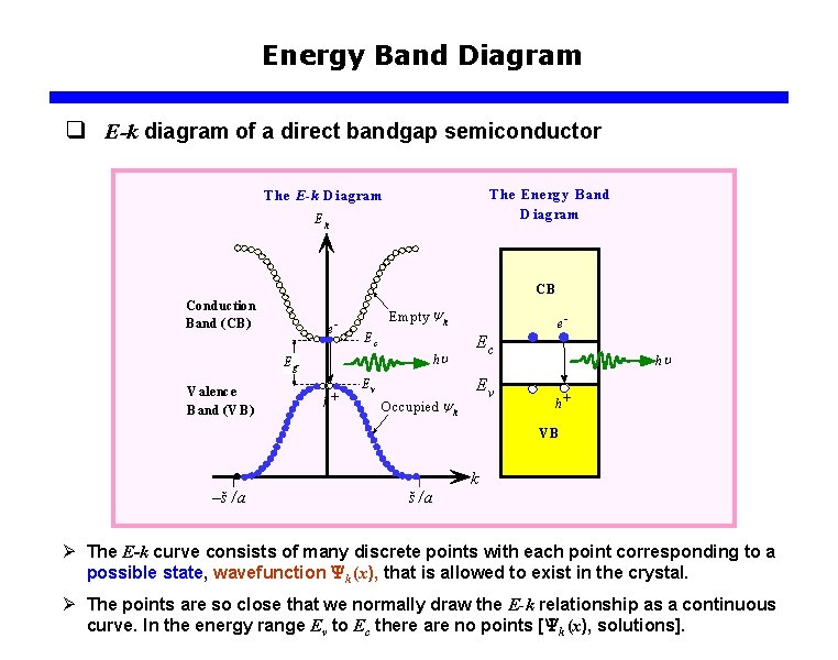
Energy Band Diagram q E-k diagram of a direct bandgap semiconductor The Energ y B and D iag ram The E-k D iag ram Ek CB Conduction B and (CB ) e Em pty y k Ec Eg V alence B and (V B ) h+ hu Ev O ccupied y k e Ec Ev hu h+ VB k –š /a Ø The E-k curve consists of many discrete points with each point corresponding to a possible state, wavefunction k (x), that is allowed to exist in the crystal. Ø The points are so close that we normally draw the E-k relationship as a continuous curve. In the energy range Ev to Ec there are no points [ k (x), solutions].

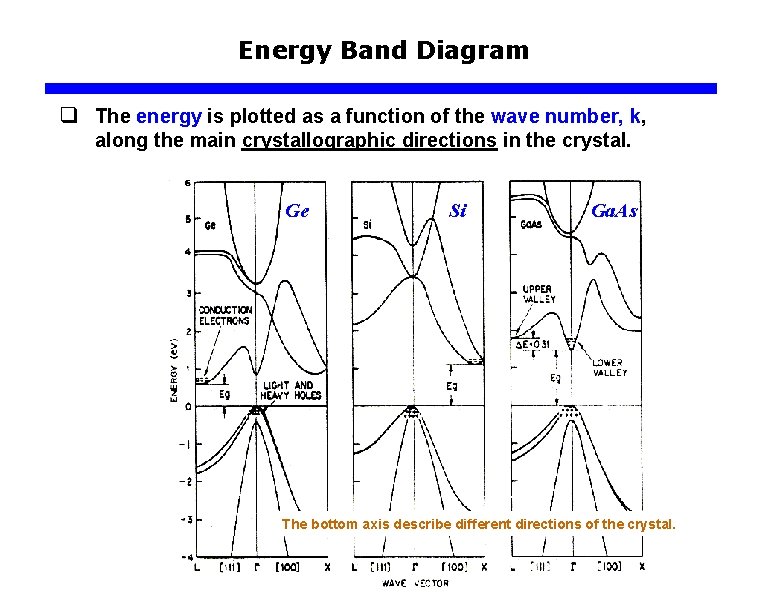
Energy Band Diagram q The energy is plotted as a function of the wave number, k, along the main crystallographic directions in the crystal. Ge Si Ga. As The bottom axis describe different directions of the crystal.

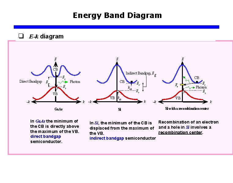
Energy Band Diagram q E-k diagram E E E CB Direct Bandgap Ec Eg Indirect Bandgap, Eg Photon CB Ev kcb VB k –k Ga. As In Ga. As the minimum of the CB is directly above the maximum of the VB. direct bandgap semiconductor. –k VB kvb Si Ec CB Er Ev k –k Ec Phonon Ev VB k Si with a recombination center In Si, the minimum of the CB is Recombination of an electron displaced from the maximum of and a hole in Si involves a recombination center. the VB. indirect bandgap semiconductor

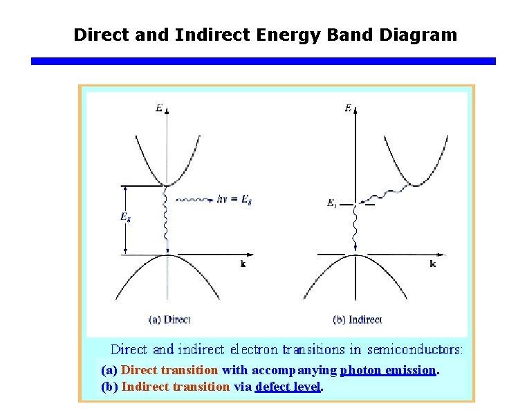
Direct and Indirect Energy Band Diagram (a) Direct transition with accompanying photon emission. (b) Indirect transition via defect level.

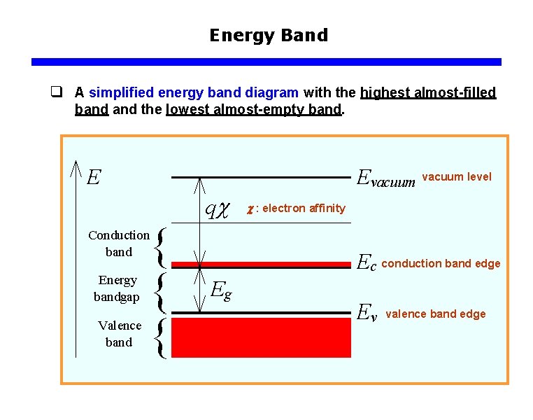
Energy Band q A simplified energy band diagram with the highest almost-filled band the lowest almost-empty band. vacuum level : electron affinity conduction band edge valence band edge

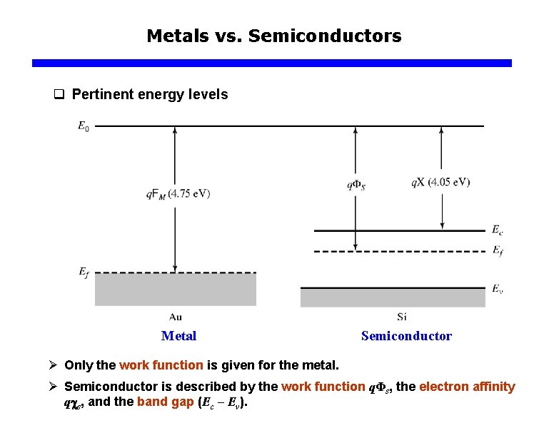
Metals vs. Semiconductors q Pertinent energy levels Metal Semiconductor Ø Only the work function is given for the metal. Ø Semiconductor is described by the work function qΦs, the electron affinity q s, and the band gap (Ec – Ev).

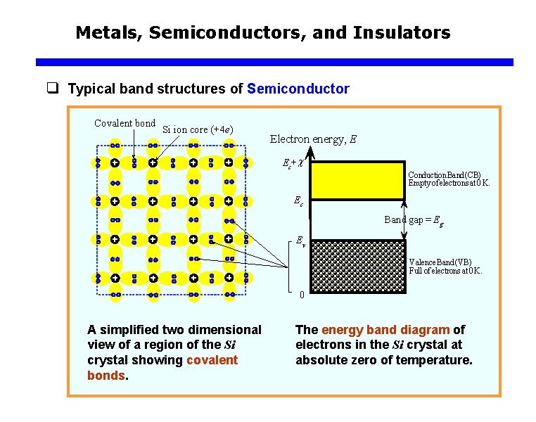
Metals, Semiconductors, and Insulators q Typical band structures of Semiconductor Covalent bond Si ion core (+4 e) Electron energy, E Ec+c Conduction Band (CB) Empty of electrons at 0 K. Ec Band gap = Eg Ev Valence Band (VB) Full of electrons at 0 K. 0 A simplified two dimensional view of a region of the Si crystal showing covalent bonds. The energy band diagram of electrons in the Si crystal at absolute zero of temperature.

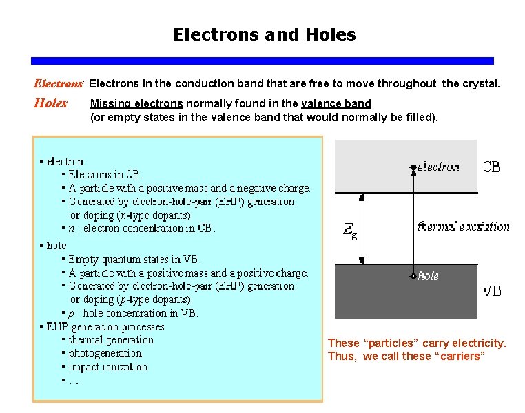
Electrons and Holes Electrons: Electrons in the conduction band that are free to move throughout the crystal. Holes: Missing electrons normally found in the valence band (or empty states in the valence band that would normally be filled). These “particles” carry electricity. Thus, we call these “carriers”

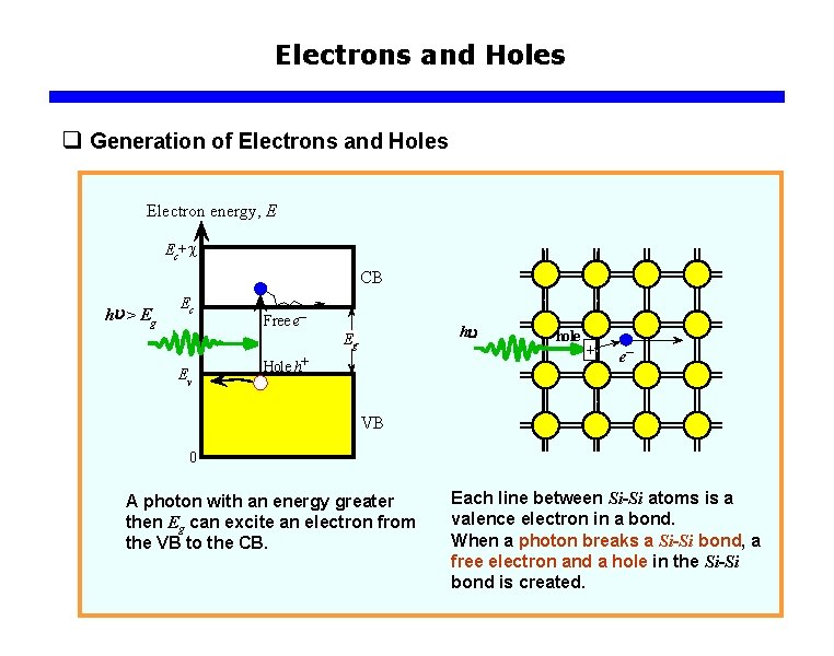
Electrons and Holes q Generation of Electrons and Holes Electron energy, E Ec+c CB hu > Eg Ec Free e– hu Eg Ev Hole h+ hole e– VB 0 A photon with an energy greater then Eg can excite an electron from the VB to the CB. Each line between Si-Si atoms is a valence electron in a bond. When a photon breaks a Si-Si bond, a free electron and a hole in the Si-Si bond is created.

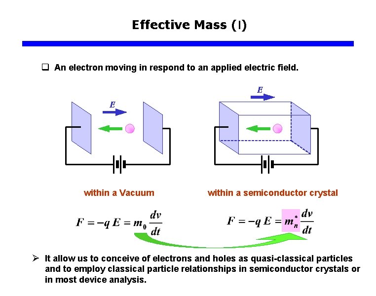
Effective Mass (I) q An electron moving in respond to an applied electric field. E E within a Vacuum within a semiconductor crystal Ø It allow us to conceive of electrons and holes as quasi-classical particles and to employ classical particle relationships in semiconductor crystals or in most device analysis.

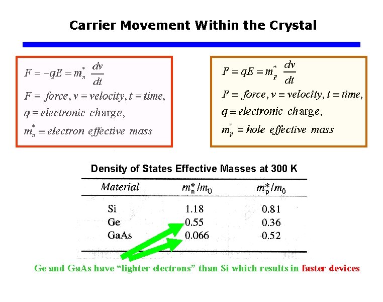
Carrier Movement Within the Crystal Density of States Effective Masses at 300 K Ge and Ga. As have “lighter electrons” than Si which results in faster devices

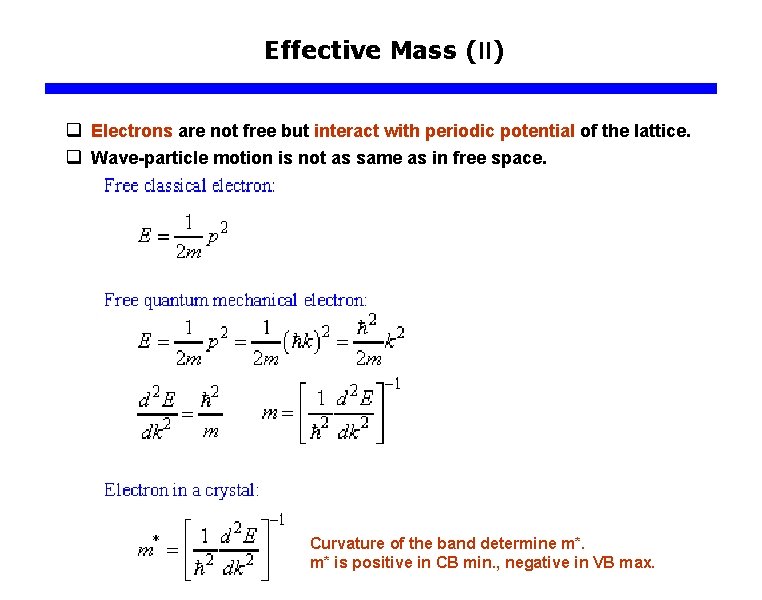
Effective Mass (II) q Electrons are not free but interact with periodic potential of the lattice. q Wave-particle motion is not as same as in free space. Curvature of the band determine m*. m* is positive in CB min. , negative in VB max.

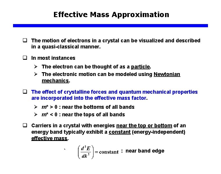
Effective Mass Approximation q The motion of electrons in a crystal can be visualized and described in a quasi-classical manner. q In most instances Ø The electron can be thought of as a particle. Ø The electronic motion can be modeled using Newtonian mechanics. q The effect of crystalline forces and quantum mechanical properties are incorporated into the effective mass factor. Ø m* > 0 : near the bottoms of all bands Ø m* < 0 : near the tops of all bands q Carriers in a crystal with energies near the top or bottom of an energy band typically exhibit a constant (energy-independent) effective mass. ` : near band edge

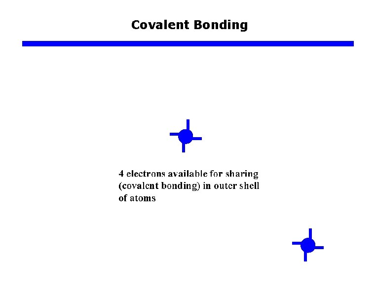
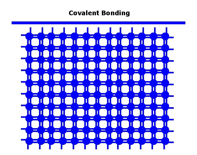
Covalent Bonding

Covalent Bonding

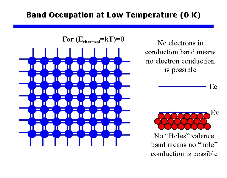
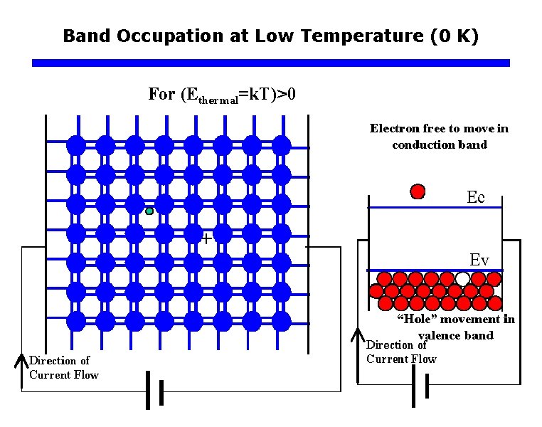
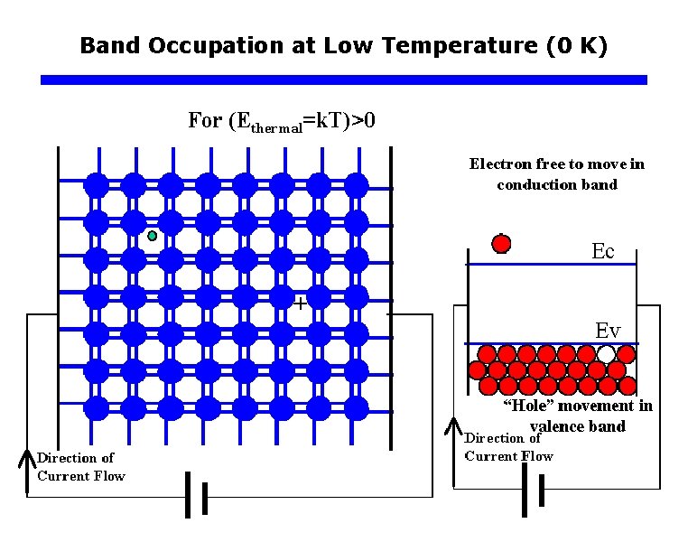
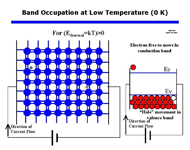
Band Occupation at Low Temperature (0 K)

Band Occupation at Low Temperature (0 K)

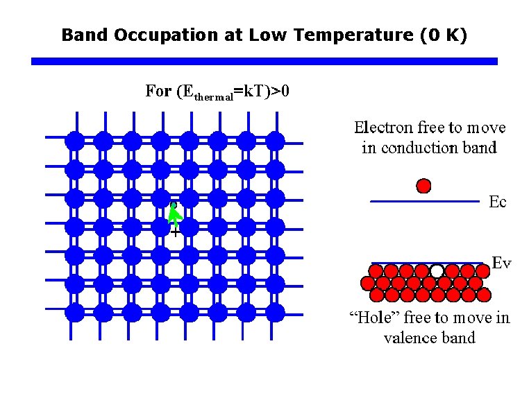
Band Occupation at Low Temperature (0 K)

Band Occupation at Low Temperature (0 K)

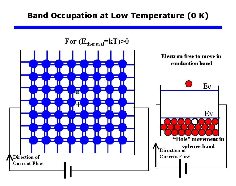
Band Occupation at Low Temperature (0 K)

Band Occupation at Low Temperature (0 K)

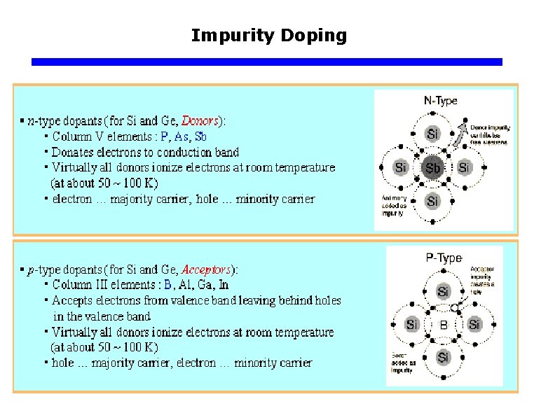
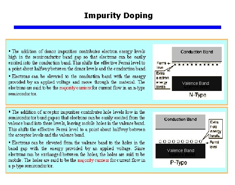
Impurity Doping q The need for more control over carrier concentration Ø Without “help” the total number of “carriers” (electrons and holes) is limited to 2 ni. Ø For most materials, this is not that much, and leads to very high resistance and few useful applications. Ø We need to add carriers by modifying the crystal. Ø This process is known as “doping the crystal”.

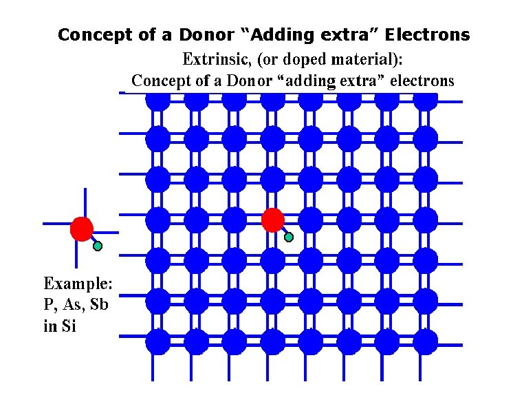
Concept of a Donor “Adding extra” Electrons

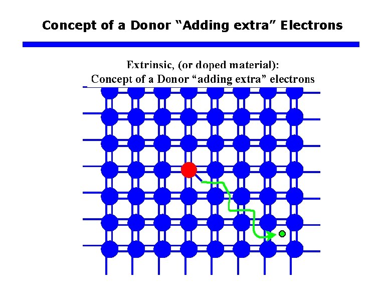
Concept of a Donor “Adding extra” Electrons

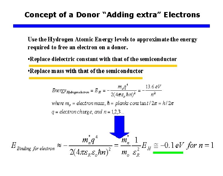
Concept of a Donor “Adding extra” Electrons

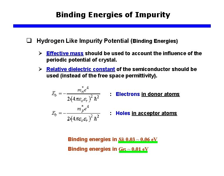
Binding Energies of Impurity q Hydrogen Like Impurity Potential (Binding Energies) Ø Effective mass should be used to account the influence of the periodic potential of crystal. Ø Relative dielectric constant of the semiconductor should be used (instead of the free space permittivity). : Electrons in donor atoms : Holes in acceptor atoms Binding energies in Si: 0. 03 ~ 0. 06 e. V Binding energies in Ge: ~ 0. 01 e. V

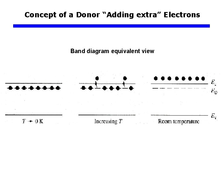
Concept of a Donor “Adding extra” Electrons Band diagram equivalent view

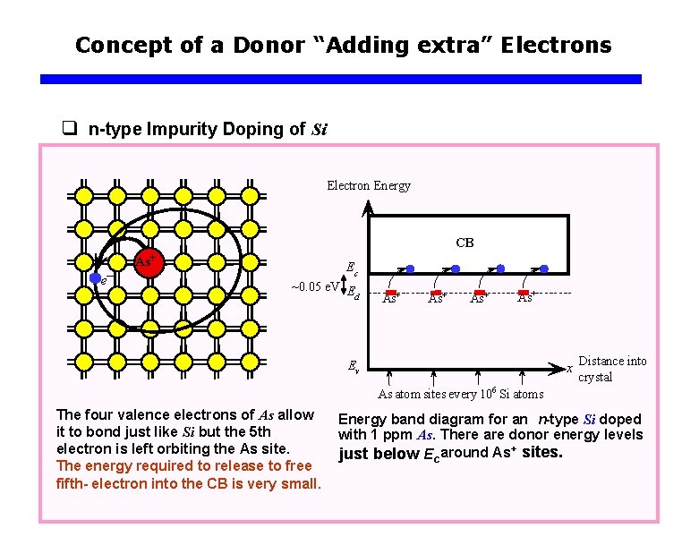
Concept of a Donor “Adding extra” Electrons q n-type Impurity Doping of Si Electron Energy CB e– As+ Ec ~0. 05 e. V E d As+ As+ Ev x Distance into crystal As atom sites every 106 Si atoms The four valence electrons of As allow it to bond just like Si but the 5 th electron is left orbiting the As site. The energy required to release to free fifth- electron into the CB is very small. Energy band diagram for an n-type Si doped with 1 ppm As. There are donor energy levels just below Ec around As+ sites.

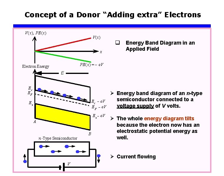
Concept of a Donor “Adding extra” Electrons V(x), PE (x) V(x) x q Energy Band Diagram in an Applied Field PE (x) = – e. V Electron Energy E Ec EF E c - e. V E F - e. V Ev E v - e. V A n Type Semiconductor B Ø Energy band diagram of an n-type semiconductor connected to a voltage supply of V volts. Ø The whole energy diagram tilts because the electron now has an electrostatic potential energy as well. Ø Current flowing V

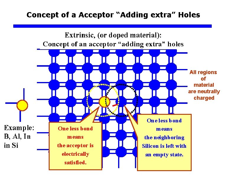
Concept of a Acceptor “Adding extra” Holes All regions of material are neutrally charged One less bond means the acceptor is electrically satisfied. One less bond means the neighboring Silicon is left with an empty state.

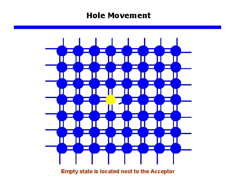
Hole Movement Empty state is located next to the Acceptor

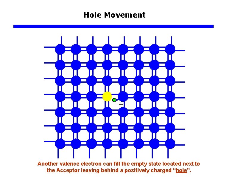
Hole Movement Another valence electron can fill the empty state located next to the Acceptor leaving behind a positively charged “hole”.

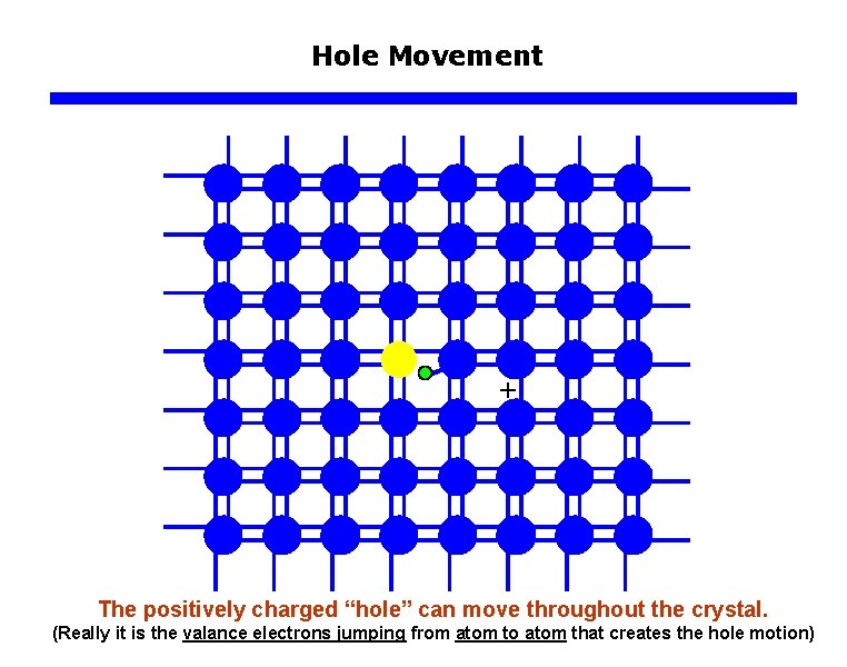
Hole Movement The positively charged “hole” can move throughout the crystal. (Really it is the valance electrons jumping from atom to atom that creates the hole motion)

Hole Movement The positively charged “hole” can move throughout the crystal. (Really it is the valance electrons jumping from atom to atom that creates the hole motion)

Hole Movement The positively charged “hole” can move throughout the crystal. (Really it is the valance electrons jumping from atom to atom that creates the hole motion)

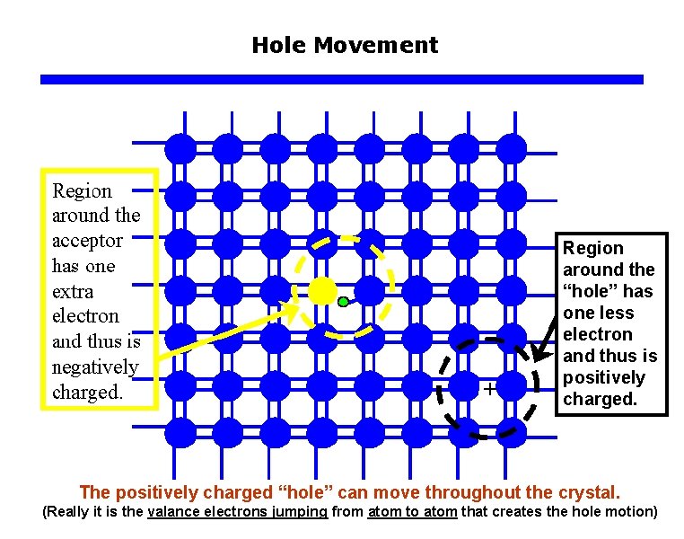
Hole Movement Region around the “hole” has one less electron and thus is positively charged. The positively charged “hole” can move throughout the crystal. (Really it is the valance electrons jumping from atom to atom that creates the hole motion)

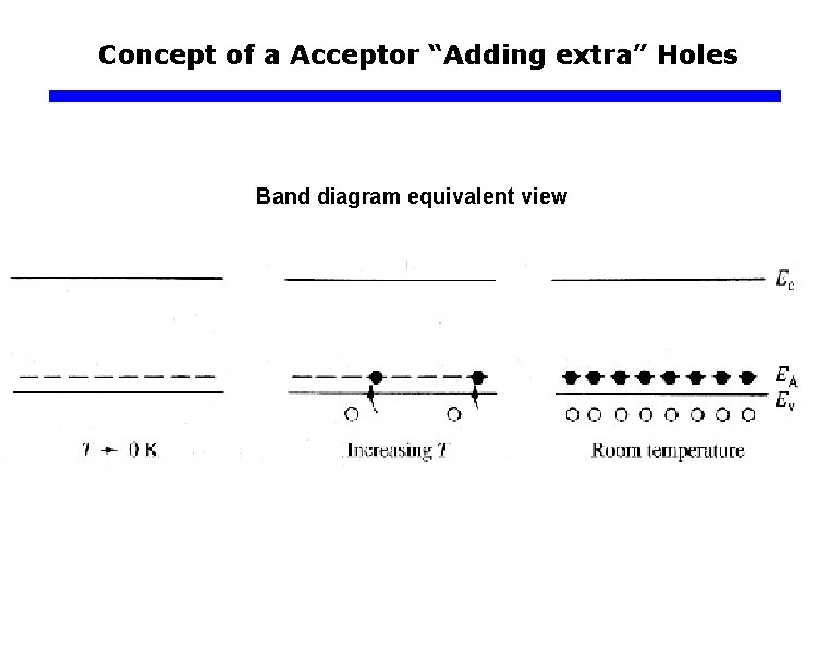
Concept of a Acceptor “Adding extra” Holes Band diagram equivalent view

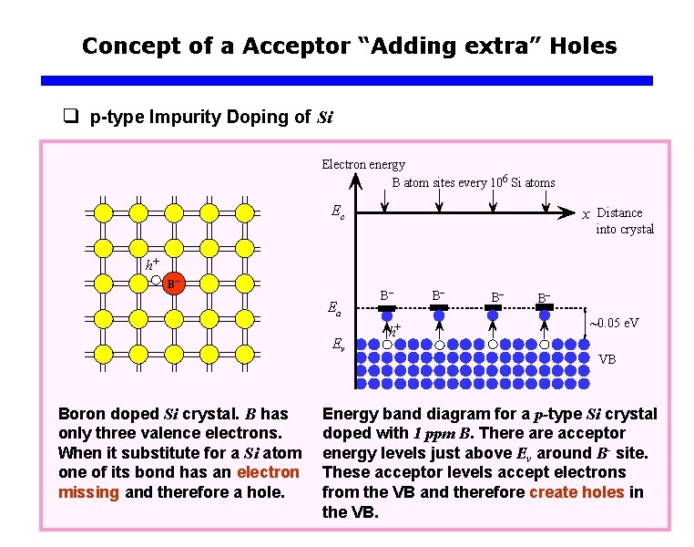
Concept of a Acceptor “Adding extra” Holes q p-type Impurity Doping of Si Electron energy B atom sites every 106 Si atoms Ec x Distance into crystal h+ B– Ea Ev Boron doped Si crystal. B has only three valence electrons. When it substitute for a Si atom one of its bond has an electron missing and therefore a hole. B– h+ B– B– B– ~0. 05 e. V VB Energy band diagram for a p-type Si crystal doped with 1 ppm B. There acceptor energy levels just above Ev around B- site. These acceptor levels accept electrons from the VB and therefore create holes in the VB.

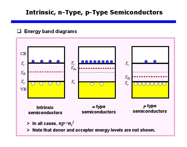
Intrinsic, n-Type, p-Type Semiconductors q Energy band diagrams CB Ec EFi Ev Ec EFn Ec Ev EFp Ev VB Intrinsic semiconductors n-type semiconductors p-type semiconductors Ø In all cases, np=ni 2 Ø Note that donor and acceptor energy levels are not shown.

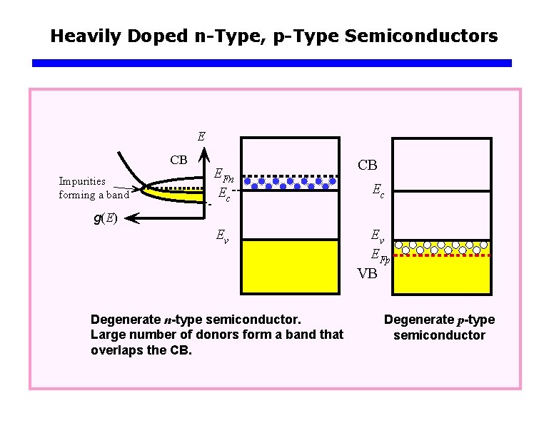
Heavily Doped n-Type, p-Type Semiconductors E CB Impurities forming a band EFn Ec CB Ec g(E) Ev Ev EFp VB Degenerate n-type semiconductor. Large number of donors form a band that overlaps the CB. Degenerate p-type semiconductor

Impurity Doping

Impurity Doping Valence Band

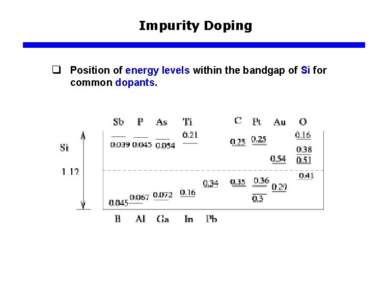
Impurity Doping q Position of energy levels within the bandgap of Si for common dopants.

Summary of Important terms and symbols Bandgap Energy: Energy required to remove a valence electron and allow it to freely conduct. Intrinsic Semiconductor: A “native semiconductor” with no dopants. Electrons in the conduction band equal holes in the valence band. The concentration of electrons (=holes) is the intrinsic concentration, ni. Extrinsic Semiconductor: A doped semiconductor. Many electrical properties controlled by the dopants, not the intrinsic semiconductor. Donor: An impurity added to a semiconductor that adds an additional electron not found in the native semiconductor. Acceptor: An impurity added to a semiconductor that adds an additional hole not found in the native semiconductor. Dopant: Either an acceptor or donor. N-type material: When electron concentrations (n=number of electrons/cm 3) exceed the hole concentration (normally through doping with donors). P-type material: When hole concentrations (p=number of holes/cm 3) exceed the electron concentration (normally through doping with acceptors). Majority carrier: The carrier that exists in higher population (i. e. n if n>p, p if p>n) Minority carrier: The carrier that exists in lower population (i. e. n if n<p, p if p<n) Other important terms: Insulator, semiconductor, metal, amorphous, polycrystalline, crystalline (or single crystal), lattice, unit cell, primitive unit cell, zincblende, lattice constant, elemental semiconductor, compound semiconductor, binary, ternary, quaternary, atomic density, Miller indices