CAPACITANCE AND INDUCTANCE Introduces two passive energy storing


- Slides: 25
CAPACITANCE AND INDUCTANCE Introduces two passive, energy storing devices: Capacitors and Inductors CAPACITORS Store energy in their electric field (electrostatic energy) Model as circuit element INDUCTORS Store energy in their magnetic field Model as circuit element CAPACITOR AND INDUCTOR COMBINATIONS Series/parallel combinations of elements
CAPACITORS First of the energy storage devices to be discussed Typical Capacitors Basic parallel-plates capacitor CIRCUIT REPRESENTATION NOTICE USE OF PASSIVE SIGN CONVENTION
PLATE SIZE FOR EQUIVALENT AIR-GAP CAPACITOR Normal values of capacitance are small. Microfarads is common. For integrated circuits nano or pico farads are not unusual
Basic capacitance law Linear capacitors obey Coulomb’s law C is called the CAPACITANCE of the device and has units of One Farad(F)is the capacitance of a device that can store one Coulomb of charge at one Volt. Linear capacitor circuit representation EXAMPLE Voltage across a capacitor of 2 micro Farads holding 10 m. C of charge V Capacitance in Farads, charge in Coulombs result in voltage in Volts Capacitors can be dangerous!!!
Capacitors only store and release ELECTROSTATIC energy. They do not “create” The capacitor is a passive element and follows the passive sign convention Linear capacitor circuit representation
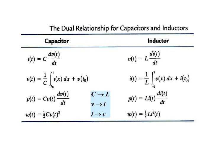
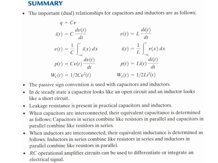
Capacitance Law If the voltage varies the charge varies and there is a displacement current One can also express the voltage across in terms of the current Integral form of Capacitance law The mathematical implication of the integral form is. . . … Or one can express the current through in terms of the voltage across Differential form of Capacitance law Implications of differential form? ? DC or steady state behavior Voltage across a capacitor MUST be continuous A capacitor in steady state acts as an OPEN CIRCUIT
CAPACITOR AS CIRCUIT ELEMENT Ohm’s Law The fact that the voltage is defined through an integral has important implications. . . LEARNING EXAMPLE
CAPACITOR AS ENERGY STORAGE DEVICE Instantaneous power W Energy is the integral of power If t 1 is minus infinity we talk about “energy stored at time t 2. ” If both limits are infinity then we talk about the “total energy stored. ”
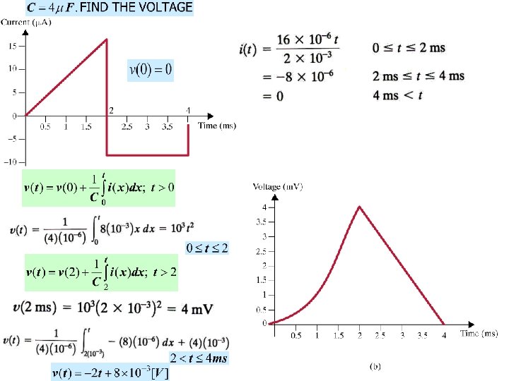
Energy stored in 0 - 6 msec Charge stored at 3 msec EXAMPLE
INDUCTORS Flux lines may extend beyond inductor creating stray inductance effects NOTICE USE OF PASSIVE SIGN CONVENTION Circuit representation for an inductor A TIME VARYING FLUX CREATES A COUNTER EMF AND CAUSES A VOLTAGE TO APPEAR AT THE TERMINALS OF THE DEVICE
A TIME VARYING MAGNETIC FLUX INDUCES A VOLTAGE Induction law FOR A LINEAR INDUCTOR THE FLUX IS PROPORTIONAL TO THE CURRENT DIFFERENTIAL FORM OF INDUCTION LAW THE PROPORTIONALITY CONSTANT, L, IS CALLED THE INDUCTANCE OF THE COMPONENT INDUCTANCE IS MEASURED IN UNITS OF henry (H). DIMENSIONALLY INDUCTORS STORE ELECTROMAGNETIC ENERGY. THEY MAY SUPPLY STORED ENERGY BACK TO THE CIRCUIT BUT THEY CANNOT CREATE ENERGY. THEY MUST ABIDE BY THE PASSIVE SIGN CONVENTION Follow passive sign convention
Differential form of induction law Integral form of induction law A direct consequence of integral form Current MUST be continuous A direct consequence of differential form DC (steady state) behavior Power and Energy stored W J Current in Amps, Inductance in Henrys yield energy in Joules Energy stored on the interval Can be positive or negative
EXAMPLE FIND THE TOTAL ENERGY STORED IN THE CIRCUIT In steady state inductors act as short circuits and capacitors act as open circuits
EXAMPLE L=10 m. H. FIND THE VOLTAGE ENERGY STORED BETWEEN 2 AND 4 ms THE DERIVATIVE OF A STRAIGHT LINE IS ITS SLOPE J THE VALUE IS NEGATIVE BECAUSE THE INDUCTOR IS SUPPLYING ENERGY PREVIOUSLY STORED
CAPACITOR SPECIFICATIONS INDUCTOR SPECIFICATIONS
IDEAL AND PRACTICAL ELEMENTS IDEAL ELEMENTS CAPACITOR/INDUCTOR MODELS INCLUDING LEAKAGE RESISTANCE MODEL FOR “LEAKY” CAPACITOR MODEL FOR “LEAKY” INDUCTORS
SERIES CAPACITORS Series Combination of two capacitors NOTICE SIMILARITY WITH RESITORS IN PARALLEL
PARALLEL CAPACITORS
SERIES INDUCTORS
PARALLEL INDUCTORS COMBINE LIKE RESISTORS CAPACITORS COMBINE LIKE CONDUCTANCES
LEARNING EXAMPLE FLIP CHIP MOUNTING IC WITH WIREBONDS TO THE OUTSIDE GOAL: REDUCE INDUCTANCE IN THE WIRING AND REDUCE THE “GROUND BOUNCE” EFFECT A SIMPLE MODEL CAN BE USED TO DESCRIBE GROUND BOUNCE
MODELING THE GROUND BOUNCE EFFECT IF ALL GATES IN A CHIP ARE CONNECTED TO A SINGLE GROUND THE CURRENT CAN BE QUITE HIGH AND THE BOUNCE MAY BECOME UNACCEPTABLE USE SEVERAL GROUND CONNECTIONS (BALLS) AND ALLOCATE A FRACTION OF THE GATES TO EACH BALL