Calorimeter Algorithm Firmware SLHC Calorimeter Trigger Firmware Studies
![Cluster Weighting Logic Hpos[0] Sign H E 1 |H| Shift <<1 E 2 E Cluster Weighting Logic Hpos[0] Sign H E 1 |H| Shift <<1 E 2 E](https://slidetodoc.com/presentation_image/e4458a94111072d38baf634a5accdb80/image-14.jpg)
- Slides: 32

Calorimeter Algorithm Firmware SLHC Calorimeter Trigger Firmware Studies and Performance T. Gregerson, A. Farmahini-Farahani, J. Liu, B. Buchli, K. Compton, M. Schulte, ECE Department , U. Wisconsin M. Bachtis, S. Dasu, T. Gorski, K. Flood, I. Ross, W. Smith Physics Department , U. Wisconsin W. Plishker, G. Zaki, S. Kedilaya, N. Sane, S. Bhattacharyya ECE Department , U. Maryland October 28, 2009 CMS Upgrade Workshop October 28 2009 Producing FPGA Firmware- 1

Introduction • Design Platform and Methodology • Preliminary Designs and Results • • • Rocket. IO and Buffering Particle Cluster Finder Cluster Weighting and Overlap Filter Cluster Isolation and Jet Reconstruction High-Speed Sorters • DIF Modeling and Unit Testing • Next Steps CMS Upgrade Workshop October 28 2009 Producing FPGA Firmware- 2

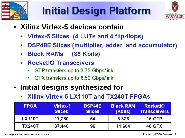
Initial Design Platform • Xilinx Virtex-5 devices contain • • Virtex-5 Slices (4 LUTs and 4 flip-flops) DSP 48 E Slices (multiplier, adder, and accumulator) Block RAMs (36 Kbits) Rocket. IO Transceivers • GTP transfers up to 3. 75 Gbps/link • GTX transfers up to 6. 50 Gbps/link • Initial designs synthesized for • Xilinx Virtex-5 LX 110 T and TX 240 T FPGAs FPGA Virtex-5 Slices DSP 48 E Slices Block RAM (Kbits) Rocket. IO Transceivers LX 110 T 17, 280 64 5, 328 16 GTP TX 240 T 37, 440 96 11, 664 48 GTX CMS Upgrade Workshop October 28 2009 Producing FPGA Firmware- 3

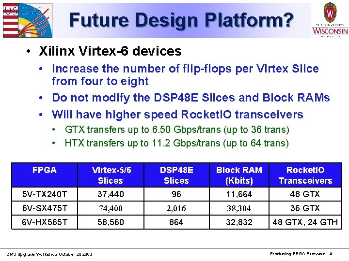
Future Design Platform? • Xilinx Virtex-6 devices • Increase the number of flip-flops per Virtex Slice from four to eight • Do not modify the DSP 48 E Slices and Block RAMs • Will have higher speed Rocket. IO transceivers • GTX transfers up to 6. 50 Gbps/trans (up to 36 trans) • HTX transfers up to 11. 2 Gbps/trans (up to 64 trans) FPGA Virtex-5/6 Slices DSP 48 E Slices Block RAM (Kbits) Rocket. IO Transceivers 5 V-TX 240 T 37, 440 96 11, 664 48 GTX 6 V-SX 475 T 74, 400 2, 016 38, 304 36 GTX 6 V-HX 565 T 58, 560 864 32, 832 48 GTX, 24 GTH CMS Upgrade Workshop October 28 2009 Producing FPGA Firmware- 4

Initial Design Methodology • Designs start with the algorithms • Physicists and engineers collaborate • Evaluate algorithm/implementation tradeoffs • Designs specified using • Verilog and Xilinx Core Generator • Designs implemented and tested using • Xilinx ISE • Model. Sim Xilinx Edition • Initial results obtained for • Rocket. IO, buffering, particle cluster finder, cluster overlap filter, cluster weighting, sorting CMS Upgrade Workshop October 28 2009 Producing FPGA Firmware- 5

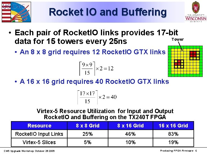
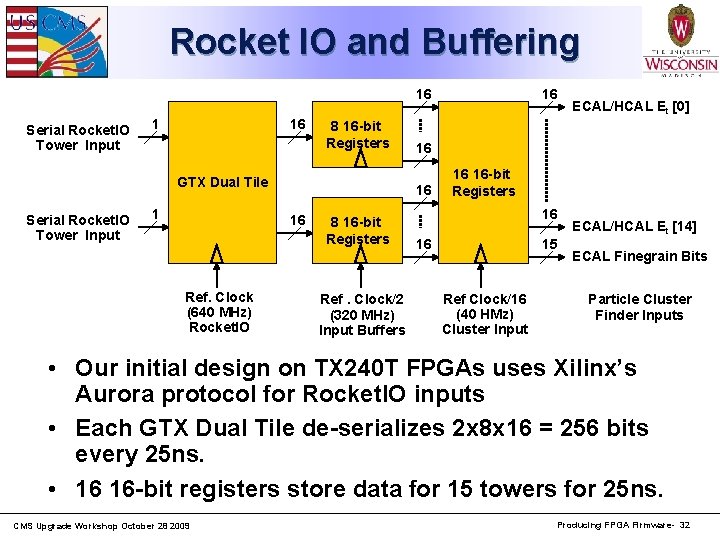
Rocket IO and Buffering • Each pair of Rocket. IO links provides 17 -bit Tower data for 15 towers every 25 ns • An 8 x 8 grid requires 12 Rocket. IO GTX links • A 16 x 16 grid requires 40 Rocket. IO GTX links Virtex-5 Resource Utilization for Input and Output Rocket. IO and Buffering on the TX 240 T FPGA Resource 8 x 8 Grid 8 x 16 Grid 16 x 16 Grid Rocket. IO Input Links 25% 46% 83% Virtex-5 Slices 5% 10% 19% CMS Upgrade Workshop October 28 2009 Producing FPGA Firmware- 6

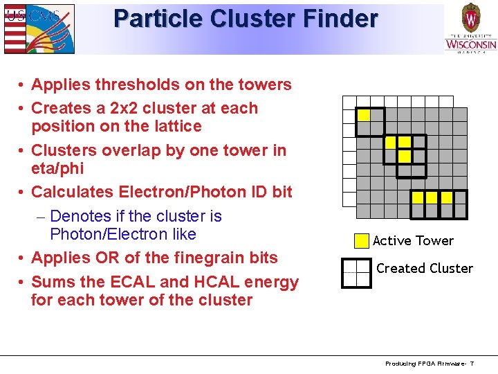
Particle Cluster Finder • Applies thresholds on the towers • Creates a 2 x 2 cluster at each position on the lattice • Clusters overlap by one tower in eta/phi • Calculates Electron/Photon ID bit – Denotes if the cluster is Photon/Electron like • Applies OR of the finegrain bits • Sums the ECAL and HCAL energy for each tower of the cluster Active Tower Created Cluster Producing FPGA Firmware- 7

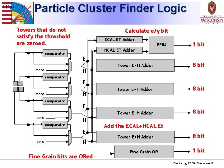
Particle Cluster Finder Logic Towers that do not satisfy the threshold are zeroed. comparator Calculate e/γ bit ECAL ET Adder EPIM HCAL ET Adder E H zero comparator 8 bit Tower E+H Adder 8 bit E H E zero Tower E+H Adder E H zero 1 bit H Fine Grain bits are ORed Add the ECAL+HCAL Et Tower E+H Adder Fine Grain OR 8 bit 1 bit Producing FPGA Firmware- 8

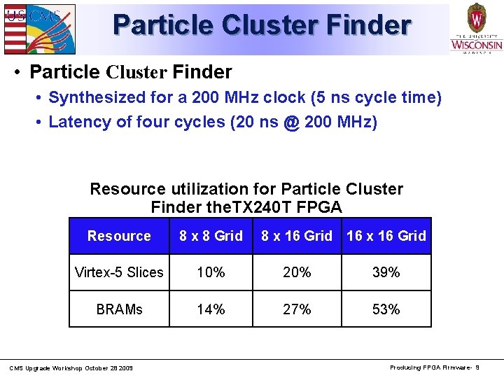
Particle Cluster Finder • Synthesized for a 200 MHz clock (5 ns cycle time) • Latency of four cycles (20 ns @ 200 MHz) Resource utilization for Particle Cluster Finder the. TX 240 T FPGA Resource 8 x 8 Grid Virtex-5 Slices 10% 20% 39% BRAMs 14% 27% 53% CMS Upgrade Workshop October 28 2009 8 x 16 Grid 16 x 16 Grid Producing FPGA Firmware- 9

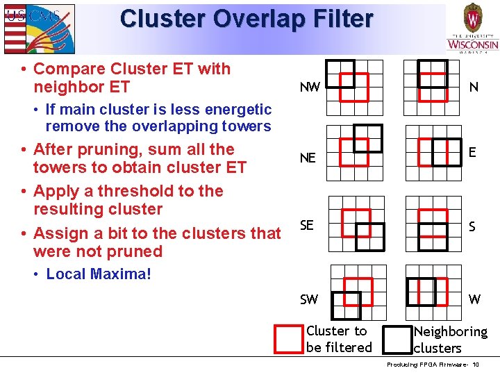
Cluster Overlap Filter • Compare Cluster ET with neighbor ET NW N NE E SE S SW W • If main cluster is less energetic remove the overlapping towers • After pruning, sum all the towers to obtain cluster ET • Apply a threshold to the resulting cluster • Assign a bit to the clusters that were not pruned • Local Maxima! Cluster to be filtered Neighboring clusters Producing FPGA Firmware- 10

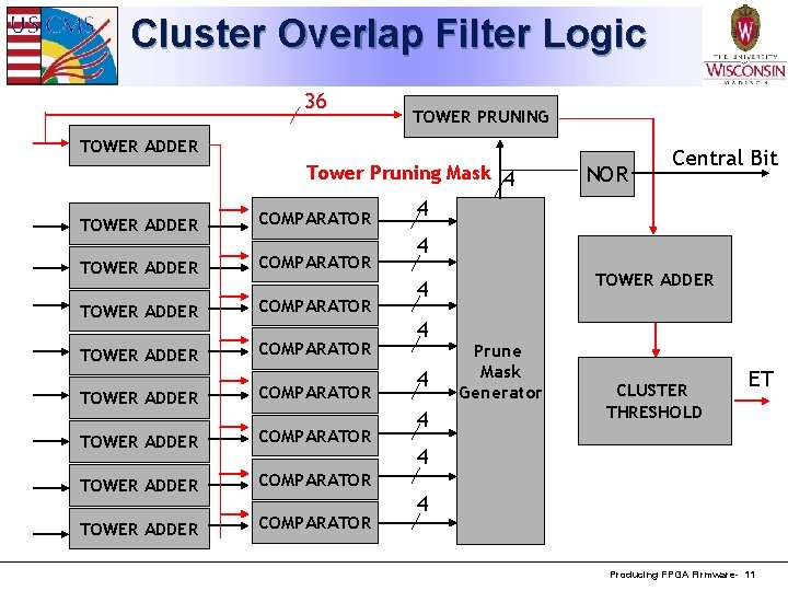
Cluster Overlap Filter Logic 36 TOWER PRUNING TOWER ADDER Tower Pruning Mask 4 TOWER ADDER COMPARATOR TOWER ADDER COMPARATOR NOR Central Bit 4 4 TOWER ADDER 4 4 Prune Mask Generator CLUSTER THRESHOLD ET 4 4 Producing FPGA Firmware- 11

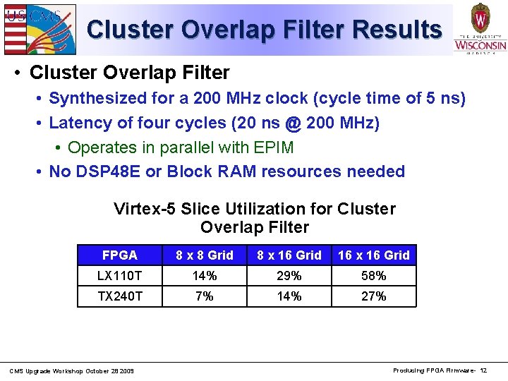
Cluster Overlap Filter Results • Cluster Overlap Filter • Synthesized for a 200 MHz clock (cycle time of 5 ns) • Latency of four cycles (20 ns @ 200 MHz) • Operates in parallel with EPIM • No DSP 48 E or Block RAM resources needed Virtex-5 Slice Utilization for Cluster Overlap Filter FPGA 8 x 8 Grid 8 x 16 Grid 16 x 16 Grid LX 110 T 14% 29% 58% TX 240 T 7% 14% 27% CMS Upgrade Workshop October 28 2009 Producing FPGA Firmware- 12

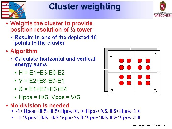
Cluster weighting • Weights the cluster to provide position resolution of ½ tower • Results in one of the depicted 16 points in the cluster • Algorithm • Calculate horizontal and vertical energy sums 0 1 • H = E 1+E 3 -E 0 -E 2 • V = E 2+E 3 -E 0 -E 1 • S = E 1+E 2+E 3+E 4 2 • Hpos = H/S, Vpos = V/S • No division is needed • -1<Hpos<-0. 5, -0. 5<Hpos<0, 0<Hpos<0. 5, 0. 5<Hpos<1. 0 3 • -1<Vpos<-0. 5, -0. 5<Vpos<0, 0<Vpos<0. 5, 0. 5<Vpos<1. 0 Producing FPGA Firmware- 13
![Cluster Weighting Logic Hpos0 Sign H E 1 H Shift 1 E 2 E Cluster Weighting Logic Hpos[0] Sign H E 1 |H| Shift <<1 E 2 E](https://slidetodoc.com/presentation_image/e4458a94111072d38baf634a5accdb80/image-14.jpg)
Cluster Weighting Logic Hpos[0] Sign H E 1 |H| Shift <<1 E 2 E 3 E 4 ADDERS Compare (>) Hpos[1] S |V| Shift <<1 Compare (>) Vpos[1] Sign V Vpos[0] • Signs of H and V plus magnitude comparisons determine Hpos and Vpos (each 2 bits) Producing FPGA Firmware- 14

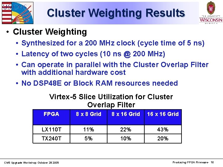
Cluster Weighting Results • Cluster Weighting • Synthesized for a 200 MHz clock (cycle time of 5 ns) • Latency of two cycles (10 ns @ 200 MHz) • Can operate in parallel with the Cluster Overlap Filter with additional hardware cost • No DSP 48 E or Block RAM resources needed Virtex-5 Slice Utilization for Cluster Overlap Filter FPGA 8 x 8 Grid 8 x 16 Grid 16 x 16 Grid LX 110 T 11% 22% 43% TX 240 T 5% 10% 20% CMS Upgrade Workshop October 28 2009 Producing FPGA Firmware- 15

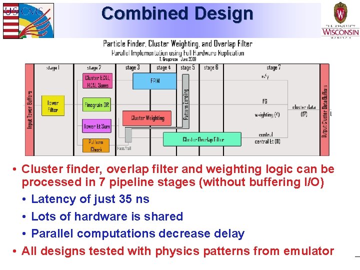
Combined Design • Cluster finder, overlap filter and weighting logic can be processed in 7 pipeline stages (without buffering I/O) • Latency of just 35 ns • Lots of hardware is shared • Parallel computations decrease delay • All designs tested with physics patterns from emulator CMS Upgrade Workshop October 28 2009 Producing FPGA Firmware- 16

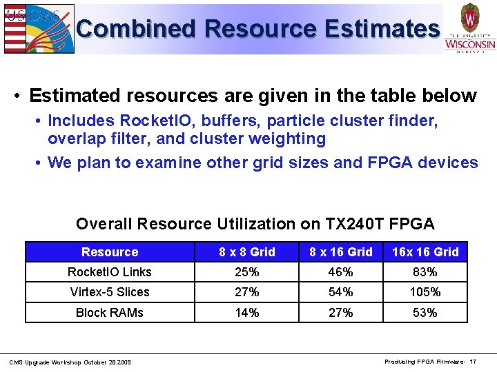
Combined Resource Estimates • Estimated resources are given in the table below • Includes Rocket. IO, buffers, particle cluster finder, overlap filter, and cluster weighting • We plan to examine other grid sizes and FPGA devices Overall Resource Utilization on TX 240 T FPGA Resource 8 x 8 Grid 8 x 16 Grid 16 x 16 Grid Rocket. IO Links 25% 46% 83% Virtex-5 Slices 27% 54% 105% Block RAMs 14% 27% 53% CMS Upgrade Workshop October 28 2009 Producing FPGA Firmware- 17

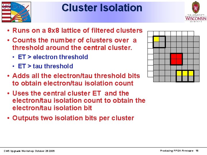
Cluster Isolation • Runs on a 8 x 8 lattice of filtered clusters • Counts the number of clusters over a threshold around the central cluster. • ET > electron threshold • ET > tau threshold • Adds all the electron/tau threshold bits to obtain electron/tau isolation count • Uses the central cluster ET and the electron/tau isolation count to obtain the electron/tau isolation bit • Outputs two isolation bits per cluster CMS Upgrade Workshop October 28 2009 Producing FPGA Firmware- 18

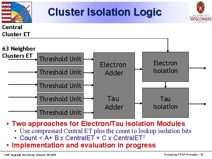
Cluster Isolation Logic Central Cluster ET 63 Neighbor Clusters ET Threshold Unit Electron Adder Electron Isolation Tau Adder Tau Isolation Threshold Unit • Two approaches for Electron/Tau Isolation Modules • Use compressed Central ET plus the count to lookup isolation bits • Count < A+ B x Central. ET + C x Central. ET 2 • Implementation and evaluation in progress CMS Upgrade Workshop October 28 2009 Producing FPGA Firmware- 19

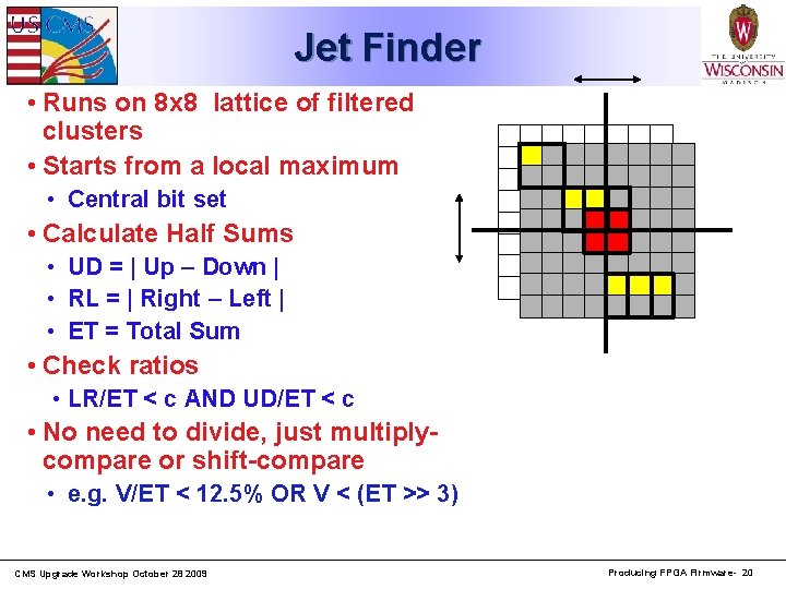
Jet Finder • Runs on 8 x 8 lattice of filtered clusters • Starts from a local maximum • Central bit set • Calculate Half Sums • UD = | Up – Down | • RL = | Right – Left | • ET = Total Sum • Check ratios • LR/ET < c AND UD/ET < c • No need to divide, just multiplycompare or shift-compare • e. g. V/ET < 12. 5% OR V < (ET >> 3) CMS Upgrade Workshop October 28 2009 Producing FPGA Firmware- 20

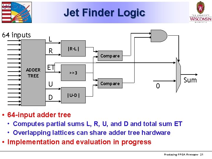
Jet Finder Logic 64 inputs L R ADDER TREE ET |R-L| Compare >>3 U D Compare Sum 0 |U-D| • 64 -input adder tree • Computes partial sums L, R, U, and D and total sum ET • Overlapping lattices can share adder tree hardware • Implementation and evaluation in progress Producing FPGA Firmware- 21

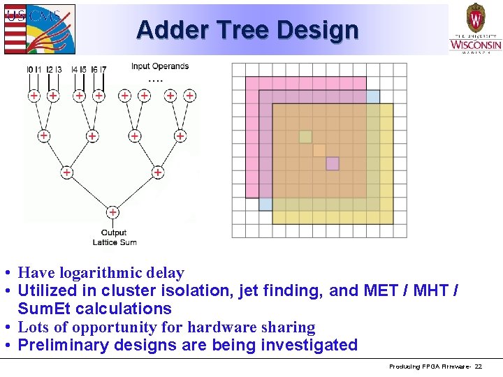
Adder Tree Design • Have logarithmic delay • Utilized in cluster isolation, jet finding, and MET / MHT / Sum. Et calculations • Lots of opportunity for hardware sharing • Preliminary designs are being investigated Producing FPGA Firmware- 22

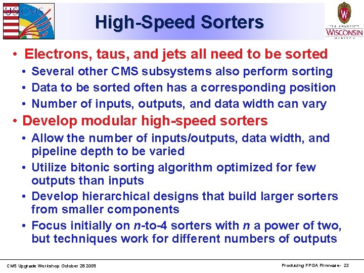
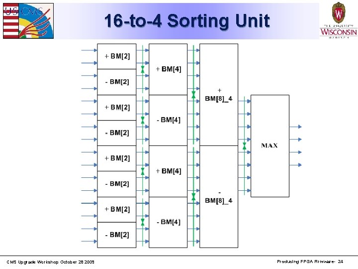
High-Speed Sorters • Electrons, taus, and jets all need to be sorted • Several other CMS subsystems also perform sorting • Data to be sorted often has a corresponding position • Number of inputs, outputs, and data width can vary • Develop modular high-speed sorters • Allow the number of inputs/outputs, data width, and pipeline depth to be varied • Utilize bitonic sorting algorithm optimized for few outputs than inputs • Develop hierarchical designs that build larger sorters from smaller components • Focus initially on n-to-4 sorters with n a power of two, but techniques work for different numbers of outputs CMS Upgrade Workshop October 28 2009 Producing FPGA Firmware- 23

16 -to-4 Sorting Unit CMS Upgrade Workshop October 28 2009 Producing FPGA Firmware- 24

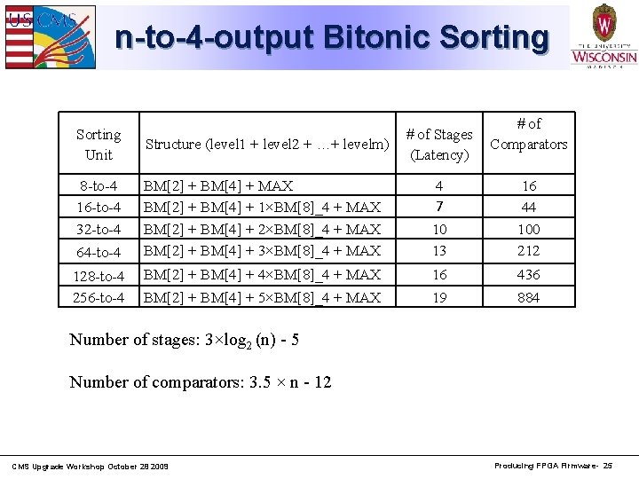
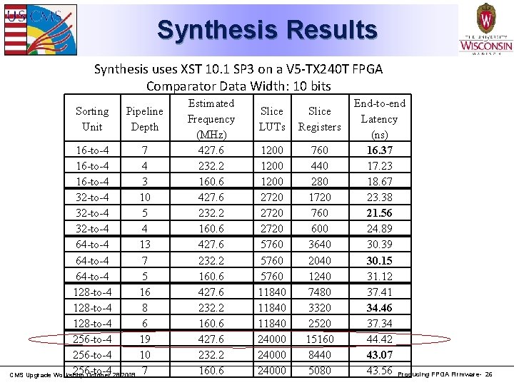
n-to-4 -output Bitonic Sorting Unit 8 -to-4 16 -to-4 32 -to-4 64 -to-4 128 -to-4 256 -to-4 Structure (level 1 + level 2 + …+ levelm) # of Stages (Latency) # of Comparators BM[2] + BM[4] + MAX BM[2] + BM[4] + 1×BM[8]_4 + MAX BM[2] + BM[4] + 2×BM[8]_4 + MAX BM[2] + BM[4] + 3×BM[8]_4 + MAX 4 7 10 13 16 44 100 212 BM[2] + BM[4] + 4×BM[8]_4 + MAX 16 436 BM[2] + BM[4] + 5×BM[8]_4 + MAX 19 884 Number of stages: 3×log 2 (n) - 5 Number of comparators: 3. 5 × n - 12 CMS Upgrade Workshop October 28 2009 Producing FPGA Firmware- 25

Synthesis Results Synthesis uses XST 10. 1 SP 3 on a V 5 -TX 240 T FPGA Comparator Data Width: 10 bits Sorting Unit Pipeline Depth 16 -to-4 7 16 -to-4 4 16 -to-4 3 32 -to-4 10 32 -to-4 5 32 -to-4 4 64 -to-4 13 64 -to-4 7 64 -to-4 5 128 -to-4 16 128 -to-4 8 128 -to-4 6 256 -to-4 19 256 -to-4 10 256 -to-4 CMS Upgrade Workshop October 28 2009 7 Estimated Frequency (MHz) 427. 6 232. 2 160. 6 Slice LUTs Slice Registers 1200 2720 5760 11840 24000 760 440 280 1720 760 600 3640 2040 1240 7480 3320 2520 15160 8440 5080 End-to-end Latency (ns) 16. 37 17. 23 18. 67 23. 38 21. 56 24. 89 30. 39 30. 15 31. 12 37. 41 34. 46 37. 34 44. 42 43. 07 43. 56 Producing FPGA Firmware- 26

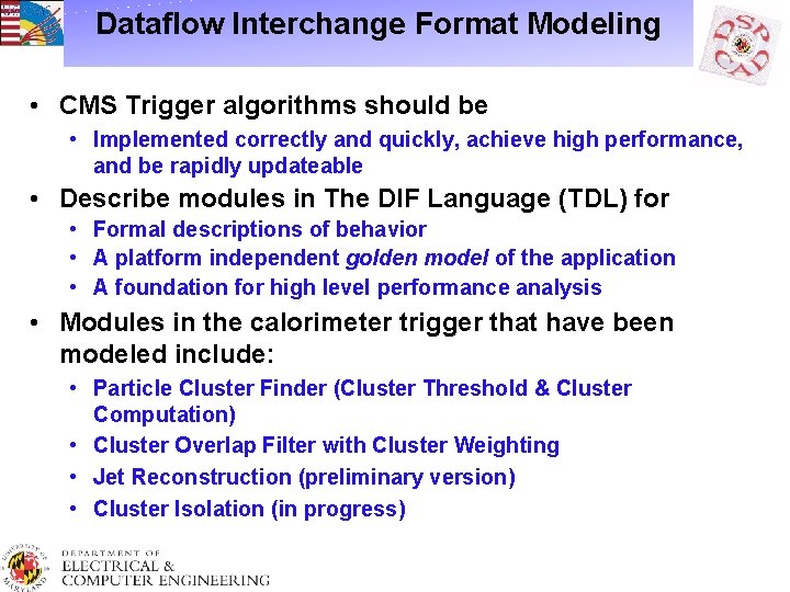
Dataflow Interchange Format Modeling • CMS Trigger algorithms should be • Implemented correctly and quickly, achieve high performance, and be rapidly updateable • Describe modules in The DIF Language (TDL) for • Formal descriptions of behavior • A platform independent golden model of the application • A foundation for high level performance analysis • Modules in the calorimeter trigger that have been modeled include: • Particle Cluster Finder (Cluster Threshold & Cluster Computation) • Cluster Overlap Filter with Cluster Weighting • Jet Reconstruction (preliminary version) • Cluster Isolation (in progress)

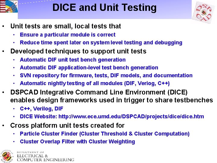
DICE and Unit Testing • Unit tests are small, local tests that • Ensure a particular module is correct • Reduce time spent later on system level testing and debugging • Developed techniques to support unit tests • • Automatic DIF unit test bench generation Automatic DIF application-level test bench generation SVN repository for firmware, tests, DIF models, and documentation Automatic nightly testing of all modules (DIF, Veriog, C++) • DSPCAD Integrative Command Line Environment (DICE) enables design frameworks used in trigger to share testbenches • C++, Verilog, DIF • DICE Website: http: //www. ece. umd. edu/DSPCAD/projects/dice. htm • Cross platform unit tests created for • Particle Cluster Finder (Cluster Threshold & Cluster Computation) • Cluster Overlap Filter with Cluster Weighting

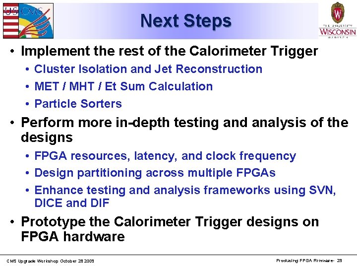
Next Steps • Implement the rest of the Calorimeter Trigger • Cluster Isolation and Jet Reconstruction • MET / MHT / Et Sum Calculation • Particle Sorters • Perform more in-depth testing and analysis of the designs • FPGA resources, latency, and clock frequency • Design partitioning across multiple FPGAs • Enhance testing and analysis frameworks using SVN, DICE and DIF • Prototype the Calorimeter Trigger designs on FPGA hardware CMS Upgrade Workshop October 28 2009 Producing FPGA Firmware- 29

Questions? CMS Upgrade Workshop October 28 2009 Producing FPGA Firmware- 30

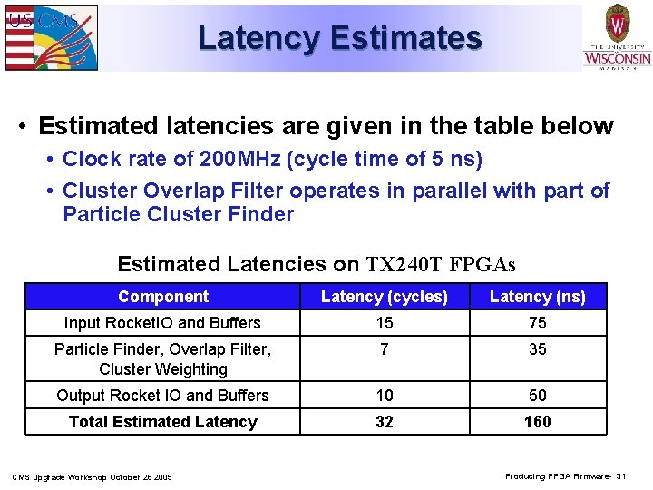
Latency Estimates • Estimated latencies are given in the table below • Clock rate of 200 MHz (cycle time of 5 ns) • Cluster Overlap Filter operates in parallel with part of Particle Cluster Finder Estimated Latencies on TX 240 T FPGAs Component Latency (cycles) Latency (ns) Input Rocket. IO and Buffers 15 75 Particle Finder, Overlap Filter, Cluster Weighting 7 35 Output Rocket IO and Buffers 10 50 Total Estimated Latency 32 160 CMS Upgrade Workshop October 28 2009 Producing FPGA Firmware- 31

Rocket IO and Buffering 16 Serial Rocket. IO Tower Input 1 16 8 16 -bit Registers GTX Dual Tile Serial Rocket. IO Tower Input 1 Ref. Clock (640 MHz) Rocket. IO 8 16 -bit Registers Ref. Clock/2 (320 MHz) Input Buffers ECAL/HCAL Et [0] 16 16 16 -bit Registers 16 16 15 Ref Clock/16 (40 HMz) Cluster Input ECAL/HCAL Et [14] ECAL Finegrain Bits Particle Cluster Finder Inputs • Our initial design on TX 240 T FPGAs uses Xilinx’s Aurora protocol for Rocket. IO inputs • Each GTX Dual Tile de-serializes 2 x 8 x 16 = 256 bits every 25 ns. • 16 16 -bit registers store data for 15 towers for 25 ns. CMS Upgrade Workshop October 28 2009 Producing FPGA Firmware- 32