Cache Memory Chapter 4 Characteristics Location Capacity Unit


 • Sequential • Start at the beginning and read through in")
 • Random • In this method, any location of the memory")
 • Time between presenting the address and getting the valid")


 bits • Number of")


 bits • Number of")


 bits • Number")


 Direct mapping • No choice • Each block only maps to")
 Associative & Set Associative • Hardware implemented algorithm (speed) • Least")


 and the external cache designated as level 2 (L 2).")
 For 8 kbytes and 16 kbyte L")


 Cache Line Size (words)")


- Slides: 79
Cache Memory Chapter 4
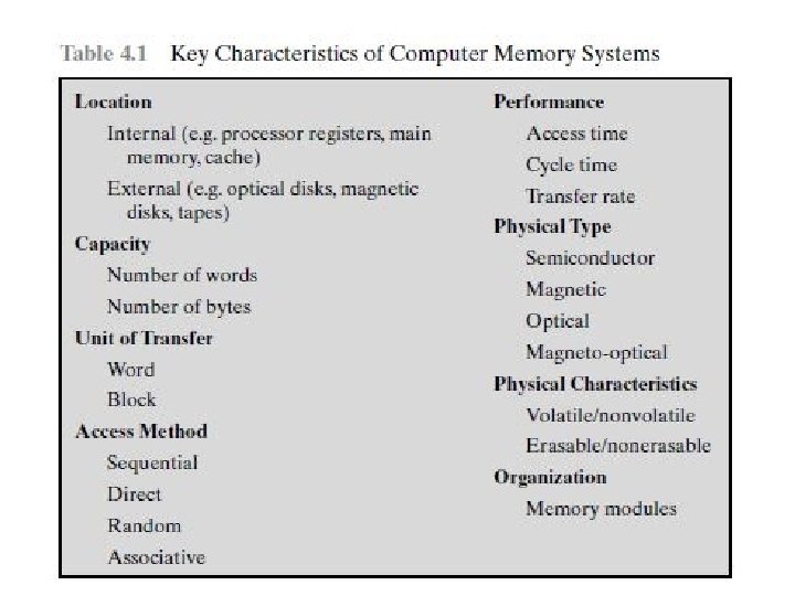
Characteristics • Location • Capacity • Unit of transfer • Access method • Performance • Physical type • Physical characteristics • Organisation
Location • CPU • Internal memory is often equated with main memory. But there are other forms of internal memory. The processor requires its own local memory the form of registers. • Cache is another form of internal memory. • External memory consists of peripheral storage devices, such as disk and tape, that are accessible to the processor via I/O controllers
Capacity • Word size • For internal memory, this is typically expressed in terms of bytes (1 byte 8 bits) or words • The natural unit of organisation is word • Number of words • or Bytes • External memory capacity is typically expressed in terms of bytes. • Common word lengths are 8, 16, and 32 bits
Unit of Transfer • Internal • For internal memory, the unit of transfer is equal to the number of electrical lines into and out of the memory module. • Usually governed by data bus width • External • Usually a block which is much larger than a word • Word: The “natural” unit of organization of memory. The size of the word is typically equal to the number of bits used to represent an integer and to the instruction length. • Addressable unit • Smallest location which can be uniquely addressed • Word internally • Cluster on M$ disks
Access Methods (1) • Sequential • Start at the beginning and read through in order • Access time depends on location of data and previous location • e. g. tape • Direct • In this method, the particular location of the memory can be accessed directly like accessing in Array. This method is a combination of two access methods(random and seqential). The access time depends on both the memory organization and characteristics of storage technology. The access is semi-random or direct. or • Individual blocks have unique address • Access is by jumping to vicinity plus sequential search counting, or waiting to reach the final location • access time is variable • e. g. disk
Access Methods (2) • Random • In this method, any location of the memory can be accessed randomly like accessing in Array. Physical locations are independent in this access method • Individual addresses identify locations exactly • Access time is independent of location or previous access • e. g. RAM • Associative • In this memory, a word is accessed rather than its address. This access method is a special type of random access method. Application of thus direct memory access is Cache memory. • Data is located by a comparison with contents of a portion of the store • Access time is independent of location or previous access • e. g. cache
Performance • Access time(latency) • Time between presenting the address and getting the valid data • Memory Cycle time • consists of the access time plus any additional time required before a second access can commence • Cycle time is access + recovery • Transfer Rate • Rate at which data can be moved • This is the rate at which data can be transferred into or out of a memory unit. For randomaccess memory, it is equal to 1/(cycle time).
Memory Hierarchy • Registers • In CPU • Internal or Main memory • May include one or more levels of cache • “RAM” • External memory • Backing store
Memory Hierarchy - Diagram
• • • As one goes down the hierarchy, the following occur: a. Decreasing cost per bit b. Increasing capacity c. Increasing access time d. Decreasing frequency of access of the memory by the processor
Physical Types • Semiconductor • RAM • Magnetic • Disk & Tape • Optical • CD & DVD • Others • Bubble memory is a type of non-volatile computer memory that uses a thin film of a magnetic material to hold small magnetized areas, known as bubbles or domains, each storing one bit of data • Hologram Holographic memory is a three-dimensional data storage system that can store information at high density inside the crystal or photopolymer. It is a memory that can store information in the form of holographic image (hologram) Like other media, holographic media is divided into write once (where the storage medium undergoes some irreversible change), and rewritable media (where the change is reversible).
Physical Characteristics • Decay • Volatility • Erasable • Power consumption
Organisation • Physical arrangement of bits into words • Not always obvious • e. g. interleaved
The Bottom Line • design constraints on a computer’s memory can be summed up by three questions • How much? • Capacity • How fast? • Time is money • How expensive?
Hierarchy List • Registers • L 1 Cache • L 2 Cache • Main memory • Disk cache • Disk • Optical • Tape
So you want fast? • It is possible to build a computer which uses only static RAM (see later) • This would be very fast • This would need no cache • How can you cache? • This would cost a very large amount
Locality of Reference • locality of reference, also known as the principle of locality, is the tendency of a processor to access the same set of memory locations repetitively over a short period of time. • During the course of the execution of a program, memory references tend to cluster • e. g. loops • Programs typically contain a number of iterative loops and subroutines. Once a loop or subroutine is entered, there are repeated references to a small set of instructions. • Similarly, operations on tables and arrays involve access to a clustered set of data words. Over a long period of time, the clusters in use change, but over a short period of time, the processor is primarily working with fixed clusters of memory references.
Cache • Small amount of fast memory • Sits between normal main memory and CPU • May be located on CPU chip or module
Cache operation – overview • CPU requests contents of memory location • Check cache for this data • If present, get from cache (fast) • If not present, read required block from main memory to cache • Then deliver from cache to CPU • Cache includes tags to identify which block of main memory is in each cache slot
Cache and Main Memory
• Figure 4. 3 b depicts the use of multiple levels of cache. The L 2 cache is slower • and typically larger than the L 1 cache, and the L 3 cache is slower and typically • larger than the L 2 cache
Cache/Main Memory Structure
• Figure 4. 4 depicts the structure of a cache/main-memory system. • Main memory consists of up to 2^n addressable words, with each word having a unique n-bit address. • For mapping purposes, this memory is considered to consist of a number of fixed length blocks of K words each. • That is, there are M= 2 n/K blocks in main memory. • The cache consists of m blocks, called lines. Each line contains K words, plus a tag of • a few bits. Each line also includes control bits (not shown), such as a bit to indicate whether the line has been modified since being loaded into the cache. • The length of a line, not including tag and control bits, is the line size. • The line size may be as small as 32 bits, with each “word” being a single byte; in this case the line size is 4 bytes. • The number of lines is considerably less than the number of main memory blocks • (m<< M)
Cache Read Operation - Flowchart
• Figure 4. 5 illustrates the read operation. The processor generates the read address (RA) of a word to be read. • If the word is contained in the cache, it is delivered to the processor. Otherwise, the block containing that word is loaded into the cache, and the word is delivered to the processor
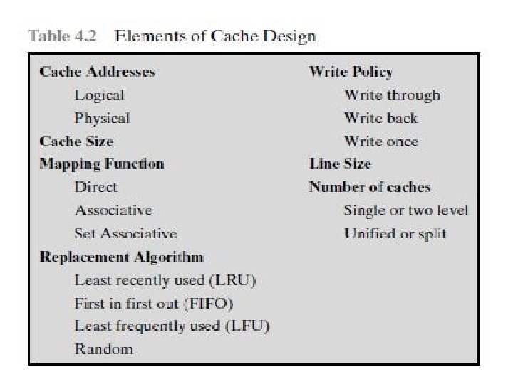
Cache Design • Addressing • Size • Mapping Function • Replacement Algorithm • Write Policy • Block Size • Number of Caches
Cache Addressing • Where does cache sit? • Between processor and virtual memory management unit • Between MMU and main memory • Logical cache (virtual cache) stores data using virtual addresses • Processor accesses cache directly, without going through the MMU, not thorough physical cache • Cache access faster, before MMU address translation • Virtual addresses use same address space for different applications • Must flush cache on each context switch • Physical cache stores data using main memory physical addresses
Size does matter • Cost • More cache is expensive • Speed • More cache is faster (up to a point) • Checking cache for data takes time
Typical Cache Organization
Comparison of Cache Sizes L 1 cache L 2 cache L 3 cache Mainframe Year of Introduction 1968 16 to 32 KB — — PDP-11/70 Minicomputer 1975 1 KB — — VAX 11/780 Minicomputer 1978 16 KB — — IBM 3033 Mainframe 1978 64 KB — — IBM 3090 Mainframe 1985 128 to 256 KB — — Intel 80486 PC 1989 8 KB — — Pentium PC 1993 8 KB/8 KB 256 to 512 KB — Power. PC 601 PC 1993 32 KB — — Power. PC 620 PC 1996 32 KB/32 KB — — Power. PC G 4 PC/server 1999 32 KB/32 KB 256 KB to 1 MB 2 MB IBM S/390 G 4 Mainframe 1997 32 KB 256 KB 2 MB IBM S/390 G 6 Mainframe 1999 256 KB 8 MB — Pentium 4 2000 8 KB/8 KB 256 KB — 2000 64 KB/32 KB 8 MB — CRAY MTAb PC/server High-end server/ supercomputer Supercomputer 2000 8 KB 2 MB — Itanium PC/server 2001 16 KB/16 KB 96 KB 4 MB SGI Origin 2001 High-end server 2001 32 KB/32 KB 4 MB — Itanium 2 PC/server 2002 32 KB 256 KB 6 MB IBM POWER 5 High-end server 2003 64 KB 1. 9 MB 36 MB CRAY XD-1 Supercomputer 2004 64 KB/64 KB 1 MB — Processor Type IBM 360/85 IBM SP
Mapping Function • The choice of the mapping function dictates how the cache is organized. Three techniques can be used: direct, associative, and set associative. • Because there are fewer cache lines than main memory blocks, an algorithm is needed for mapping main memory blocks into cache lines. • Cache of 64 k. Byte • Cache block of 4 bytes • i. e. cache is 16 k (214) lines of 4 bytes • 16 MBytes main memory • 24 bit address • (224=16 M)
Direct Mapping • Each block of main memory maps to only one cache line • i. e. if a block is in cache, it must be in one specific place • Address is in two parts • Least Significant w bits identify unique word within a block of main memory • Most Significant s bits specify one memory block • The MSBs are split into a cache line field r and a tag of s-r (most significant) • The cache logic interprets these s bits as a tag of s - r bits (most significant portion)
Direct Mapping Address Structure Tag s-r 8 Line or Slot r 14 • 24 bit address • 2 bit word identifier (4 byte block) • 22 bit block identifier • 8 bit tag (=22 -14) • 14 bit slot or line • No two blocks in the same line have the same Tag field • Check contents of cache by finding line and checking Tag Word w 2
Direct Mapping from Cache to Main Memory
Direct Mapping Cache Line Table The effect of this mapping is that blocks of main memory are assigned to lines of the cache as follows Cache line Main Memory blocks held 0 0, m, 2 m, 3 m… 2 s-m 1 1, m+1, 2 m+1… 2 s-m+1 … m-1, 2 m-1, 3 m-1… 2 s-1 Thus, the use of a portion of the address as a line number provides a unique mapping of each block of main memory into the cache.
Direct Mapping Cache Organization
Direc t Map ping Exa mple
Direct Mapping Summary • Address length = (s + w) bits • Number of addressable units = 2 s+w words or bytes • Block size = line size = 2 w words or bytes • Number of blocks in main memory = 2 s+ w/2 w = 2 s • Number of lines in cache = m = 2 r • Size of tag = (s – r) bits
Direct Mapping pros & cons • Simple • Inexpensive • Fixed location for given block • If a program accesses 2 blocks that map to the same line repeatedly, cache misses are very high • The direct mapping technique is simple and inexpensive to implement. Its main disadvantage is that there is a fixed cache location for any given block. Thus, if a program happens to reference words repeatedly from two different blocks that • map into the same line, then the blocks will be continually swapped in the cache, and the hit ratio will be low (a phenomenon known as thrashing).
Victim Cache • Lower miss penalty • Remember what was discarded • Already fetched • Use again with little penalty • Fully associative • 4 to 16 cache lines • Between direct mapped L 1 cache and next memory level • One approach to lower the miss penalty is to remember what was discarded in case it is needed again. Since the discarded data has already been fetched, it can be used again at a small cost. Such recycling is possible using a victim cache. • Victim cache was originally proposed as an approach to reduce the conflict misses of direct mapped caches without affecting its fast access time. • Victim cache is a fully associative cache, whose size is typically 4 to 16 cache lines, residing between a direct mapped L 1 cache and the next level of memory.
Associative Mapping • A main memory block can load into any line of cache • Memory address is interpreted as tag and word • Tag uniquely identifies block of memory • Every line’s tag is examined for a match , To determine whether a block is in the cache, • Cache searching gets expensive
Associative Mapping from Cache to Main Memory
Fully Associative Cache Organization
Associative Mapping Example
Associative Mapping Address Structure Word 2 bit Tag 22 bit • 22 bit tag stored with each 32 bit block of data • Compare tag field with tag entry in cache to check for hit • Least significant 2 bits of address identify which 16 bit word is required from 32 bit data block • e. g. • Address • FFFFFC Tag FFFFFC Data 2468 Cache line 3 FFF
Associative Mapping Summary • Address length = (s + w) bits • Number of addressable units = 2 s+w words or bytes • Block size = line size = 2 w words or bytes • Number of blocks in main memory = 2 s+ w/2 w = 2 s • Number of lines in cache = undetermined • Size of tag = s bits
Set Associative Mapping • Cache is divided into a number of sets • Each set contains a number of lines • As with associative mapping, each word maps into multiple cache lines. For set-associative mapping, each word maps into all the cache lines in a specific set, so that main memory block B 0 smaps into set 0, and so on • A given block maps to any line in a given set • e. g. Block B can be in any line of set i • e. g. 2 lines per set • 2 way associative mapping • A given block can be in one of 2 lines in only one set
Set Associative Mapping Example • 13 bit set number • Block number in main memory is modulo 213 • 000000, 00 A 000, 00 B 000, 00 C 000 … map to same set
Mapping From Main Memory to Cache: v Associative
Mapping From Main Memory to Cache: k-way Associative
K-Way Set Associative Cache Organization
Set Associative Mapping Address Structure Tag 9 bit Set 13 bit • Use set field to determine cache set to look in • Compare tag field to see if we have a hit • e. g • Address • 1 FF 7 FFC 1 FF • 001 7 FFC 001 Tag Data 12345678 11223344 Set number 1 FFF Word 2 bit
Two Way Set Associative Mapping Example
Set Associative Mapping Summary • Address length = (s + w) bits • Number of addressable units = 2 s+w words or bytes • Block size = line size = 2 w words or bytes • Number of blocks in main memory = 2 d • Number of lines in set = k • Number of sets = v = 2 d • Number of lines in cache = kv = k * 2 d • Size of tag = (s – d) bits
Direct and Set Associative Cache Performance Differences • Significant up to at least 64 k. B for 2 -way • Difference between 2 -way and 4 -way at 4 k. B much less than 4 k. B to 8 k. B • Cache complexity increases with associativity • Not justified against increasing cache to 8 k. B or 16 k. B • Above 32 k. B gives no improvement • (simulation results)
Figure 4. 16 Varying Associativity over Cache Size
Replacement Algorithms (1) Direct mapping • No choice • Each block only maps to one line • Replace that line • Once the cache has been filled, when a new block is brought into the cache, one of the existing blocks must be replaced. • For direct mapping, there is only one possible line for any particular block, and no choice is possible. For the associative and set associative techniques, a replacement algorithm is needed
Replacement Algorithms (2) Associative & Set Associative • Hardware implemented algorithm (speed) • Least Recently used (LRU) • e. g. in 2 way set associative • Which of the 2 block is lru? • First in first out (FIFO) • replace block that has been in cache longest • Least frequently used • replace block which has had fewest hits • Random
Write Policy • Must not overwrite a cache block unless main memory is up to date • Multiple CPUs may have individual caches • I/O may address main memory directly • When a block that is resident in the cache is to be replaced, there are two cases to consider. • If the old block in the cache has not been altered, then it may be overwritten with a new block without first writing out the old block. • If at least one write operation has been performed on a word in that line of the cache, then main memory must be updated by writing the line of cache out to the block of memory before bringing in the new block. • There are two problems to contend with. First, more than one device may have access to main memory. For example, an I/O module may be able to read-write directly to memory. • If a word has been altered only in the cache, then the corresponding memory word is invalid. • Further, if the I/O device has altered main memory, then the cache word is invalid. • A more complex problem occurs when multiple processors are attached to the same bus and each processor has its own local cache.
Write through • All writes go to main memory as well as cache ensuring that main memory is always valid • Multiple CPUs can monitor main memory traffic to keep local (to CPU) cache(own) up to date • Lots of traffic Disadvantage • Slows down writes • Remember bogus write through caches!
Write back • Updates initially made in cache only • Update bit for cache slot is set when update occurs • When an update occurs, a dirty bit, or use bit, associated with the line is set • If block is to be replaced, write to main memory only if update bit(dirty bit)is set. • The problem with write back is that portions of main memory are invalid, and hence accesses by I/O modules can be allowed only through the cache • Other caches get out of sync • I/O must access main memory through cache • Experience shown 15% of memory references are writes
Line Size • When a block of data is retrieved and placed in the cache Retrieve desired word but a number of adjacent words as well • Increased block size will increase hit ratio at first not only • the principle of locality • Hit ratio will decreases as block becomes even bigger • Probability of using newly fetched information becomes less than probability of reusing replaced • Larger blocks • Reduce number of blocks that fit in cache • Data overwritten shortly after being fetched • Each additional word is less local so less likely to be needed • No definitive optimum value has been found • 8 to 64 bytes seems reasonable • For HPC systems, 64 - and 128 -byte Cache lines are most common
No of Cache Multilevel Caches • High logic density enables caches on chip • • • Faster than bus access • Frees bus for other transfers Compared with a cache reachable via an external bus, the on-chip cache reduces the processor’s external bus activity and therefore speeds up execution times and increases overall system performance. When the requested instruction or data is found in the on-chip cache, the bus access is eliminated. Because of the short data paths internal to the processor, compared with bus lengths, on-chip cache accesses will complete appreciably faster than would even zero-wait state bus cycles. Furthermore, during this period the bus is free to support other transfers • Common to use both on and off chip cache • The inclusion of an on-chip cache leaves open the question of whether an offchip, or external, cache is still desirable. • Typically, the answer is yes, and most contemporary designs include both on-chip and external caches. • The simplest such organization is known as a two-level cache, with the internal cache designated as level
• The reason for including an L 2 cache is the following: If there is no L 2 cache and the processor makes an access request for a memory location not in the L 1 cache, then the processor must access DRAM or ROM memory across the bus. Due to the typically slow bus speed and slow memory access time, this results in poor performance. • On the other hand, if an L 2 SRAM (static RAM) cache is used, then frequently the missing information can be quickly retrieved. • If the SRAM is fast enough to match the bus speed, then the data can be accessed using a zero-wait state transaction, the fastest type of bus transfer
• (L 1) and the external cache designated as level 2 (L 2). • L 1 on chip, L 2 off chip in static RAM • L 2 access much faster than DRAM or ROM • L 2 often uses separate data path • L 2 may now be on chip • Resulting in L 3 cache • Bus access or now on chip…
Hit Ratio (L 1 & L 2) For 8 kbytes and 16 kbyte L 1
Unified v Split Caches • One cache for data and instructions or two, one for data and one for instructions • Advantages of unified cache • Higher hit rate • Balances load of instruction and data fetch • Only one cache to design & implement • Advantages of split cache • Eliminates cache contention between instruction fetch/decode unit and execution unit • Important in pipelining
Pentium 4 Cache • 80386 – no on chip cache • 80486 – 8 k using 16 byte lines and four way set associative organization • Pentium (all versions) – two on chip L 1 caches • Data & instructions • Pentium III – L 3 cache added off chip • Pentium 4 • L 1 caches • 8 k bytes • 64 byte lines • four way set associative • L 2 cache • • Feeding both L 1 caches 256 k 128 byte lines 8 way set associative • L 3 cache on chip
Intel Cache Evolution Problem Solution Processor on which feature first appears Add external cache using faster memory technology. 386 External memory slower than the system bus. Increased processor speed results in external bus becoming a bottleneck for cache access. Move external cache on-chip, operating at the same speed as the processor. 486 Internal cache is rather small, due to limited space on chip Add external L 2 cache using faster technology than main memory Create separate data and instruction caches. Pentium Create separate back-side bus that runs at higher speed than the main (front-side) external bus. The BSB is dedicated to the L 2 cache. Pentium Pro Contention occurs when both the Instruction Prefetcher and the Execution Unit simultaneously require access to the cache. In that case, the Prefetcher is stalled while the Execution Unit’s data access takes place. Increased processor speed results in external bus becoming a bottleneck for L 2 cache access. Some applications deal with massive databases and must have rapid access to large amounts of data. The on-chip caches are too small. Move L 2 cache on to the processor chip. Pentium II Add external L 3 cache. Pentium III Move L 3 cache on-chip. Pentium 4
Pentium 4 Block Diagram
Pentium 4 Core Processor • Fetch/Decode Unit • Fetches instructions from L 2 cache • Decode into micro-ops • Store micro-ops in L 1 cache • Out of order execution logic • Schedules micro-ops • Based on data dependence and resources • May speculatively execute • Execution units • Execute micro-ops • Data from L 1 cache • Results in registers • Memory subsystem • L 2 cache and systems bus
Pentium 4 Design Reasoning • Decodes instructions into RISC like micro-ops before L 1 cache • Micro-ops fixed length • Superscalar pipelining and scheduling • Pentium instructions long & complex • Performance improved by separating decoding from scheduling & pipelining • (More later – ch 14) • Data cache is write back • Can be configured to write through • L 1 cache controlled by 2 bits in register • CD = cache disable • NW = not write through • 2 instructions to invalidate (flush) cache and write back then invalidate • L 2 and L 3 8 -way set-associative • Line size 128 bytes
ARM Cache Features Core Cache Type Cache Size (k. B) Cache Line Size (words) Associativity Location Write Buffer Size (words) ARM 720 T Unified 8 4 4 -way Logical 8 ARM 920 T Split 16/16 D/I 8 64 -way Logical 16 ARM 926 EJ-S Split 4 -128/4 -128 D/I 8 4 -way Logical 16 ARM 1022 E Split 16/16 D/I 8 64 -way Logical 16 ARM 1026 EJ-S Split 4 -128/4 -128 D/I 8 4 -way Logical 8 Intel Strong. ARM Split 16/16 D/I 4 32 -way Logical 32 Intel Xscale Split 32/32 D/I 8 32 -way Logical 32 ARM 1136 -JF-S Split 4 -64/4 -64 D/I 8 4 -way Physical 32
ARM Cache Organization • Small FIFO write buffer • • Enhances memory write performance Between cache and main memory Small c. f. cache Data put in write buffer at processor clock speed Processor continues execution External write in parallel until empty If buffer full, processor stalls Data in write buffer not available until written • So keep buffer small
ARM Cache and Write Buffer Organization
Internet Sources • Manufacturer sites • Intel • ARM • Search on cache