Bulk crystal growth melting points silicon 1420 C
Bulk crystal growth • melting points – silicon: 1420˚ C – Ga. As: 1238˚ C – quartz: 1732˚ C • starting material: metallurgical-grade silicon – by mixing with carbon, Si. O 2 reduced in arc furnace • T > 1780˚C: Si. C + Si. O 2 ® Si + Si. O + CO – common impurities • • Al: 1600 ppm (1 ppm = 5 x 1016 cm-3) B: 40 ppm Fe: 2000 ppm P: 30 ppm – used mostly as an additive in steel Dean P. Neikirk © 1999, last update 30 October 2020 1 Dept. of ECE, Univ. of Texas at Austin
Preparation of electronic-grade silicon • gas phase purification used to produce high purity silicon – ~ 600˚C – crud + Si + HCl ® • • Si. Cl 4 (silicon tetrachloride) Si. Cl 3 H (trichlorosilane) Si. Cl 2 H 2 (dichlorosilane) chlorides of impurities – trichlorosilane (liquid at rm temp), further purification via fractional distillation • now reverse reaction – 2 Si. HCl 3 + 2 H 2 (heat) ® 2 Si + 6 HCl – after purification get • • • Al: below detection B: < 1 ppb (1 ppb = 5 x 1013 cm-3) Fe: 4 ppm P: < 2 ppb Sb: 1 ppb Au: 0. 1 ppb Dean P. Neikirk © 1999, last update 30 October 2020 2 Dept. of ECE, Univ. of Texas at Austin
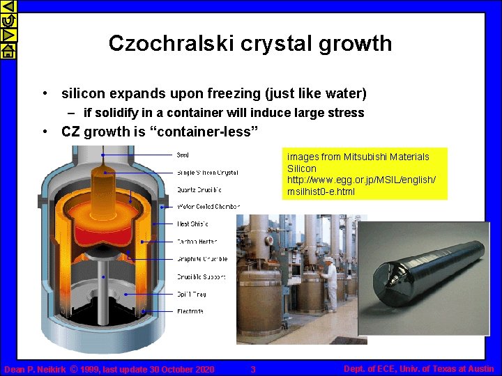
Czochralski crystal growth • silicon expands upon freezing (just like water) – if solidify in a container will induce large stress • CZ growth is “container-less” images from Mitsubishi Materials Silicon http: //www. egg. or. jp/MSIL/english/ msilhist 0 -e. html Dean P. Neikirk © 1999, last update 30 October 2020 3 Dept. of ECE, Univ. of Texas at Austin
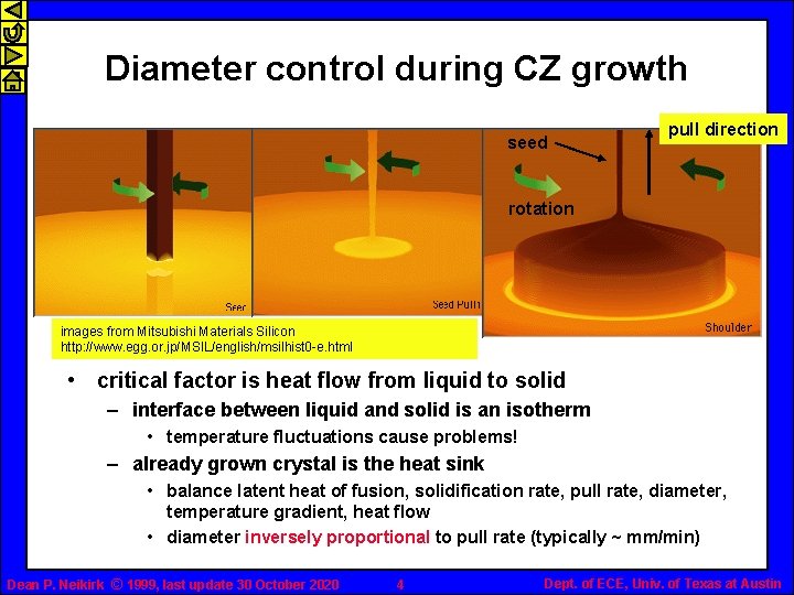
Diameter control during CZ growth seed pull direction rotation images from Mitsubishi Materials Silicon http: //www. egg. or. jp/MSIL/english/msilhist 0 -e. html • critical factor is heat flow from liquid to solid – interface between liquid and solid is an isotherm • temperature fluctuations cause problems! – already grown crystal is the heat sink • balance latent heat of fusion, solidification rate, pull rate, diameter, temperature gradient, heat flow • diameter inversely proportional to pull rate (typically ~ mm/min) Dean P. Neikirk © 1999, last update 30 October 2020 4 Dept. of ECE, Univ. of Texas at Austin
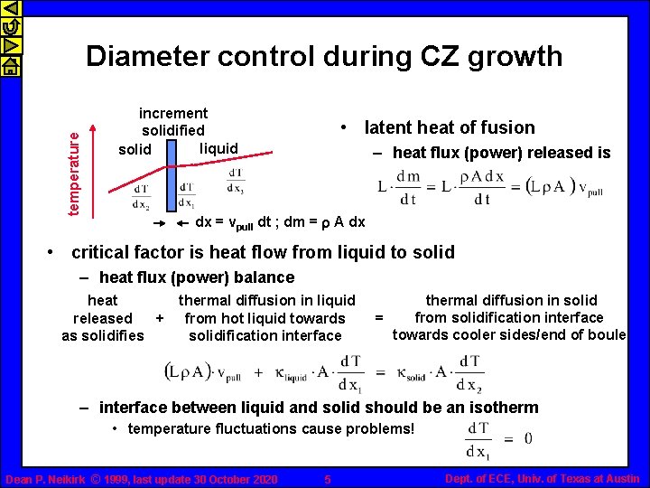
temperature Diameter control during CZ growth increment solidified liquid solid • latent heat of fusion – heat flux (power) released is dx = vpull dt ; dm = r A dx • critical factor is heat flow from liquid to solid – heat flux (power) balance heat thermal diffusion in liquid released + from hot liquid towards as solidifies solidification interface thermal diffusion in solid from solidification interface = towards cooler sides/end of boule – interface between liquid and solid should be an isotherm • temperature fluctuations cause problems! Dean P. Neikirk © 1999, last update 30 October 2020 5 Dept. of ECE, Univ. of Texas at Austin
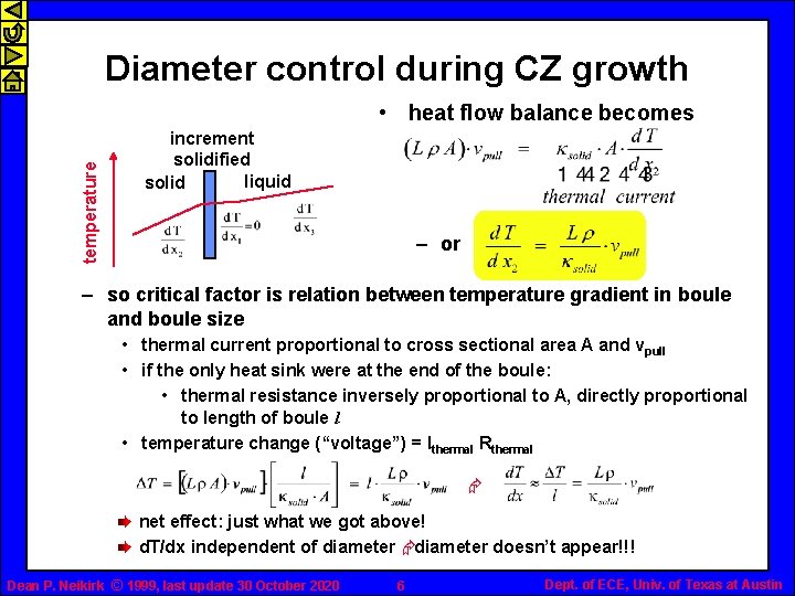
Diameter control during CZ growth temperature • heat flow balance becomes increment solidified liquid solid – or – so critical factor is relation between temperature gradient in boule and boule size • thermal current proportional to cross sectional area A and vpull • if the only heat sink were at the end of the boule: • thermal resistance inversely proportional to A, directly proportional to length of boule l • temperature change (“voltage”) = Ithermal Rthermal Æ net effect: just what we got above! d. T/dx independent of diameter Ædiameter doesn’t appear!!! Dean P. Neikirk © 1999, last update 30 October 2020 6 Dept. of ECE, Univ. of Texas at Austin
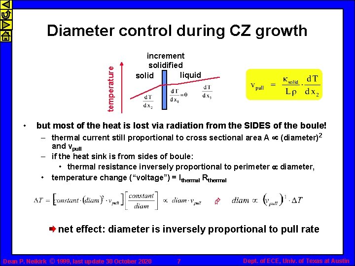
temperature Diameter control during CZ growth • increment solidified liquid solid but most of the heat is lost via radiation from the SIDES of the boule! – thermal current still proportional to cross sectional area A µ (diameter)2 and vpull – if the heat sink is from sides of boule: • thermal resistance inversely proportional to perimeter µ diameter, • temperature change (“voltage”) = Ithermal Rthermal Æ net effect: diameter is inversely proportional to pull rate Dean P. Neikirk © 1999, last update 30 October 2020 7 Dept. of ECE, Univ. of Texas at Austin
Impurities in Czochralski Grown Silicon • choice of crucible material is crucial: – – must be stable at high temperatures (~1500˚ C) carbon: saturates solution and causes poly growth refractories: too much metal in materials quartz: in exclusive use for silicon growth • dissolution of quartz crucibles into melt is major concern: – function of relative velocity between melt & crucible – almost all oxygen present in silicon melt is due to the dissolution of the Si. O 2 crucible – most of this oxygen evaporates in the form of Si. O Dean P. Neikirk © 1999, last update 30 October 2020 8 Dept. of ECE, Univ. of Texas at Austin
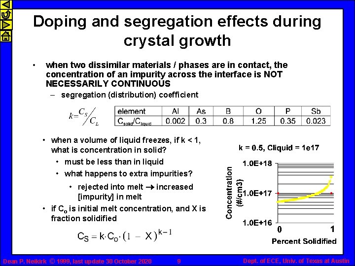
Doping and segregation effects during crystal growth • when two dissimilar materials / phases are in contact, the concentration of an impurity across the interface is NOT NECESSARILY CONTINUOUS – segregation (distribution) coefficient • when a volume of liquid freezes, if k < 1, what is concentration in solid? • must be less than in liquid • what happens to extra impurities? • rejected into melt ® increased [impurity] in melt • if Co is initial melt concentration, and X is fraction solidified 0 Dean P. Neikirk © 1999, last update 30 October 2020 9 1 Dept. of ECE, Univ. of Texas at Austin
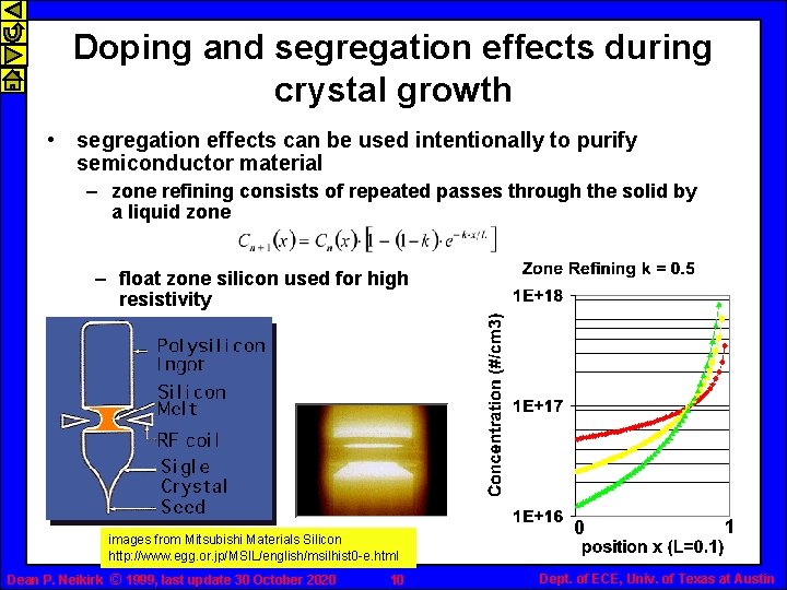
Doping and segregation effects during crystal growth • segregation effects can be used intentionally to purify semiconductor material – zone refining consists of repeated passes through the solid by a liquid zone – float zone silicon used for high resistivity images from Mitsubishi Materials Silicon http: //www. egg. or. jp/MSIL/english/msilhist 0 -e. html Dean P. Neikirk © 1999, last update 30 October 2020 10 0 1 Dept. of ECE, Univ. of Texas at Austin
Oxygen in CZ Silicon • concentrations typically in 1016 - 1018 cm-3 range – segregation coefficient k ~ 1. 25 • more in solid than liquid – contact area between crucible and melt decreases as growth procedes – oxygen content decreases from seed to tang end • effects of oxygen in silicon – ~ 95% interstitial; increases yield strength of silicon via "solution hardening" effect – as-grown crystal is usually supersaturated (occurs above about 6 x 10¹⁷) Dean P. Neikirk © 1999, last update 30 October 2020 11 Dept. of ECE, Univ. of Texas at Austin
Oxygen complexes in silicon • usually donor-like • two classes of complexes: – "old thermal donors" • very small silicon-oxygen atom clusters • very rapid formation rates in 400 -500˚ C range (≥ 1010/cm 3 sec) – "new thermal donors" • slow formation rate above 500˚ C • slow dissolution rate at high temperature – ~1013 cm-3 @ 2 hours, 900˚ C – ~1011 cm-3 @ 2 hours, 1150˚ C • donor behavior possibly due to surface states of large Si. Ox complexes Dean P. Neikirk © 1999, last update 30 October 2020 12 Dept. of ECE, Univ. of Texas at Austin
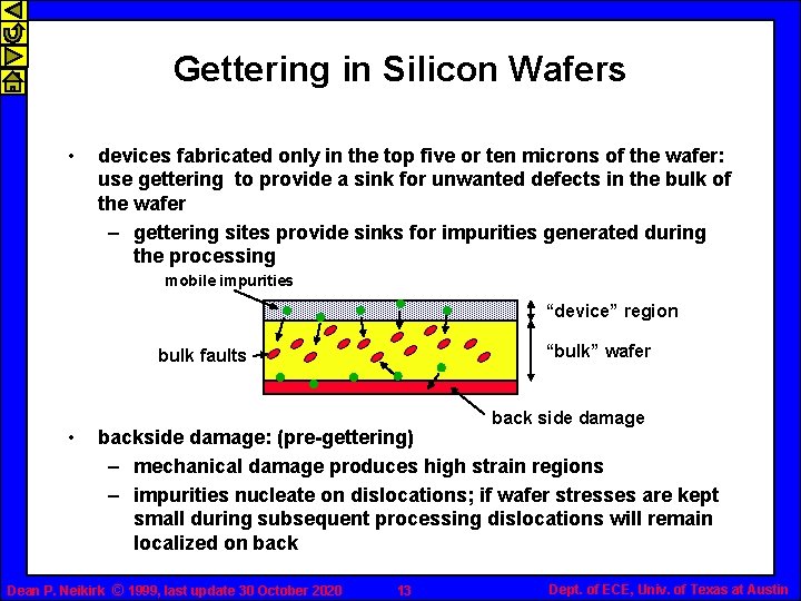
Gettering in Silicon Wafers • devices fabricated only in the top five or ten microns of the wafer: use gettering to provide a sink for unwanted defects in the bulk of the wafer – gettering sites provide sinks for impurities generated during the processing mobile impurities “device” region “bulk” wafer bulk faults • back side damage backside damage: (pre-gettering) – mechanical damage produces high strain regions – impurities nucleate on dislocations; if wafer stresses are kept small during subsequent processing dislocations will remain localized on back Dean P. Neikirk © 1999, last update 30 October 2020 13 Dept. of ECE, Univ. of Texas at Austin
Intrinsic Gettering and Oxygen Precipitates • wafer starting material: – initial oxygen content between ~3. 5 and ~8 x 1017 cm-3 • denuded zone formation: – high temperature step (1050˚ C) reduces interstitial oxygen content via diffusion of O to surface – formation of internal gettering sites: • low temp step (500 -600˚ C) creates large reserve of small, stable oxygen precipitates • higher temperature step (700 -900˚ C) causes growth of larger Si. Ox complexes • subsequent thermal processing creates dislocation loops associated with Si. Ox complexes – actual starting material oxygen concentration and process determined by trial device fab and performance evaluation. Dean P. Neikirk © 1999, last update 30 October 2020 14 Dept. of ECE, Univ. of Texas at Austin
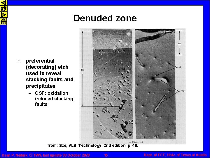
Denuded zone • preferential (decorating) etch used to reveal stacking faults and precipitates – OSF: oxidation induced stacking faults from: Sze, VLSI Technology, 2 nd edition, p. 46. Dean P. Neikirk © 1999, last update 30 October 2020 15 Dept. of ECE, Univ. of Texas at Austin
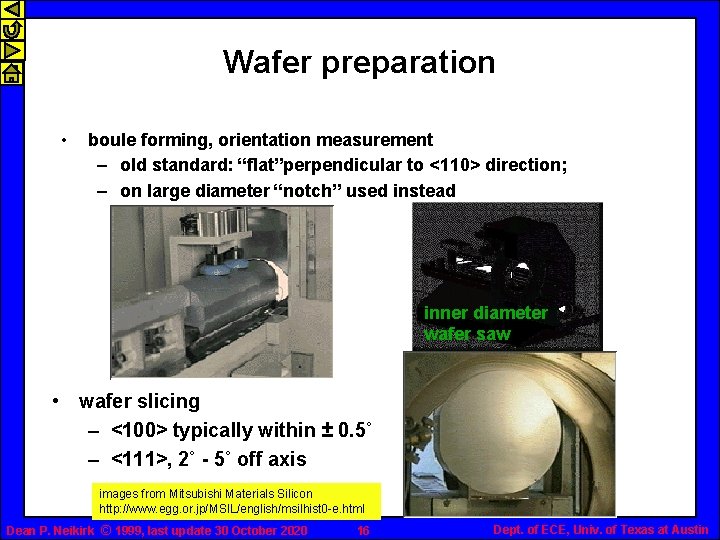
Wafer preparation • boule forming, orientation measurement – old standard: “flat”perpendicular to <110> direction; – on large diameter “notch” used instead inner diameter wafer saw • wafer slicing – <100> typically within ± 0. 5˚ – <111>, 2˚ - 5˚ off axis images from Mitsubishi Materials Silicon http: //www. egg. or. jp/MSIL/english/msilhist 0 -e. html Dean P. Neikirk © 1999, last update 30 October 2020 16 Dept. of ECE, Univ. of Texas at Austin
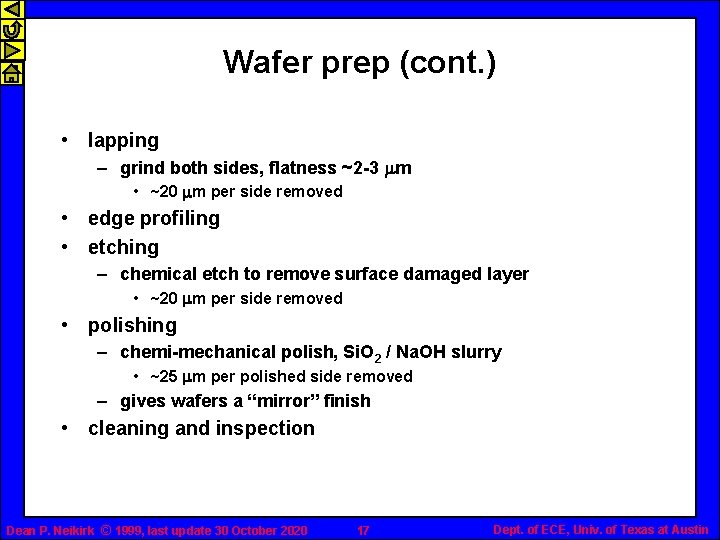
Wafer prep (cont. ) • lapping – grind both sides, flatness ~2 -3 mm • ~20 mm per side removed • edge profiling • etching – chemical etch to remove surface damaged layer • ~20 mm per side removed • polishing – chemi-mechanical polish, Si. O 2 / Na. OH slurry • ~25 mm per polished side removed – gives wafers a “mirror” finish • cleaning and inspection Dean P. Neikirk © 1999, last update 30 October 2020 17 Dept. of ECE, Univ. of Texas at Austin
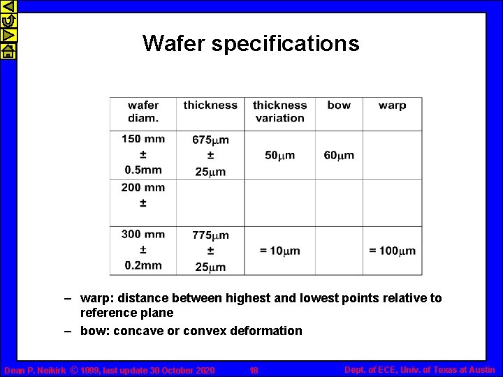
Wafer specifications – warp: distance between highest and lowest points relative to reference plane – bow: concave or convex deformation Dean P. Neikirk © 1999, last update 30 October 2020 18 Dept. of ECE, Univ. of Texas at Austin
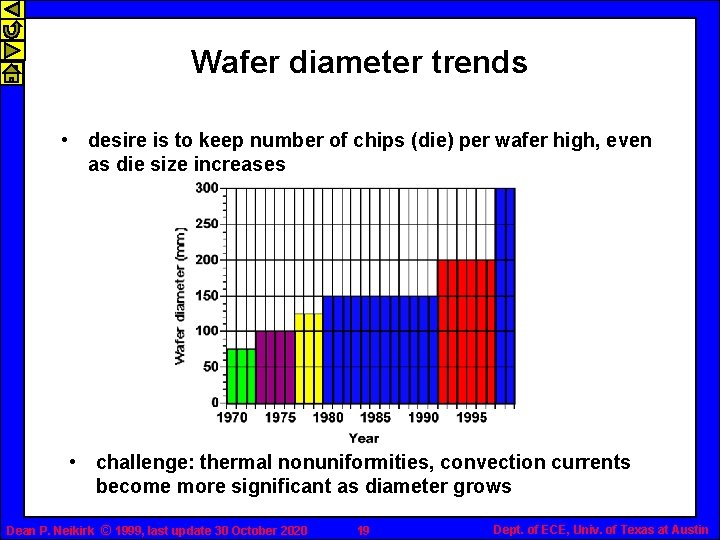
Wafer diameter trends • desire is to keep number of chips (die) per wafer high, even as die size increases • challenge: thermal nonuniformities, convection currents become more significant as diameter grows Dean P. Neikirk © 1999, last update 30 October 2020 19 Dept. of ECE, Univ. of Texas at Austin
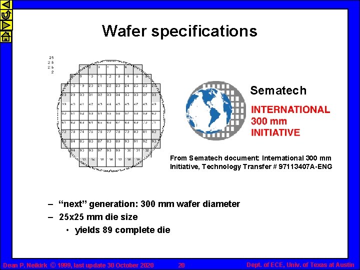
Wafer specifications Sematech From Sematech document: International 300 mm Initiative, Technology Transfer # 97113407 A-ENG – “next” generation: 300 mm wafer diameter – 25 x 25 mm die size • yields 89 complete die Dean P. Neikirk © 1999, last update 30 October 2020 20 Dept. of ECE, Univ. of Texas at Austin

Silicon wafer production • 1999: 4. 263 billion square inches, $5. 883 billion – – $1. 38 per square inch, $0. 21 per square cm 100 mm, 150 mm: 2. 808 billion square inches (65. 9% of total) 200 mm: 1. 441 billion square inches (33. 8%) 300 mm: 0. 014 billion square inches of silicon (0. 3%) • 2000, expected: 4. 692 billion square inches, $6. 475 billion • 2001, expected: 5. 204 billion square inches • 2003, expected: – 200 mm: 2. 892 billion square inches – 300 mm: 0. 112 billion square inches • from EE Times, “Advanced silicon substrates prices rise as wafer glut eases” by J. Robert Lineback Semiconductor Business News (01/12/00, 2: 04 p. m. EST) Dean P. Neikirk © 1999, last update 30 October 2020 21 Dept. of ECE, Univ. of Texas at Austin
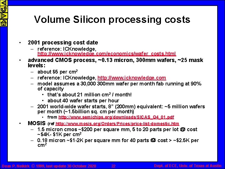
Volume Silicon processing costs • 2001 processing cost date – reference: ICKnowledge, http: //www. icknowledge. com/economics/wafer_costs. html • advanced CMOS process, ~0. 13 micron, 300 mm wafers, ~25 mask levels: – about $5 per cm 2 – reference: ICKnowledge, http: //www. icknowledge. com – model assumes a 30, 000 300 mm wafer per month fab running at 90% of capacity • that’s about 21 million cm 2 / month! • about 40 wafer starts per hour – 2001 world-wide wafer starts, 8” (200 mm) equivalent: ~5 million wafers per month (~1. 5 billion sq. cm per month) • • from http: //www. semichips. org/downloads/SICAS_Q 4_01. pdf MOSIS (ref http: //www. mosis. org/Orders/Prices/price-list-domestic. htm – 1. 5 micron cmos ~$200 per square mm, 5 to 20 parts per lot cost ~$4 K- $1 K per cm 2 – 0. 18 micron ~$1 -2 K per square mm for 40 parts cost > ~$2. 5 K per cm 2 Dean P. Neikirk © 1999, last update 30 October 2020 22 Dept. of ECE, Univ. of Texas at Austin
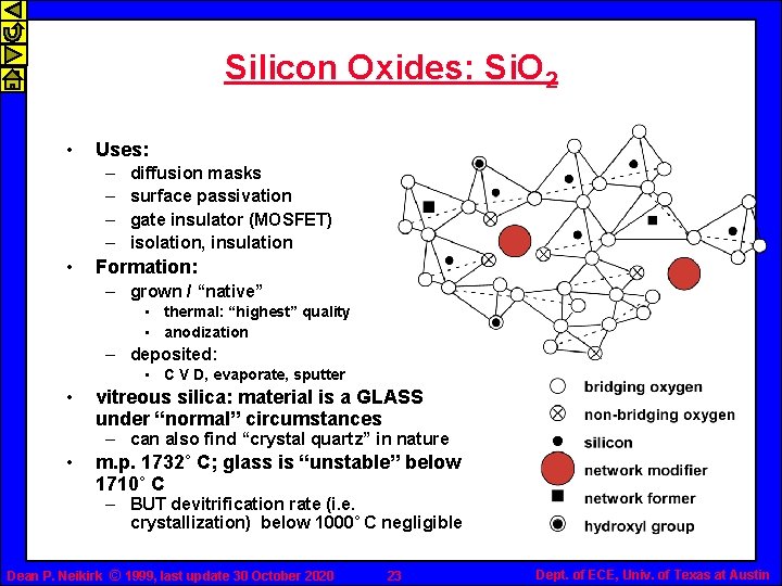
Silicon Oxides: Si. O 2 • Uses: – – • diffusion masks surface passivation gate insulator (MOSFET) isolation, insulation Formation: – grown / “native” • thermal: “highest” quality • anodization – deposited: • C V D, evaporate, sputter • vitreous silica: material is a GLASS under “normal” circumstances – can also find “crystal quartz” in nature • m. p. 1732˚ C; glass is “unstable” below 1710˚ C – BUT devitrification rate (i. e. crystallization) below 1000˚ C negligible Dean P. Neikirk © 1999, last update 30 October 2020 23 Dept. of ECE, Univ. of Texas at Austin
- Slides: 23