Building Pixel Detector Modules in Multi Chip Module
Building Pixel Detector Modules in Multi Chip Module Deposited Technology IEEE Nuclear Science Symposium Roma Oct. 2004 Bergische Universität Wuppertal Peter Gerlach 20. Oct. 2004
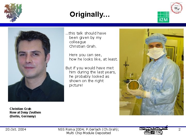
Originally… …this talk should have been given by my colleague Christian Grah. Here you can see, how he looks like, at least. But if you would have met him during the last years, he probably looked as shown on the right picture! Christian Grah Now at Desy Zeuthen (Berlin, Germany) 20. Oct. 2004 NSS Roma 2004; P. Gerlach (Ch. Grah); Multi Chip Module Deposited 2
Subject of this talk Application of a ‘thin’ film technology on a high energy physics detector. Hybrid pixel detector (ATLAS, LHC, CERN) Definition Geometrical constrains Thin film technology Explanation of the process Typical dimensions Introduce some prototypes build, gaining from a strong support of The ATLAS pixel detector project Fraunhofer Institute IZM (Berlin, Germany) Structures realised Results optained Laboratory and test-beam environment Summary (How to…) 20. Oct. 2004 NSS Roma 2004; P. Gerlach (Ch. Grah); Multi Chip Module Deposited 3
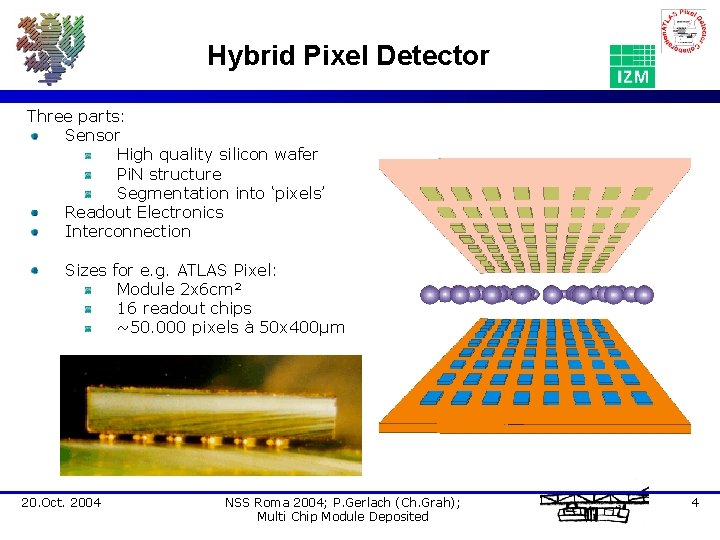
Hybrid Pixel Detector Three parts: Sensor High quality silicon wafer Pi. N structure Segmentation into ‘pixels’ Readout Electronics Interconnection Sizes for e. g. ATLAS Pixel: Module 2 x 6 cm² 16 readout chips ~50. 000 pixels à 50 x 400µm 20. Oct. 2004 NSS Roma 2004; P. Gerlach (Ch. Grah); Multi Chip Module Deposited 4
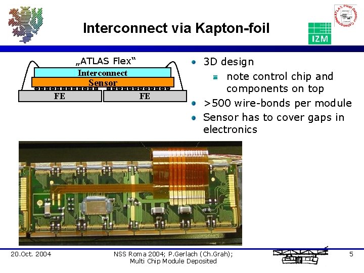
Interconnect via Kapton-foil „ATLAS Flex“ Interconnect Sensor FE 20. Oct. 2004 FE 3 D design note control chip and components on top >500 wire-bonds per module Sensor has to cover gaps in electronics NSS Roma 2004; P. Gerlach (Ch. Grah); Multi Chip Module Deposited 5
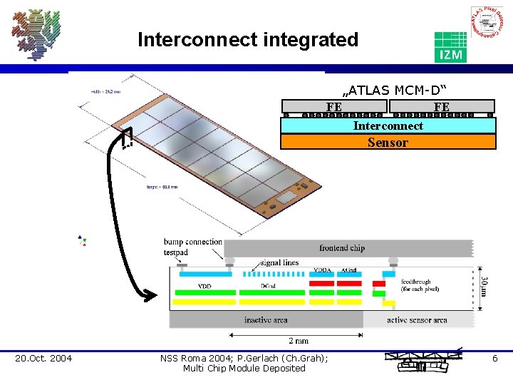
Interconnect integrated „ATLAS MCM-D“ FE FE Interconnect Sensor 20. Oct. 2004 NSS Roma 2004; P. Gerlach (Ch. Grah); Multi Chip Module Deposited 6
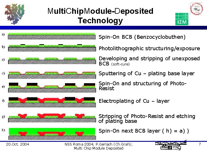
Multi. Chip. Module-Deposited Technology Spin-On BCB (Benzocyclobuthen) Photolithographic structuring/exposure Developing and stripping of unexposed BCB (soft-cure) Sputtering of Cu – plating base layer Spin-On and structuring of Photo. Resist Electroplating of Cu – layer Stripping of Photo-Resist and etching of plating base Spin-On next BCB layer ( h) = a) ) 20. Oct. 2004 NSS Roma 2004; P. Gerlach (Ch. Grah); Multi Chip Module Deposited 7
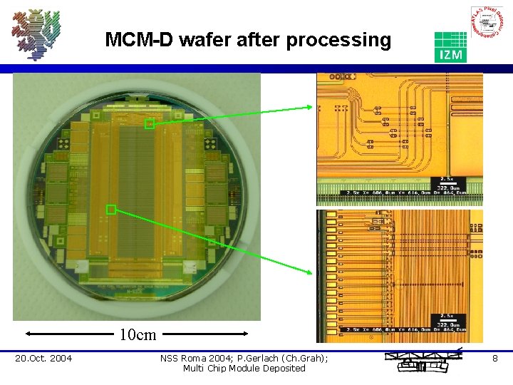
MCM-D wafer after processing 10 cm 20. Oct. 2004 NSS Roma 2004; P. Gerlach (Ch. Grah); Multi Chip Module Deposited 8
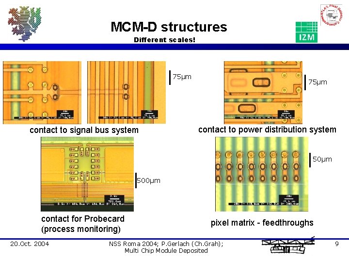
MCM-D structures Different scales! 75µm contact to signal bus system 75µm contact to power distribution system 50µm 500µm contact for Probecard (process monitoring) 20. Oct. 2004 pixel matrix - feedthroughs NSS Roma 2004; P. Gerlach (Ch. Grah); Multi Chip Module Deposited 9
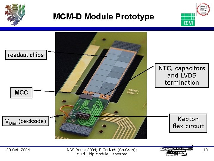
MCM-D Module Prototype readout chips NTC, capacitors and LVDS termination MCC Kapton flex circuit VBias (backside) 20. Oct. 2004 NSS Roma 2004; P. Gerlach (Ch. Grah); Multi Chip Module Deposited 10
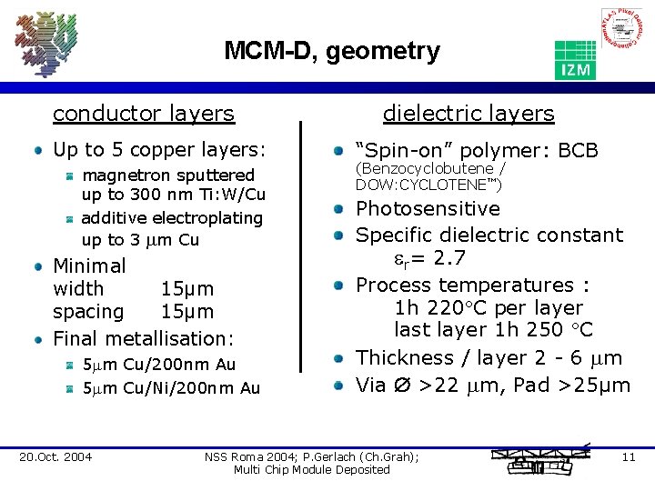
MCM-D, geometry conductor layers Up to 5 copper layers: magnetron sputtered up to 300 nm Ti: W/Cu additive electroplating up to 3 mm Cu Minimal width 15µm spacing 15µm Final metallisation: 5 mm Cu/200 nm Au 5 mm Cu/Ni/200 nm Au 20. Oct. 2004 dielectric layers “Spin-on” polymer: BCB (Benzocyclobutene / DOW: CYCLOTENE™) Photosensitive Specific dielectric constant er= 2. 7 Process temperatures : 1 h 220 C per layer last layer 1 h 250 C Thickness / layer 2 - 6 mm Via >22 mm, Pad >25µm NSS Roma 2004; P. Gerlach (Ch. Grah); Multi Chip Module Deposited 11
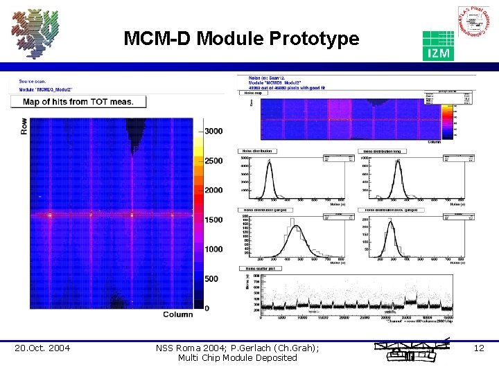
MCM-D Module Prototype 20. Oct. 2004 NSS Roma 2004; P. Gerlach (Ch. Grah); Multi Chip Module Deposited 12
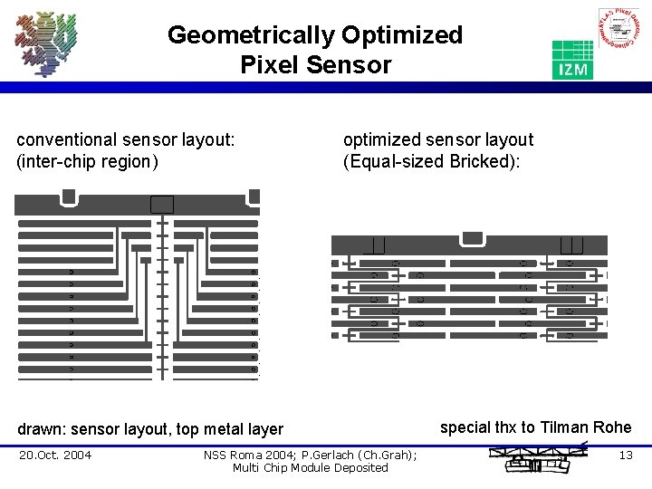
Geometrically Optimized Pixel Sensor conventional sensor layout: (inter-chip region) optimized sensor layout (Equal-sized Bricked): drawn: sensor layout, top metal layer 20. Oct. 2004 NSS Roma 2004; P. Gerlach (Ch. Grah); Multi Chip Module Deposited special thx to Tilman Rohe 13
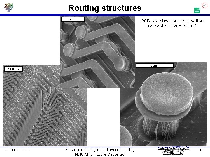
Routing structures 50µm 200µm 20. Oct. 2004 BCB is etched for visualisation (except of some pillars) NSS Roma 2004; P. Gerlach (Ch. Grah); Multi Chip Module Deposited 14
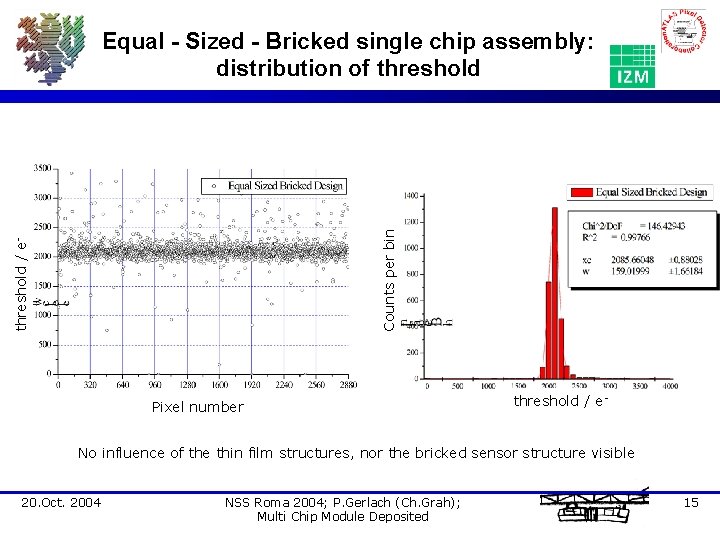
threshold / e- Counts per bin Equal - Sized - Bricked single chip assembly: distribution of threshold Pixel number threshold / e- No influence of the thin film structures, nor the bricked sensor structure visible 20. Oct. 2004 NSS Roma 2004; P. Gerlach (Ch. Grah); Multi Chip Module Deposited 15
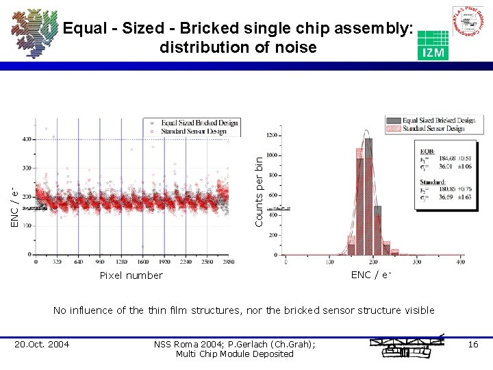
ENC / e- Counts per bin Equal - Sized - Bricked single chip assembly: distribution of noise Pixel number ENC / e- No influence of the thin film structures, nor the bricked sensor structure visible 20. Oct. 2004 NSS Roma 2004; P. Gerlach (Ch. Grah); Multi Chip Module Deposited 16
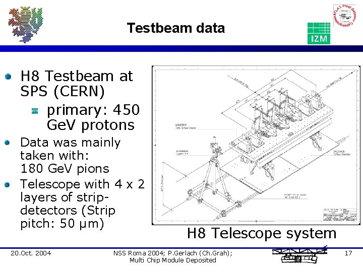
Testbeam data H 8 Testbeam at SPS (CERN) primary: 450 Ge. V protons Data was mainly taken with: 180 Ge. V pions Telescope with 4 x 2 layers of stripdetectors (Strip pitch: 50 µm) 20. Oct. 2004 H 8 Telescope system NSS Roma 2004; P. Gerlach (Ch. Grah); Multi Chip Module Deposited 17
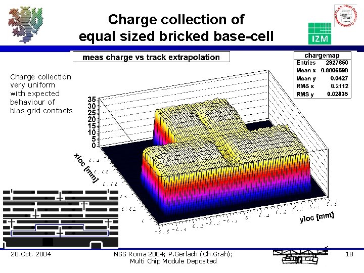
Charge collection of equal sized bricked base-cell Charge collection very uniform with expected behaviour of bias grid contacts 20. Oct. 2004 NSS Roma 2004; P. Gerlach (Ch. Grah); Multi Chip Module Deposited 18
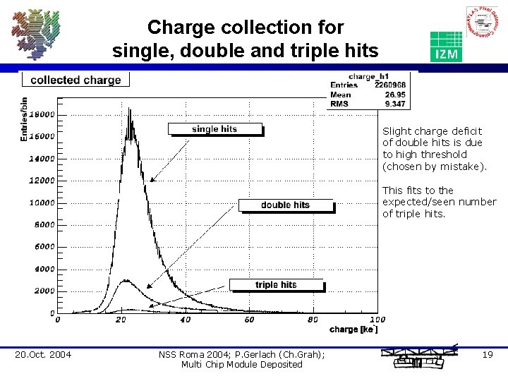
Charge collection for single, double and triple hits Slight charge deficit of double hits is due to high threshold (chosen by mistake). This fits to the expected/seen number of triple hits. 20. Oct. 2004 NSS Roma 2004; P. Gerlach (Ch. Grah); Multi Chip Module Deposited 19
Summary nice higher manageability and better handling of a module bump bonds only (no wire-bonding) sensor cell geometry can be optimized reduced assembly steps rework of full assembled module possible (detach and reattach of chips) options of final metallization (Cu/Cu. Ni/Cu. Au/Cu. Ni. Au/Pb. Sn) allow different technologies higher degree of automation during production Experience with MCMD successfully operated a radhard pixel detector MCMD module performance compatible with Flex modules Cooling ok (chip up design) successfully increased thin film yield defect tolerant design with reduced "critical" area high demand on cleanliness (includes new machinery and optimization of process flow) not so nice increased size (but reduced height) lower testability (reduced access to inter-chip signals) high complexity of the process (find vendor) 20. Oct. 2004 NSS Roma 2004; P. Gerlach (Ch. Grah); Multi Chip Module Deposited 20
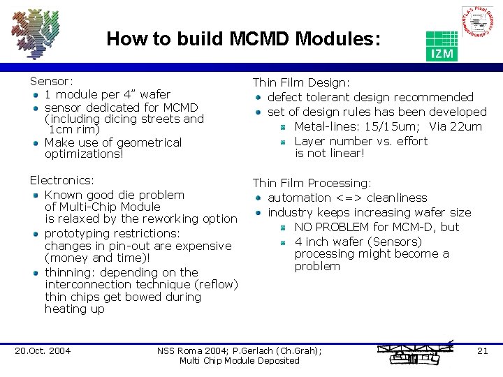
How to build MCMD Modules: Sensor: 1 module per 4” wafer sensor dedicated for MCMD (including dicing streets and 1 cm rim) Make use of geometrical optimizations! Thin Film Design: defect tolerant design recommended set of design rules has been developed Metal-lines: 15/15 um; Via 22 um Layer number vs. effort is not linear! Electronics: Known good die problem of Multi-Chip Module is relaxed by the reworking option prototyping restrictions: changes in pin-out are expensive (money and time)! thinning: depending on the interconnection technique (reflow) thin chips get bowed during heating up Thin Film Processing: automation <=> cleanliness industry keeps increasing wafer size NO PROBLEM for MCM-D, but 4 inch wafer (Sensors) processing might become a problem 20. Oct. 2004 NSS Roma 2004; P. Gerlach (Ch. Grah); Multi Chip Module Deposited 21
- Slides: 21