Building manycore processortoDRAM networks using monolithic silicon photonics
Building manycore processor-to-DRAM networks using monolithic silicon photonics Ajay Joshi†, Christopher Batten†, Vladimir Stojanović†, Krste Asanović‡ †MIT, 77 Massachusetts Ave, Cambridge MA 02139 ‡UC Berkeley, 430 Soda Hall, MC #1776, Berkeley, CA 94720 {joshi, cbatten, vlada}@mit. edu, krste@eecs. berkeley. edu High Performance Embedded Computing (HPEC) Workshop 23 -25 September 2008
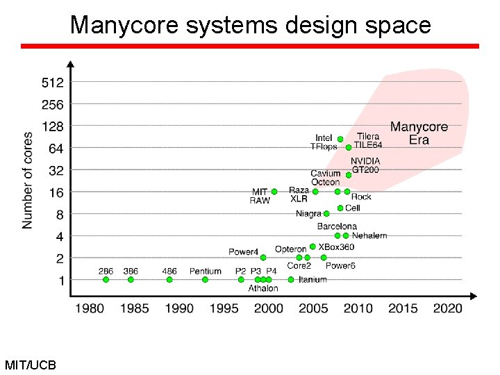
Manycore systems design space MIT/UCB
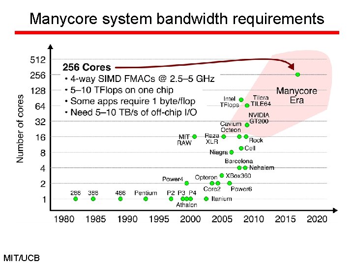
Manycore system bandwidth requirements MIT/UCB

Manycore systems – bandwidth, pin count and power scaling 1 Byte/Flop, 8 Flops/core @ 5 GHz C r rve e S P H & Mobile Client MIT/UCB 4

Interconnect bottlenecks Manycore system cores CPU CPU Interconnect Network Cache MIT/UCB DRAM DIMM Interconnect Network Bottlenecks due to energy and bandwidth density limitations

Interconnect bottlenecks Manycore system cores CPU CPU Interconnect Network Cache MIT/UCB DRAM DIMM Interconnect Network Bottlenecks due to energy and bandwidth density limitations Need to jointly optimize on-chip and off-chip interconnect network
Outline q q q Motivation Monolithic silicon photonic technology Processor-memory network architecture exploration Manycore system using silicon photonics Conclusion MIT/UCB
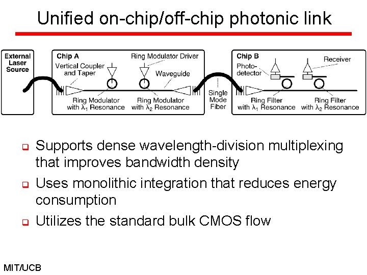
Unified on-chip/off-chip photonic link q q q Supports dense wavelength-division multiplexing that improves bandwidth density Uses monolithic integration that reduces energy consumption Utilizes the standard bulk CMOS flow MIT/UCB

Optical link components 65 nm bulk CMOS chip designed to test various optical devices MIT/UCB

Silicon photonics area and energy advantage Metric Energy (p. J/b) Bandwidth density (Gb/s/μ) Global on-chip photonic link 0. 25 160 -320 Global on-chip optimally repeated electrical link 1 5 Off-chip photonic link (50 μ coupler pitch) 0. 25 13 -26 Off-chip electrical SERDES (100 μ pitch) 5 0. 1 On-chip/off-chip seamless photonic link 0. 25 MIT/UCB

Outline q q q Motivation Monolithic silicon photonic technology Processor-memory network architecture exploration n n q q Baseline electrical mesh topology Electrical mesh with optical global crossbar topology Manycore system using silicon photonics Conclusion MIT/UCB
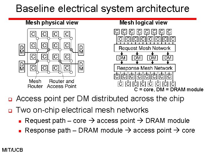
Baseline electrical system architecture Mesh physical view Mesh logical view C = core, DM = DRAM module q q Access point per DM distributed across the chip Two on-chip electrical mesh networks n n MIT/UCB Request path – core access point DRAM module Response path – DRAM module access point core

Interconnect network design methodology q q q Ideal throughput and zero load latency used as design metrics Energy constrained approach is adopted Energy components in a network n n Mesh energy (Em) (router-to-router links (RRL), routers) IO energy (Eio) (logic-to-memory links (LML)) Flit width Calculate on-chip RRL energy Calculate on-chip router energy Calculate mesh throughput MIT/UCB Total energy budget Calculate total mesh energy Calculate energy budget for LML Calculate zero load latency Calculate LML width Calculate I/O throughput

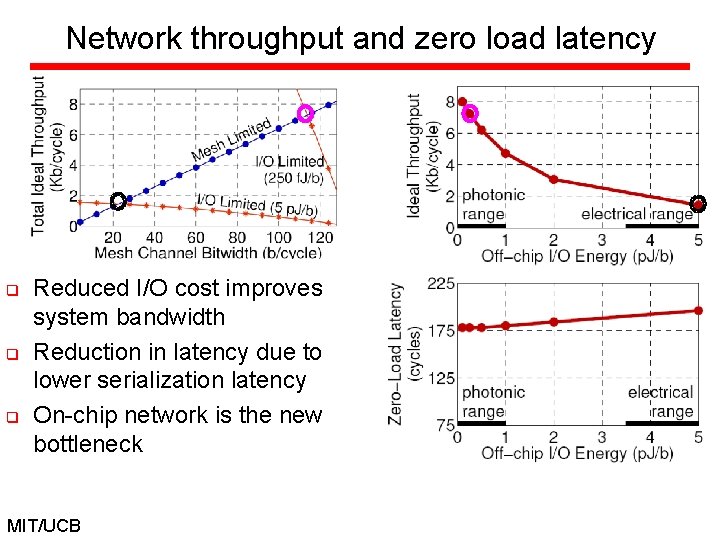
Network throughput and zero load latency (22 nm tech, 256 cores @ 2. 5 GHz, 8 n. J/cyc energy budget) q q q System throughput limited by on-chip mesh or I/O links On-chip mesh could be over-provisioned to overcome mesh bottleneck Zero load latency limited by data serialization MIT/UCB

Network throughput and zero load latency (22 nm tech, 256 cores @ 2. 5 GHz, 8 n. J/cyc energy budget) q q q System throughput limited by on-chip mesh or I/O links On-chip mesh could be over-provisioned to overcome mesh bottleneck Zero load latency limited by data serialization MIT/UCB

OPF: 4 OPF: 2 OPF: 1 Network throughput and zero load latency (22 nm tech, 256 cores @ 2. 5 GHz, 8 n. J/cyc energy budget) q q q System throughput limited by on-chip mesh or I/O links On-chip mesh could be over-provisioned to overcome mesh bottleneck Zero load latency limited by data serialization MIT/UCB
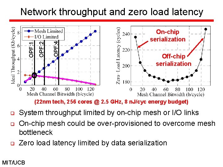
OPF: 4 OPF: 2 OPF: 1 Network throughput and zero load latency On-chip serialization Off-chip serialization (22 nm tech, 256 cores @ 2. 5 GHz, 8 n. J/cyc energy budget) q q q System throughput limited by on-chip mesh or I/O links On-chip mesh could be over-provisioned to overcome mesh bottleneck Zero load latency limited by data serialization MIT/UCB

Outline q q q Motivation Monolithic silicon photonic technology Processor-memory network architecture exploration n n q q Baseline electrical mesh topology Electrical mesh with optical global crossbar topology Manycore system using silicon photonics Conclusion MIT/UCB
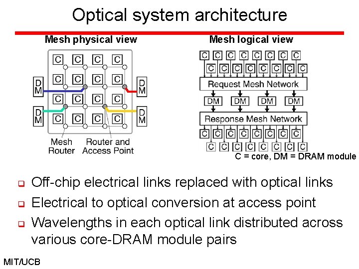
Optical system architecture Mesh physical view Mesh logical view C = core, DM = DRAM module q q q Off-chip electrical links replaced with optical links Electrical to optical conversion at access point Wavelengths in each optical link distributed across various core-DRAM module pairs MIT/UCB

Network throughput and zero load latency q q q Reduced I/O cost improves system bandwidth Reduction in latency due to lower serialization latency On-chip network is the new bottleneck MIT/UCB
Network throughput and zero load latency q q q Reduced I/O cost improves system bandwidth Reduction in latency due to lower serialization latency On-chip network is the new bottleneck MIT/UCB

Optical multi-group system architecture Ci = core in group i, DM = DRAM module, S = global crossbar switch q Break the single on-chip electrical mesh into several groups n n n q q Each group has its own smaller mesh Each group still has one AP for each DM More APs each AP is narrower (uses less λs) Use optical network as a very efficient global crossbar Need a crossbar switch at the memory for arbitration MIT/UCB

Network throughput vs zero load latency Grouping moves traffic from energy-inefficient mesh channels to energyefficient photonic channels q Grouping and silicon photonics provides 10 x 15 x throughput improvement q Grouping reduces ZLL in photonic range, but increases ZLL in electrical range q B 10 x- MIT/UCB 15 x A
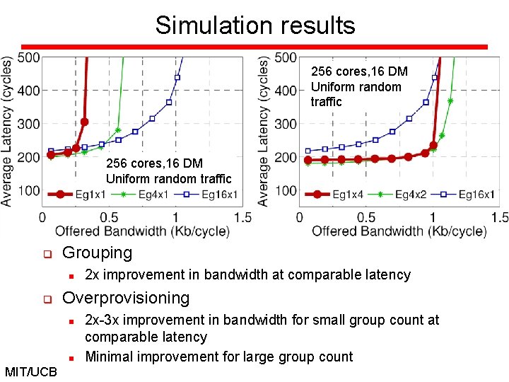
Simulation results 256 cores, 16 DM Uniform random traffic q Grouping n q Overprovisioning n n MIT/UCB 2 x improvement in bandwidth at comparable latency 2 x-3 x improvement in bandwidth for small group count at comparable latency Minimal improvement for large group count

Simulation results 256 cores, 16 DM Uniform random traffic q Replacing off-chip electrical with photonics (Eg 1 x 4 Og 1 x 4) n q 256 cores 16 DM Uniform random traffic 2 x improvement in bandwidth at comparable latency Using opto-electrical global crossbar (Eg 4 x 2 Og 16 x 1) n MIT/UCB 8 x-10 x improvement in bandwidth at comparable latency
Outline q q q Motivation Monolithic silicon photonic technology Processor-memory network architecture exploration Manycore system using silicon photonics Conclusion MIT/UCB

Simplified 16 -core system design MIT/UCB

Simplified 16 -core system design MIT/UCB

Simplified 16 -core system design MIT/UCB

Simplified 16 -core system design MIT/UCB
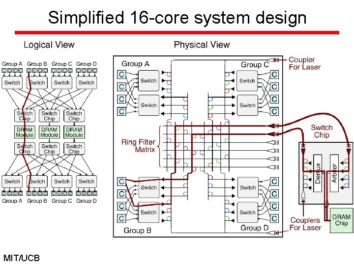
Simplified 16 -core system design MIT/UCB
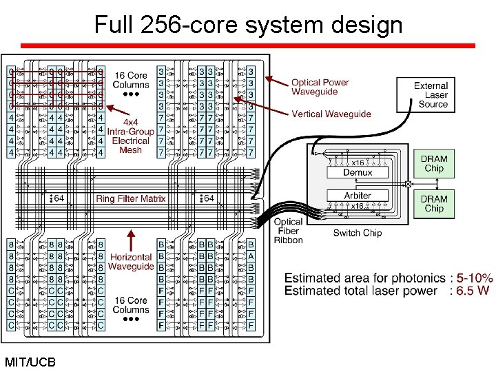
Full 256 -core system design MIT/UCB
Outline q q q Motivation Monolithic silicon photonic technology Processor-memory network architecture exploration Manycore system using silicon photonics Conclusion MIT/UCB

Conclusion q q On-chip network design and memory bandwidth will limit manycore system performance Unified on-chip/off-chip photonic link is proposed to solve this problem Grouping with optical global crossbar improves system throughput For an energy-constrained approach, photonics provide 8 -10 x improvement in throughput at comparable latency MIT/UCB

Backup MIT/UCB
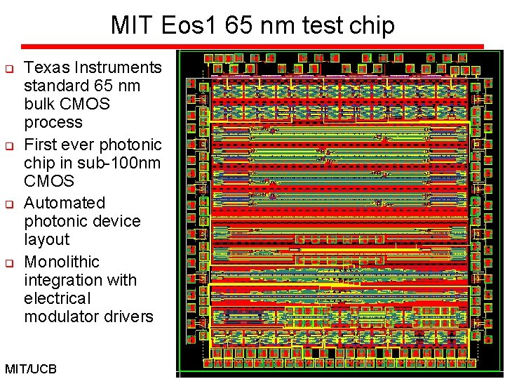
MIT Eos 1 65 nm test chip q q Texas Instruments standard 65 nm bulk CMOS process First ever photonic chip in sub-100 nm CMOS Automated photonic device layout Monolithic integration with electrical modulator drivers MIT/UCB
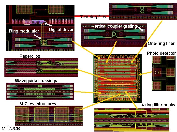
Two-ring filter Ring modulator Digital driver Vertical coupler grating One-ring filter Paperclips Photo detector Waveguide crossings M-Z test structures MIT/UCB 4 ring filter banks
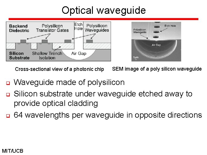
Optical waveguide Cross-sectional view of a photonic chip q q q SEM image of a poly silicon waveguide Waveguide made of polysilicon Silicon substrate under waveguide etched away to provide optical cladding 64 wavelengths per waveguide in opposite directions MIT/UCB
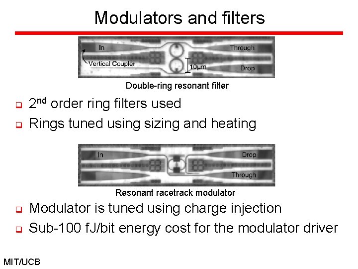
Modulators and filters Double-ring resonant filter q q 2 nd order ring filters used Rings tuned using sizing and heating Resonant racetrack modulator q q Modulator is tuned using charge injection Sub-100 f. J/bit energy cost for the modulator driver MIT/UCB
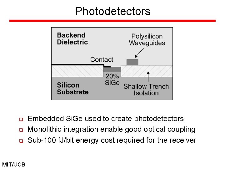
Photodetectors q q q MIT/UCB Embedded Si. Ge used to create photodetectors Monolithic integration enable good optical coupling Sub-100 f. J/bit energy cost required for the receiver
- Slides: 40