Brief Introduction of HighSpeed Circuits for Optical Communication
Brief Introduction of High-Speed Circuits for Optical Communication Systems Zheng Wang Instructor: Dr. Liu
Outline Introduction u System Overview u TIA design u Limiter Design u Frequency Acquisition u CDR Design u Prospects u
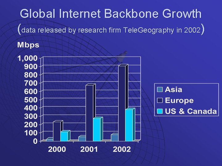
Global Internet Backbone Growth (data released by research firm Tele. Geography in 2002)
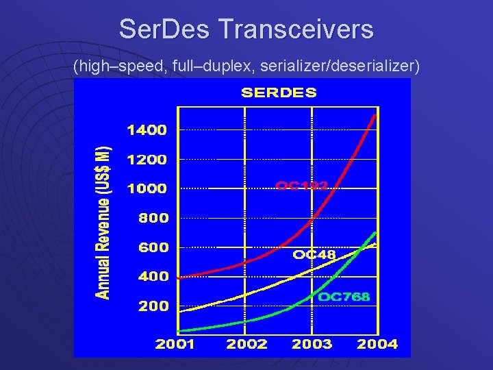
Ser. Des Transceivers (high–speed, full–duplex, serializer/deserializer)
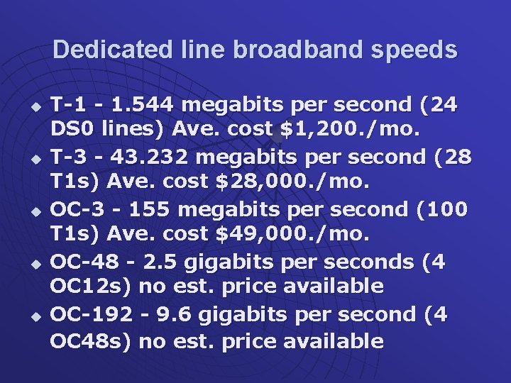
Dedicated line broadband speeds u u u T-1 - 1. 544 megabits per second (24 DS 0 lines) Ave. cost $1, 200. /mo. T-3 - 43. 232 megabits per second (28 T 1 s) Ave. cost $28, 000. /mo. OC-3 - 155 megabits per second (100 T 1 s) Ave. cost $49, 000. /mo. OC-48 - 2. 5 gigabits per seconds (4 OC 12 s) no est. price available OC-192 - 9. 6 gigabits per second (4 OC 48 s) no est. price available
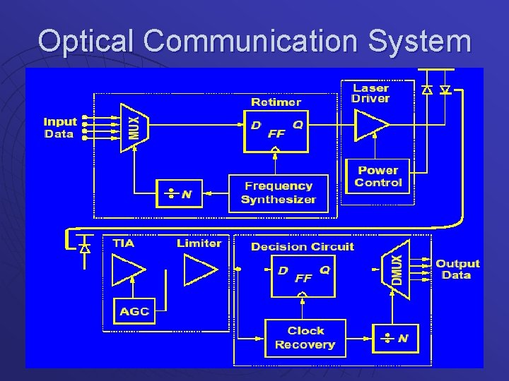
Optical Communication System
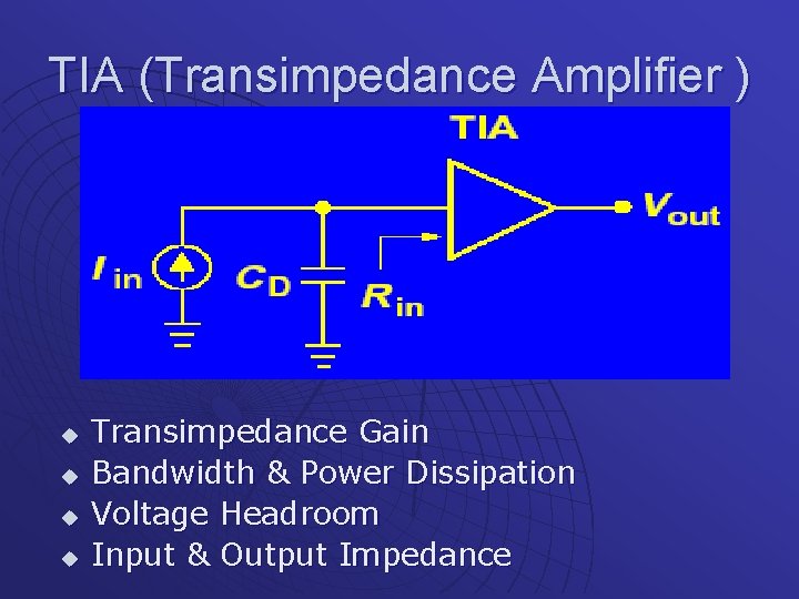
TIA (Transimpedance Amplifier ) u u Transimpedance Gain Bandwidth & Power Dissipation Voltage Headroom Input & Output Impedance
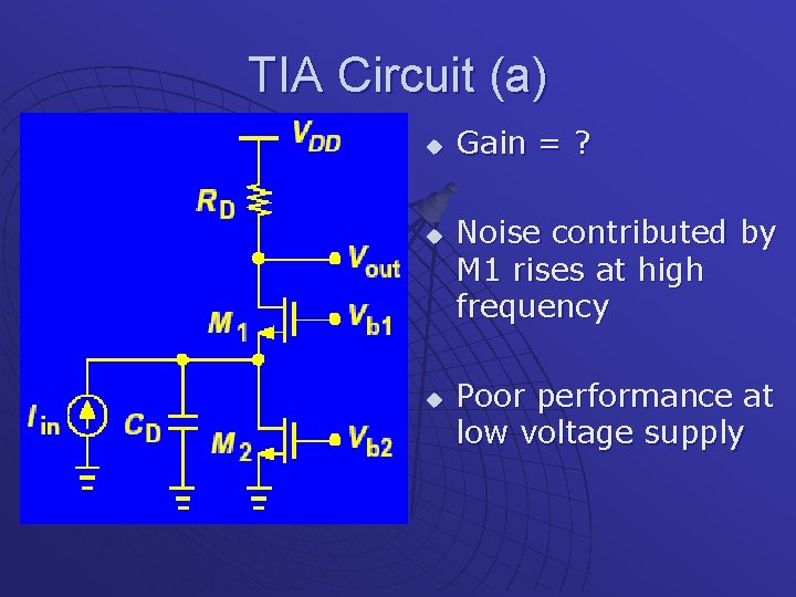
TIA Circuit (a) u u u Gain = ? Noise contributed by M 1 rises at high frequency Poor performance at low voltage supply
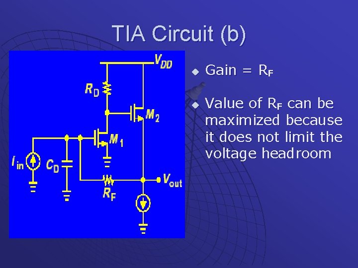
TIA Circuit (b) u u Gain = RF Value of RF can be maximized because it does not limit the voltage headroom
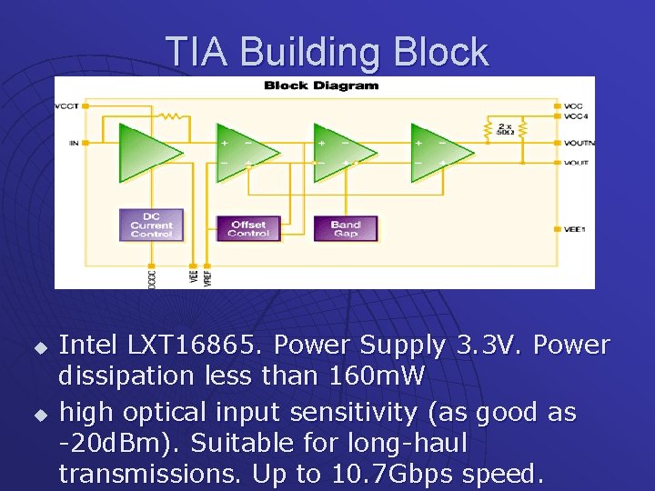
TIA Building Block u u Intel LXT 16865. Power Supply 3. 3 V. Power dissipation less than 160 m. W high optical input sensitivity (as good as -20 d. Bm). Suitable for long-haul transmissions. Up to 10. 7 Gbps speed.
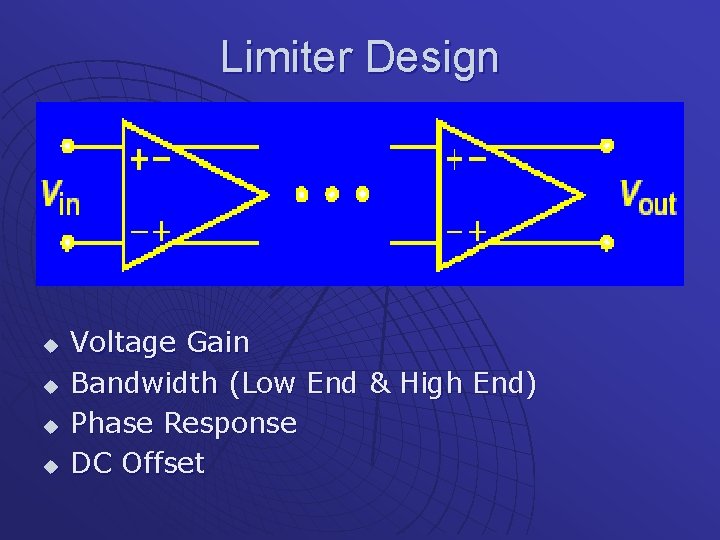
Limiter Design u u Voltage Gain Bandwidth (Low End & High End) Phase Response DC Offset
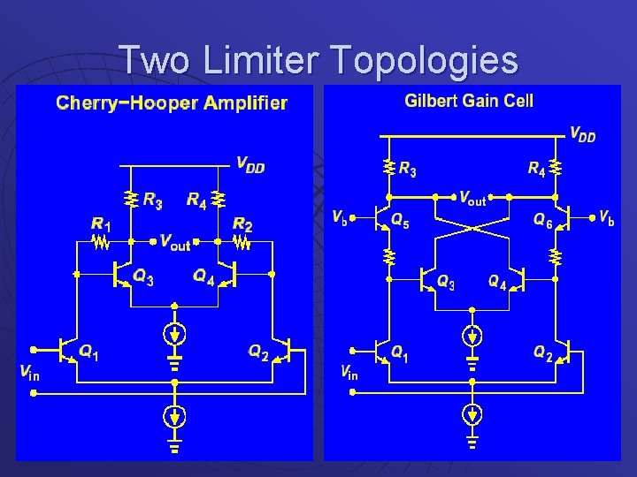
Two Limiter Topologies
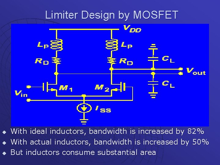
Limiter Design by MOSFET u u u With ideal inductors, bandwidth is increased by 82% With actual inductors, bandwidth is increased by 50% But inductors consume substantial area
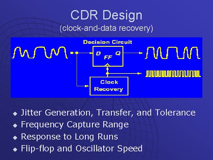
CDR Design (clock-and-data recovery) u u Jitter Generation, Transfer, and Tolerance Frequency Capture Range Response to Long Runs Flip-flop and Oscillator Speed
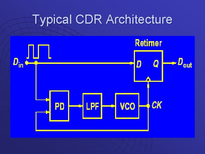
Typical CDR Architecture
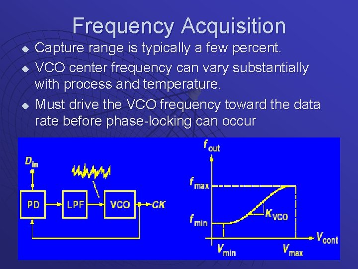
Frequency Acquisition u u u Capture range is typically a few percent. VCO center frequency can vary substantially with process and temperature. Must drive the VCO frequency toward the data rate before phase-locking can occur
Definition of Jitter Synchronous networks such as the Synchronous Digital Hierarchy (SDH) and the Synchronous Optical NETwork (SONET) rely on highly accurate and stable synchronization to process data in and out of network elements. u Jitter is used to describe short term, noncumulative variations of the significant instants of a digital signal from their ideal positions in time u
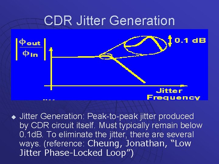
CDR Jitter Generation u Jitter Generation: Peak-to-peak jitter produced by CDR circuit itself. Must typically remain below 0. 1 d. B. To eliminate the jitter, there are several ways. (reference: Cheung, Jonathan, “Low Jitter Phase-Locked Loop”)
Prospects of CMOS Technology u u u u The transit frequency of 0. 13 -um NMOS devices exceeds 100 GHz. As with RF circuits, optical communication circuits can greatly benefit from CMOS technology. The cost and integration advantages of CMOS manifest themselves in: - Wave-Division Multiplexing Systems - Multiple Transceivers for Bundle of Fibers - Highly-Integrated Transceivers CMOS at 40 Gb/s? Why Not?
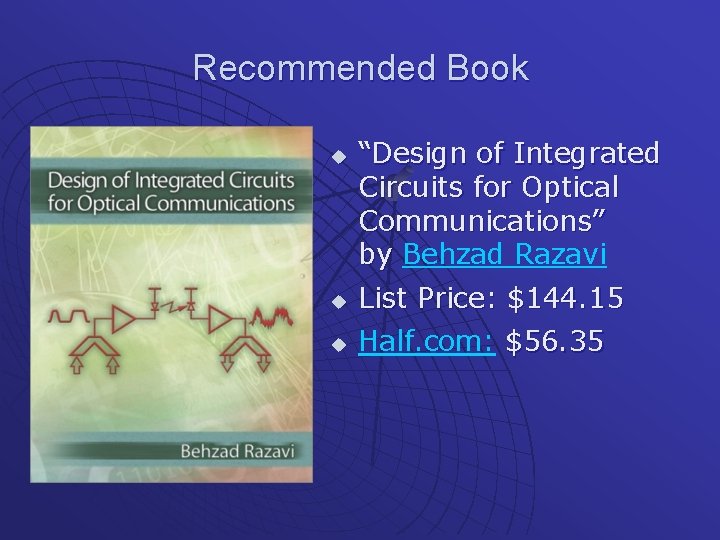
Recommended Book u “Design of Integrated Circuits for Optical Communications” by Behzad Razavi u List Price: $144. 15 u Half. com: $56. 35
Reference Paper u u u Cheung, Jonathan, “Low Jitter Phase-Locked Loop” “LXT 16865 Transimpedance Amplifier (TIA)” http: //www. intel. com/design/network/products/optical/phys/lxt 16865. htm Mauldin, Alan, “Global Internet Backbone Growth Slows Dramatically, ” October 16, 2002 October 21, 2003 http: //www. telegeography. com/press/releases/2002/16 -oct-2002. html Schmitt, Nicolas, “Jitter Measurements of Agilent Technologies OC-48 Optical Transceivers using the Omni. BER 718” http: //ftp. agilent. com/pub/semiconductor/morpheus/docs/jitter_measure ments 2. pdf “T 1, T 3, OC 12, OC 48 and OC 192 Research Information” http: //www. broadband-internet-provider. com/research-information. htm

Thank You for your time Questions?
- Slides: 22