Booster Cogging Teststand Progress Update Kiyomi Seiya Alex

Booster Cogging Teststand Progress Update Kiyomi Seiya, Alex Waller, Craig Drennan August 22, 2012
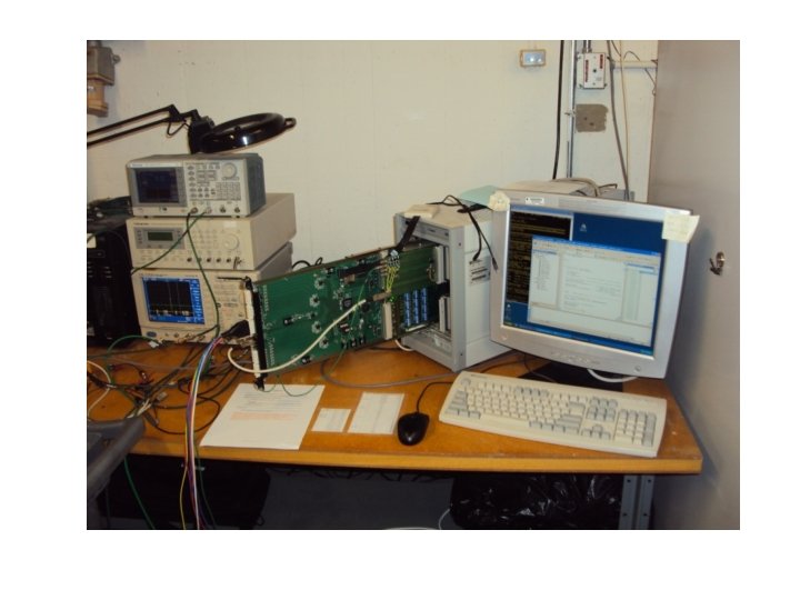

MFC VXI Module provided by the AD/ RF Group.
 – Management of VXI")
Task Outline • Development of front-end, slot 0, processor. (Alex) – Management of VXI Modules. – ACNET interface for Cogging parameter and curve management. • Development of DSP and FPGA firmware. (Craig) – Management of parameters and curves in Flash memory and in active controller registers. – Establish application specific logic and sampling clocks and data transfer settings. – Establish application specific I/O connections and interfaces.
 • Development and testing of cogging method, algorithm, controller. (Kiyomi)")
Task Outline (cont. ) • Development and testing of cogging method, algorithm, controller. (Kiyomi) – Establish a method for doing the magnetic cogging. – Determine the controller algorithm, structure, and operator programmable parameters and curves. – Build and test the controller firmware/software on the bench. – Establish connections to the Booster LLRF controls for testing with beam. – Perform testing and commissioning of new magnetic cogging.

Progress on Slot 0 Front-End • Adopted the full VXI Resource Manager – Manages module memory allocation and statically and dynamically allocated address offsets. • Brought the Cogging development test stand online using the MVME 2434. – MVME 2434 is currently used in AD/RF applications. – Adopted library of Slot 0 software routines for configuring and testing the MFC module. – Establish and tested network and boot settings.
 • Updating Slot 0 Processor for Booster")
Progress on Slot 0 Front-End (cont. ) • Updating Slot 0 Processor for Booster LLRF – Cogging and other LLRF VXI controls will employ the MVME 5500 and Vx. Works 6. 4. – First Booster MVME 5500 node was brought online earlier this month. – Then new processor has its own ACNET node (BSTRTS) and Booster Slot 0 routines are successfully running on this node.

Progress on DSP and FPGA Firmware • Got up to speed with MFC module capabilities and functions. – VXI/VME interface including VXI configuration Registers. – DSP intialization of clock distribution, analog I/O, external memory interfaces, and on board serial interfaces. – Structure and function of interrupt service routines and CPLD state machines for data bus negotiation and data transfer. – Learned to load FPGA and DSP code over the network using the Slot 0 controller. – Procured and put into service the JTAG DSP in circuit emulator.
 • Started establishing the application specific module configuration.")
DSP and FPGA Firmware (cont. ) • Started establishing the application specific module configuration. – Started Writing new C routines for the DSP for managing operator programmable parameters and curves. – Have written application specific documents for setting up clocks for sampling and FPGA logic. – Started a document, along with FPGA code, for establishing a memory map for the programmable parameters and curves. – Started a document to record DSP external memory interface settings

Progress on Cogging Controller • See Kiyomi’s slides from the July 11 th PIP meeting. – \beamssrv 1pip. bdPublicMeetingsPIP_July 11_2012. pptx • A general method for magnetic cogging using the Booster dipole correctors has been established. • Feasibility tests on Booster beam using the correctors have been made.
- Slides: 10