Bipolar Transistors Chapter 21 Introduction An Overview of
Bipolar Transistors Chapter 21 § Introduction § An Overview of Bipolar Transistors § Bipolar Transistor Operation § Bipolar Transistor Characteristics § Summary of Bipolar Transistor Characteristics § Bipolar Transistor Amplifiers § Other Bipolar Transistor Applications Storey: Electrical & Electronic Systems © Pearson Education Limited 2004 OHT 21. 1
Introduction 21. 1 § Bipolar transistors are one of the main ‘building-blocks’ in electronic systems § They are used in both analogue and digital circuits § They incorporate two pn junctions and are sometimes known as bipolar junction transistors or BJTs § Here will refer to them simply as bipolar transistors Storey: Electrical & Electronic Systems © Pearson Education Limited 2004 OHT 21. 2
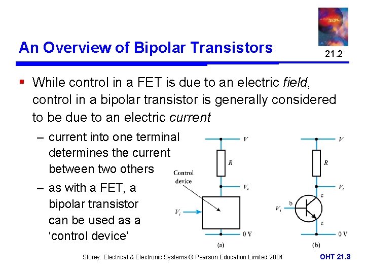
An Overview of Bipolar Transistors 21. 2 § While control in a FET is due to an electric field, control in a bipolar transistor is generally considered to be due to an electric current – current into one terminal determines the current between two others – as with a FET, a bipolar transistor can be used as a ‘control device’ Storey: Electrical & Electronic Systems © Pearson Education Limited 2004 OHT 21. 3
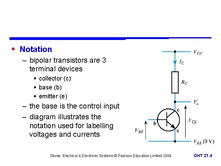
§ Notation – bipolar transistors are 3 terminal devices § collector (c) § base (b) § emitter (e) – the base is the control input – diagram illustrates the notation used for labelling voltages and currents Storey: Electrical & Electronic Systems © Pearson Education Limited 2004 OHT 21. 4

§ Relationship between the collector current and the base current in a bipolar transistor – characteristic is approximately linear – magnitude of collector current is generally many times that of the base current – the device provides current gain Storey: Electrical & Electronic Systems © Pearson Education Limited 2004 OHT 21. 5

§ Construction – two polarities: npn and pnp Storey: Electrical & Electronic Systems © Pearson Education Limited 2004 OHT 21. 6
Bipolar Transistor Operation 21. 3 § We will consider npn transistors – pnp devices are similar but with different polarities of voltage and currents – when using npn transistors § collector is normally more positive than the emitter § VCE might be a few volts § device resembles two back-to-back diodes – but has very different characteristics § with the base open-circuit negligible current flows from the collector to the emitter Storey: Electrical & Electronic Systems © Pearson Education Limited 2004 OHT 21. 7
§ Now consider what happens when a positive voltage is applied to the base (with respect to the emitter) – this forward biases the base-emitter junction – the base region is light doped and very thin – because it is likely doped, the current produced is mainly electrons flowing from the emitter to the base – because the base region is thin, most of the electrons entering the base get swept across the base-collector junction into the collector – this produces a collector current that is much larger than the base current – this gives current amplification Storey: Electrical & Electronic Systems © Pearson Education Limited 2004 OHT 21. 8

§ Transistor action Storey: Electrical & Electronic Systems © Pearson Education Limited 2004 OHT 21. 9
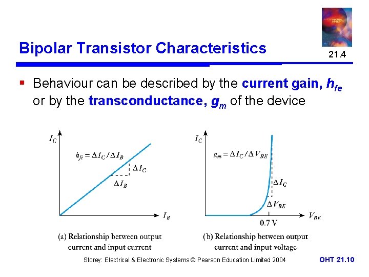
Bipolar Transistor Characteristics 21. 4 § Behaviour can be described by the current gain, hfe or by the transconductance, gm of the device Storey: Electrical & Electronic Systems © Pearson Education Limited 2004 OHT 21. 10
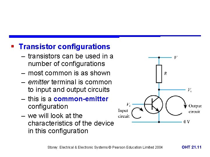
§ Transistor configurations – transistors can be used in a number of configurations – most common is as shown – emitter terminal is common to input and output circuits – this is a common-emitter configuration – we will look at the characteristics of the device in this configuration Storey: Electrical & Electronic Systems © Pearson Education Limited 2004 OHT 21. 11
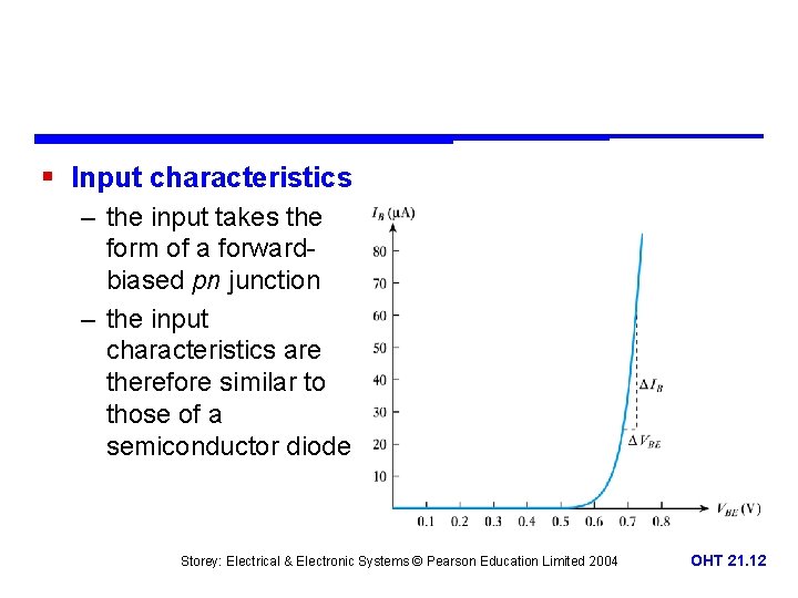
§ Input characteristics – the input takes the form of a forwardbiased pn junction – the input characteristics are therefore similar to those of a semiconductor diode Storey: Electrical & Electronic Systems © Pearson Education Limited 2004 OHT 21. 12
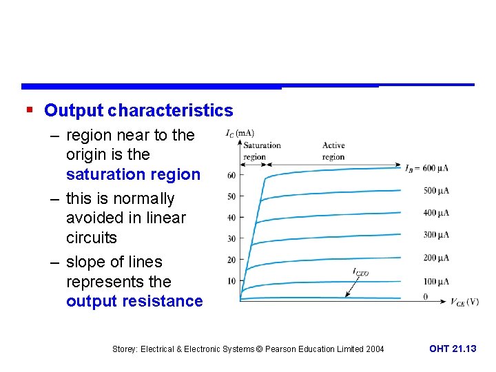
§ Output characteristics – region near to the origin is the saturation region – this is normally avoided in linear circuits – slope of lines represents the output resistance Storey: Electrical & Electronic Systems © Pearson Education Limited 2004 OHT 21. 13
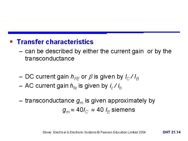
§ Transfer characteristics – can be described by either the current gain or by the transconductance – DC current gain h. FE or is given by IC / IB – AC current gain hfe is given by ic / ib – transconductance gm is given approximately by gm 40 IC 40 IE siemens Storey: Electrical & Electronic Systems © Pearson Education Limited 2004 OHT 21. 14

§ Equivalent circuits for a bipolar transistor Storey: Electrical & Electronic Systems © Pearson Education Limited 2004 OHT 21. 15
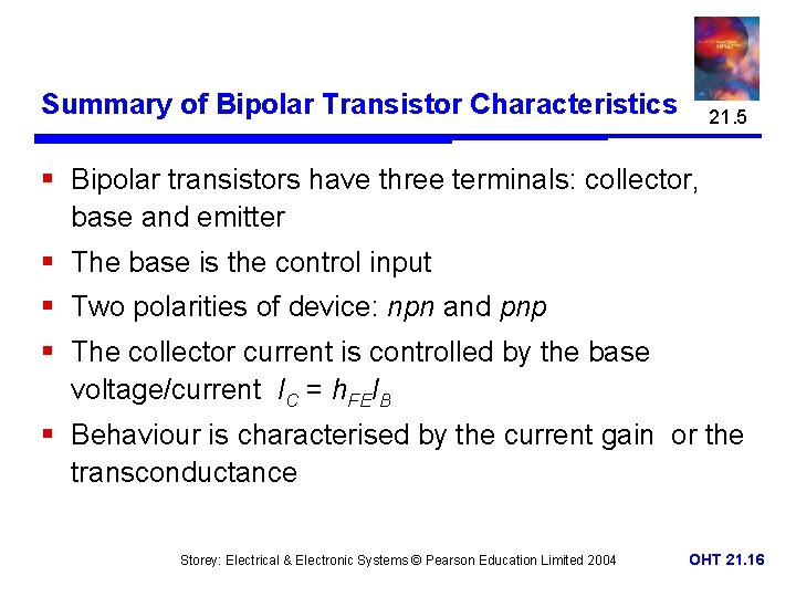
Summary of Bipolar Transistor Characteristics 21. 5 § Bipolar transistors have three terminals: collector, base and emitter § The base is the control input § Two polarities of device: npn and pnp § The collector current is controlled by the base voltage/current IC = h. FEIB § Behaviour is characterised by the current gain or the transconductance Storey: Electrical & Electronic Systems © Pearson Education Limited 2004 OHT 21. 16
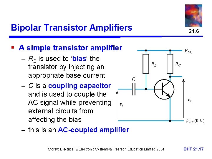
Bipolar Transistor Amplifiers 21. 6 § A simple transistor amplifier – RB is used to ‘bias’ the transistor by injecting an appropriate base current – C is a coupling capacitor and is used to couple the AC signal while preventing external circuits from affecting the bias – this is an AC-coupled amplifier Storey: Electrical & Electronic Systems © Pearson Education Limited 2004 OHT 21. 17
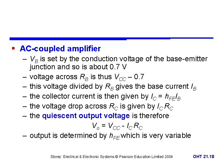
§ AC-coupled amplifier – VB is set by the conduction voltage of the base-emitter junction and so is about 0. 7 V – voltage across RB is thus VCC – 0. 7 – this voltage divided by RB gives the base current IB – the collector current is then given by IC = h. FEIB – the voltage drop across RC is given by IC RC – the quiescent output voltage is therefore Vo = VCC - IC RC – output is determined by h. FE which is very variable Storey: Electrical & Electronic Systems © Pearson Education Limited 2004 OHT 21. 18
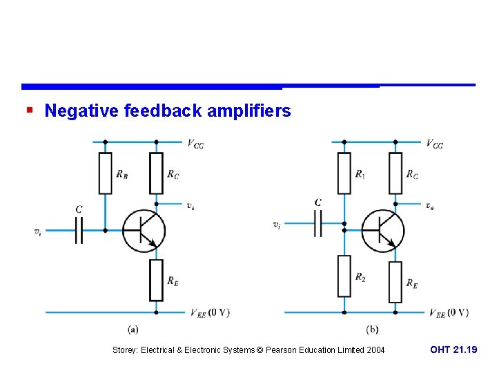
§ Negative feedback amplifiers Storey: Electrical & Electronic Systems © Pearson Education Limited 2004 OHT 21. 19
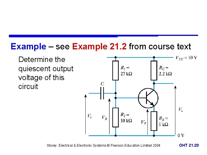
Example – see Example 21. 2 from course text Determine the quiescent output voltage of this circuit Storey: Electrical & Electronic Systems © Pearson Education Limited 2004 OHT 21. 20

Base current is small, so Emitter voltage VE = VB – VBE = 2. 7 – 0. 7 = 2. 0 V Emitter current Since IB is small, collector current IC IE = 2 m. A Output voltage = VCC – ICRC = 10 - 2 m. A 2. 2 k = 5. 6 V Storey: Electrical & Electronic Systems © Pearson Education Limited 2004 OHT 21. 21
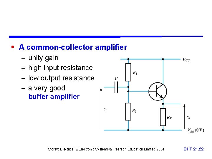
§ A common-collector amplifier – – unity gain high input resistance low output resistance a very good buffer amplifier Storey: Electrical & Electronic Systems © Pearson Education Limited 2004 OHT 21. 22

Other Bipolar Transistor Applications 21. 7 § A phase splitter Storey: Electrical & Electronic Systems © Pearson Education Limited 2004 OHT 21. 23
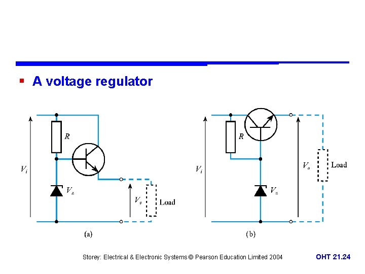
§ A voltage regulator Storey: Electrical & Electronic Systems © Pearson Education Limited 2004 OHT 21. 24
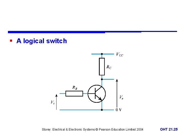
§ A logical switch Storey: Electrical & Electronic Systems © Pearson Education Limited 2004 OHT 21. 25
Key Points § Bipolar transistors are widely used in both analogue and digital circuits § They can be considered as either voltage-controlled or current-controlled devices § Their characteristics may be described by their gain or by their transconductance § Feedback can be used to overcome problems of variability § The majority of circuits use transistors in a common-emitter configuration where the input is applied to the base and the output is taken from the collector § Common-collector circuits make good buffer amplifiers § Bipolar transistors are used in a wide range of applications Storey: Electrical & Electronic Systems © Pearson Education Limited 2004 OHT 21. 26
- Slides: 26