Bipolar Transistor Second Order Effects In this lecture

Bipolar Transistor : Second Order Effects

In this lecture, you will learn about the following second order effects in the bipolar transistor • current crowding • base width modulation (Early effect) • punch-through and avalanche breakdown • high level injection Read : 1. Neamen, “Semiconductor Physics and Devices”, 3 rd Edition, Mc. Graw. Hill (2003), pp. 397 -413. 2. Muller, Kamins and Chan, “Device Electronics for Integrated Circuits”, 3 rd Edition, Wiley (2003), pp. 324 -331.

Fig. 1: Cross-section of an n-p-n bipolar transistor showing the base current distribution

Fig. 2: 2 -D vector plot of the currents from a simulation of a bipolar transistor using MEDICI.
 top view, and (b) cross-sectional view, of a bipolar transistor showing")
Fig. 3: (a) top view, and (b) cross-sectional view, of a bipolar transistor showing the interdigitated emitter and base structure.

Fig. 4: Output characteristics of a bipolar transistor showing significant basewidth modulation effect.

Fig. 5: Illustration of the change in the gradient of the minority carrier conc. profile in the base as a result of the change in the neutral base width.

Fig. 6: Output characteristics of the bipolar transistor showing the Early voltage

Fig. 7: Schematic diagram showing punch-through of the base in a bipolar transistor.
 in equilibrium, (b) at")
Fig. 8: Energy band diagram of a bipolar transistor (a) in equilibrium, (b) at punch-through.
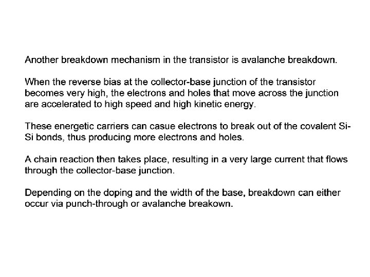
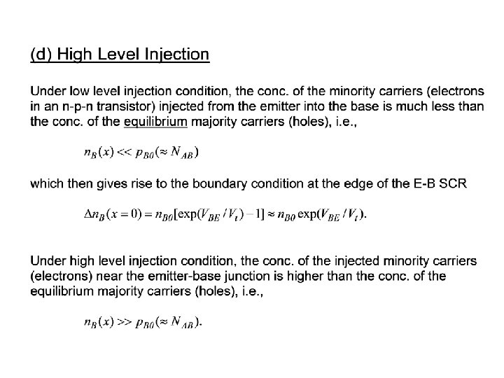

Fig. 9 : Electron and hole conc. Profiles in the base under low level injection (solid lines) and high level injection (dashed lines) conditions.

Fig 10 : Gummel plot for a bipolar transistor Fig. 11 : Plot of versus IC
- Slides: 14