Bipolar junction transistors History The transistor was probably

Bipolar junction transistors

History The transistor was probably the most important invention of the 20 th Century. Reference: Bell Labs Museum B. G. Streetman & S. Banerjee ‘Solid State Electronic Devices’, Prentice Hall 1999.

Point-Contact Transistor – first transistor ever made

Introduction • • • The basic of electronic system nowadays is semiconductor device. The famous and commonly use of this device is BJTs (Bipolar Junction Transistors). It can be use as amplifier and logic switches. BJT consists of three terminal: – collector : C – base : B – emitter : E • Two types of BJT : pnp and npn

Transistor construction • 3 layer semiconductor device consisting: – 2 n- and 1 p-type layers of material npn transistor – 2 p- and 1 n-type layers of material pnp transistor • The term bipolar reflects the fact that holes and electrons participate in the injection process into the oppositely polarized material • A single pn junction has two different types of bias: – forward bias – reverse bias

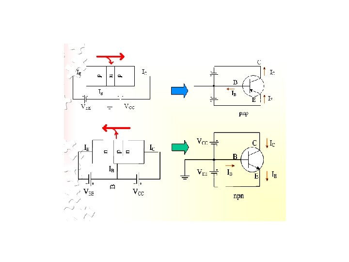
Position of the terminals and symbols of BJT • Base is located at the middle and more thin from the level of collector and emitter • The emitter and collector terminals are made of the same type of semiconductor material, while the base of the other type of material

Transistor currents -The arrow is always drawn on the emitter -The arrow always point toward the n-type IC=the collector current IB= the base current IE= the emitter current -The arrow indicates the direction of the emitter current: pnp: E B npn: B E

• By imaging the analogy of diode, transistor can be construct like two diodes that connetecd together. • It can be conclude that the work of transistor is based on work of diode.

Transistor operation • The basic operation will be described using the pnp transistor. The operation of the pnp transistor is exactly the same if the roles played by the electron and hole are interchanged. • One p-n junction of a transistor is reverse-biased, whereas the other is forward-biased. Forward-biased junction of a pnp transistor Reverse-biased junction of a pnp transistor

• Both biasing potentials have been applied to a pnp transistor and resulting majority and minority carrier flows indicated. • Majority carriers (+) will diffuse across the forwardbiased p-n junction into the n-type material. • A very small number of carriers (+) will through n-type material to the base terminal. Resulting IB is typically in order of microamperes. • The large number of majority carriers will diffuse across the reverse-biased junction into the p-type material connected to the collector terminal.

• Majority carriers can cross the reverse-biased junction because the injected majority carriers will appear as minority carriers in the n-type material. • Applying KCL to the transistor : IE = I C + I B • The comprises of two components – the majority and minority carriers IC = ICmajority + ICOminority • ICO – IC current with emitter terminal open and is called leakage current.

Common base configuration • Common-base terminology is derived from the fact that the : - base is common to both input and output of the configuration. - base is usually the terminal closest to or at ground potential. • Note that the applied biasing (voltage sources) are such as to establish current in the direction indicated for each branch.

• To describe the behavior of common-base amplifiers requires two set of characteristics: - Input or driving point characteristics. - Output or collector characteristics • The output characteristics has 3 basic regions: - Active region –defined by the biasing arrangements - Cutoff region – region where the collector current is 0 A - Saturation region- region of the characteristics to the left of VCB = 0 V

Active region Saturation region Cut off region • IE increased, IC increased. • BE junction forward biased and CB junction reverse biased. • In the graph, IC~ IE • BE and CB junction is forward biased. • Small changes in VCB will cause big difference to IC. • The allocation for this region is to the left of VCB = 0 v. • Region below the line of IE = 0 A. • BE and CB is reverse biased. • No current flow at collector, only leakage current.
 clearly indicate that a first approximation to the")
Approximations • The curves (output characteristics) clearly indicate that a first approximation to the relationship between IE and IC in the active region is given by IC ≈IE • Once a transistor is in the ‘on’ state, the base-emitter voltage will be assumed to be VBE = 0. 7 V

• In the dc mode the level of IC and IE due to the majority carriers are related by a quantity called alpha = IC / IE IC = IE + ICBO • It can then be summarize to IC = IE (ignore ICBO due to small value) • For ac situations where the point of operation moves on the characteristics curve, an ac alpha defined by = Δ IC/ Δ IE • Alpha a common base current gain factor that shows the efficiency by calculating the current percent from current flow from emitter to collector. The value of is typical from 0. 9 ~ 0. 998.

Transistor as an amplifier For the common base configuration, the ac input resistance determined by the characteristics (input) curve, is quite small and typically varies from 10 Ω to 100 Ω. The output resistance as determined by the curves (output) is quite high (the more horizontal the curves, the higher the resistance) and typically varies from 50 k Ω to 1 M Ω. The difference in resistance is due to the forward biased junction at the input and reverse biased junction at the output.

Common- Emitter configuration • It is called common-emitter configuration since : - emitter is common or reference to both input and output terminals. - emitter is usually the terminal closest to or at ground potential. • Almost all amplifier design is using connection of CE due to the high gain for current and voltage • Two set of characteristics are necessary to describe the behavior for CE ; input (base terminal) and output (collector terminal) parameters.

Proper Biasing common-emitter configuration in active region • Draw figures!

• IB is microamperes compared to miliamperes of IC. • IB will flow when VBE > 0. 7 V for silicon and 0. 3 V for germanium • Before this value IB is very small and no IB. • Base-emitter junction is forward bias • Increasing VCE will reduce IB for different values. Characteristics of a silicon transistor in the common – emitter configuration (base characteristics)

Active region Saturation region Cut-off region • B-E junction is forward biased. • C-B junction is reverse biased. • Can be employed for voltage, current and power amplification. • B-E and C-B junction is forward biased, thus the values of IB and IC is too big. • The value of VCE is so small. • Suitable region when the transistor works as a logic switch. • B-E junction and C-B junction is reverse biased. • IB = 0, IC not zero, during this condition IC = ICEO when B-E is reverse biased.
 β represents the amplification factor of a transistor. (β is sometimes referred")
Beta (β) β represents the amplification factor of a transistor. (β is sometimes referred to as hfe, a term used in transistor modeling calculations) In DC mode: βdc = IC IB In AC mode: βac= Electronic Devices and Circuit Theory, 10/e Robert L. Boylestad and Louis Nashelsky ΔIC ΔIB 15 VCE =constant Copyright © 2009 by Pearson Education, Inc. Upper Saddle River, New Jersey 07458 • All rights reserved.
 Determining β from a Graph βAC = = (3. 2 m. A−")
Beta (β) Determining β from a Graph βAC = = (3. 2 m. A− 2. 2 m. A) (30µA− 20 µA) 1 m. A 10 µA = 100 V CE =7. 5 2. 7 m. A VCE=7. 5 25µA = 108 βDC = Electronic Devices and Circuit Theory, 10/e Robert L. Boylestad and Louis Nashelsky 16 Copyright © 2009 by Pearson Education, Inc. Upper Saddle River, New Jersey 07458 • All rights reserved.
 Relationship between amplification factors β and α α= β β+1 β= α")
Beta (β) Relationship between amplification factors β and α α= β β+1 β= α α − 1 Relationship Between Currents I C = βIB Electronic Devices and Circuit Theory, 10/e Robert L. Boylestad and Louis Nashelsky I E = (β + 1)I B 17 Copyright © 2009 by Pearson Education, Inc. Upper Saddle River, New Jersey 07458 • All rights reserved.

Common–Collector Configuration The input is on the base and the output is on the emitter. Electronic Devices and Circuit Theory, 10/e Robert L. Boylestad and Louis Nashelsky 18 Copyright © 2009 by Pearson Education, Inc. Upper Saddle River, New Jersey 07458 • All rights reserved.

Common–Collector Configuration The characteristics are similar to those of the common-emitter configuration, except the vertical axis is IE. Electronic Devices and Circuit Theory, 10/e Robert L. Boylestad and Louis Nashelsky 19 Copyright © 2009 by Pearson Education, Inc. Upper Saddle River, New Jersey 07458 • All rights reserved.
- Slides: 27