Bipolar Junction Transistors BJTs How semiconductive materials are
")
Bipolar Junction Transistors (BJTs)

How semiconductive materials are used to form a transistor BJT ◦ Three doped semiconductor region separated by two pn junction Collector Base Emitter ◦ Bipolar Use of both holes and electrons as current carriers

Basic BJT construction

Standard BJT symbols
 junction is forward biased")
Basic Transistor Operation Forward-reverse bias of a BJT Base-Emitter (BE) junction is forward biased Base-Collector (BC) junction is reversed biased

NPN Transistor

The forward bias from base to emitter narrows the BE depletion region The reverse bias from base to collector widens the BC depletion region Heavily doped n-type emitter region Has very high density of conduction band free electrons free electron diffuse through forward bias BE junction into P type region P-type based region is lightly doped/ very thin ◦ Limited holes ◦ Small amount of electrons flowing through BE junction combine with holes ◦ Moves as valence electrons through base region ◦ Moves as hole current into emitter region

When valence electrons leave crystalline structure of base, they become free electrons ◦ External base current Most of the free electrons entered the base do not recombine with holes becaise base is very thin Free electrons are swept across collector region due to attraction of +ve collector supply voltage Free electron move through collector region to external circuit and return into emitter region along with based current

Emitter current is greater than collector current ◦ Small base current splits off the total current injected

Transistor currents IE=IC+IB

Transistor Characteristics and Parameters

Transistor Characteristics and Parameters: dc current gain ◦ ßDC=Ic/IB ◦ ratio of dc collector to dc base current αDC=Ic/IE ◦ ratio of dc collector to dc emmiter current ◦ Range 0. 95 to 0. 99 ◦ αDC<1 ◦ Ic is always slightly less than IE

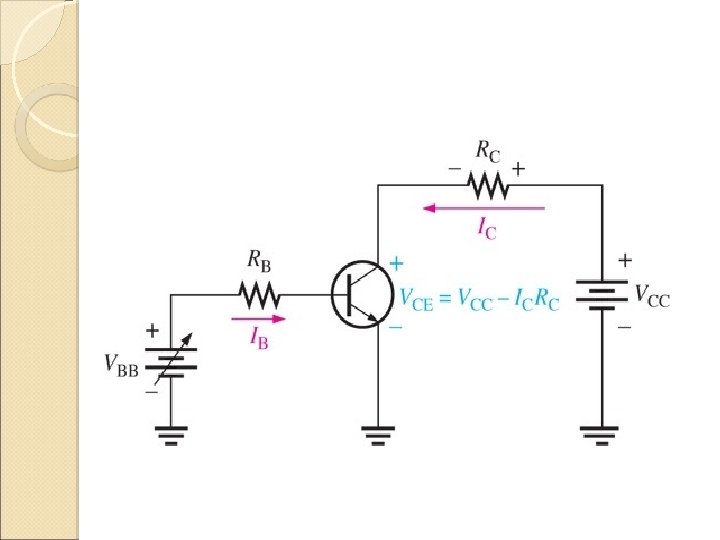
BJT circuit analysis
,")
VBE=0. 7 V based emitter junction is forward biased Since emitter=0 V (ground), by KVL ◦ VRB=VBB-VBE By Ohm’s Law, ◦ VRB=IBRB

Substituting for VRB yields ◦ IBRB=VBB-VBE Solving for IB ◦ IB=VBB-VBE RB

The voltage collector with respect to ground emitter is ◦ VCE=Vcc-VRc Since drop across Rc is ◦ VRC=Ic. Rc Voltage collector with respect to emitter is ◦ Vc. E=Vcc-Ic. Rc

Voltage across reversed-biased collector-base junction ◦ Vc. B=Vc. E-VBE

Collector Characteristics Current
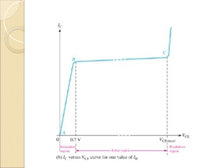
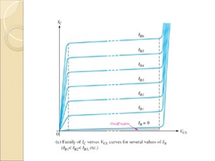

Collector Characteristics Current Shows how collector current Ic varies with collector to emitter voltage VCE for specified value of based IB Vcc=0 Based emitter junction and based collector junction are forward biased VBE=0. 7 V

Assume ◦ VBB produce a certain value of IB ◦ Vcc=0 For this condition, ◦ Base-emitter junction and base-collector junction are forward biased. ◦ Ic=0 ◦ Transistor is in saturation region Saturation ◦ Ic has reached maximum and is independent of IB

As Vcc is increased ◦ Vc. E increases as Ic increases Point A and B

When VCE>0. 7 V, base collector junction becomes reversed biased ◦ Transistor goes into active/linear region ◦ Ic levels constant as VCE continues to increase ◦ Ic increases very slightly as VCE increases due to widening of base-collector depletion region ◦ Fewer holes for recombination in based region Slight increase in ßDC ◦ Point B and C

VCE at sufficiently high voltage, reversed biased base collector junction goes into breakdown ◦ Ic increase rapidly ◦ Point C

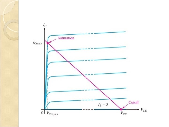
Cutoff Occur when IB=0 Very small amount of collector leakage current, ICEO ◦ Thermally produced carriers ICEO is extremely small and neglected ◦ VCE=Vcc neither base-emitter nor basecollector junction are forward biased
 is extremely small and is usually neglected.")
Cutoff: Collector leakage current (ICEO) is extremely small and is usually neglected.

Saturation When base-emitter junction is forward biased, IB and Ic increase VCE decreases (VCE=Vcc-Ic. Rc) VCE reaches saturation value, VCE(sat), base collector junction becomes forward biased Ic can increase no further Occurs below knee of collector curves

DC Load Line Connecting cutoff point and saturation point Ideal cutoff ◦ Ic=0 ◦ VCE=Vcc Saturation ◦ Ic=Ic(sat) ◦ VCE=VCE(sat)
=0. 2 V")
Determine whether or not transistor is in saturation. Assume VCE(sat)=0. 2 V

Maximum Transistor Rating BJT has limitation on its operation Product of VCE and Ic must not exceed max power dissipation Ic= PD(max) VCE VCE max IC max

Maximum power dissipation curve and tabulated values.

Transistor as an Amplifier ac input voltage produces ac base current large collector current Ac collector current produces dc voltage across Rc thus produces amplified, inverted ac voltage
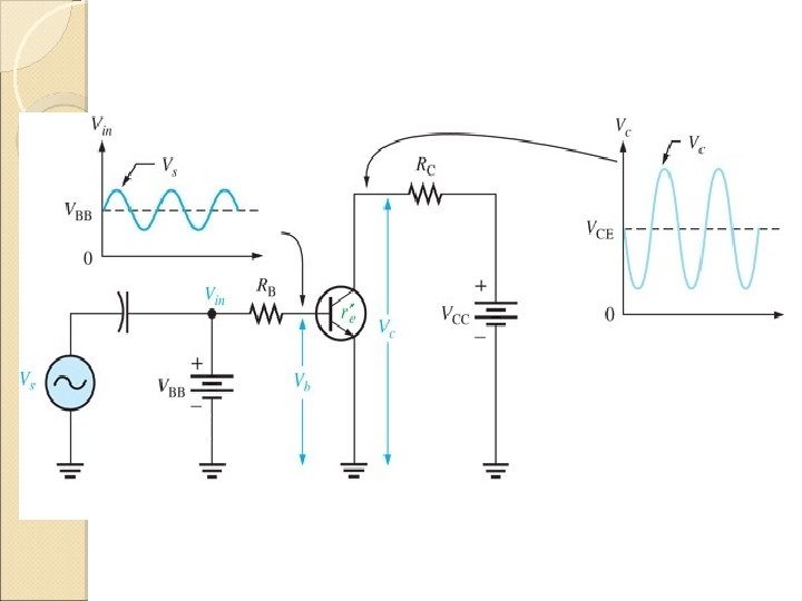

Av=Vc/Vb = I e. R c Ier’e Av=Rc/r’e
")
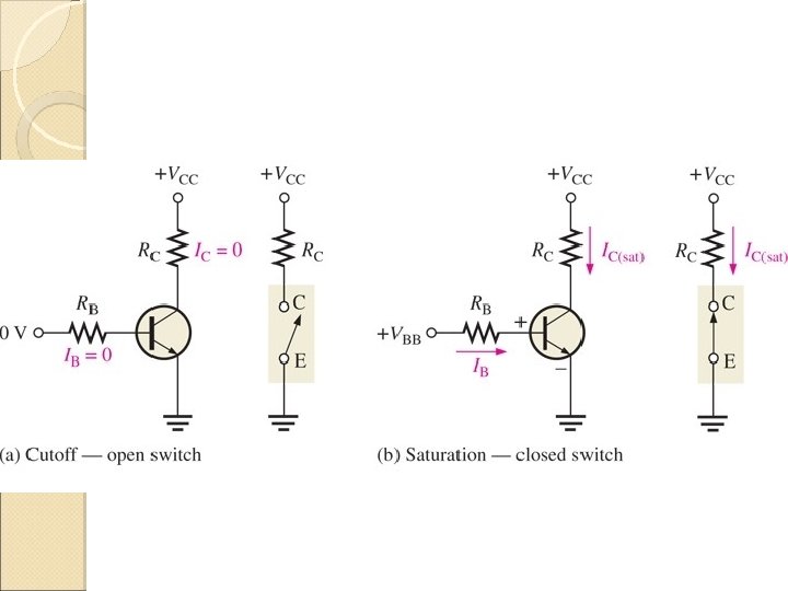
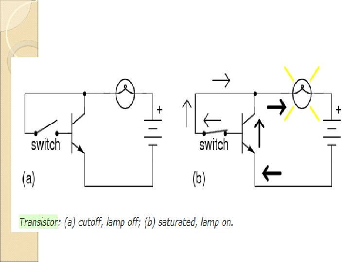
Resistor as a Switch Transistor in cutoff region (base emitter is not forward biased) Open between collector and emitter Neglecting leakage current, all current are zero ◦ Vc. E(cutoff)=Vcc

Transistor in saturation region ◦ Base emitter and base collector junction are forward biased Ib large, Ic reach saturation Short between collector and emitter
=Vcc-Vc. E(sat) Rc Vc. E<<Vcc ◦ Vcc neglected ◦ IB (min) = Ic(sat)")
Ic(sat)=Vcc-Vc. E(sat) Rc Vc. E<<Vcc ◦ Vcc neglected ◦ IB (min) = Ic(sat) ßDC
- Slides: 42