Bioinspired design nonlinear digital pixels for multipletier processes
Bio-inspired design: nonlinear digital pixels for multiple-tier processes (invited paper) SPIE Nano/Bio/Info-Tech Sensors and Systems March 2013 O. Skorka, A. Mahmoodi, J. Li, and D. Joseph Electrical and Computer Engineering University of Alberta, Edmonton, AB, Canada
Outline • Introduction • Bio-inspired design • Nonlinear response • Digital pixels • Multiple-tier processes • Conclusion 2
Introduction • Carver Mead, who cofounded Foveon in 1997, was a pioneer for bio-inspired electronics in the 1980 s. • His work on the “silicon retina” continues to inspire researchers in the image sensor community. • Yet, a design inspired by biological systems too literally does not guarantee comparable functionality. • The approach presented here is more concerned with bio-inspired performance than structure or form. • We use the human eye’s capabilities as benchmarks to motivate and direct research on image sensors, while leveraging existing and emerging technologies. 3
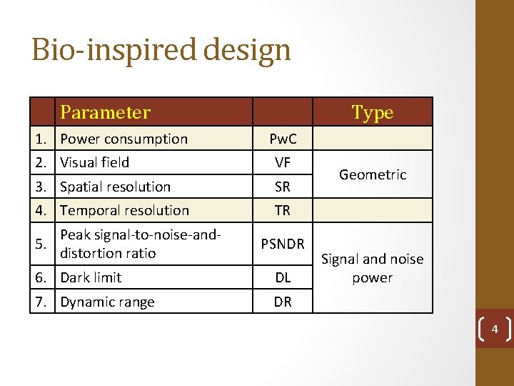
Bio-inspired design Parameter 1. Power consumption Type Pw. C 2. Visual field VF 3. Spatial resolution SR 4. Temporal resolution TR Peak signal-to-noise-and 5. distortion ratio PSNDR 6. Dark limit DL 7. Dynamic range DR Geometric Signal and noise power 4
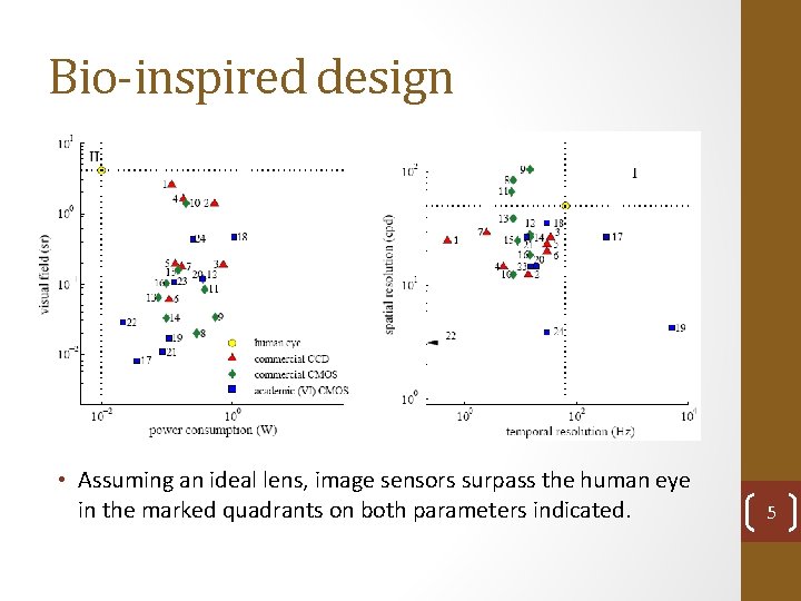
Bio-inspired design • Assuming an ideal lens, image sensors surpass the human eye in the marked quadrants on both parameters indicated. 5
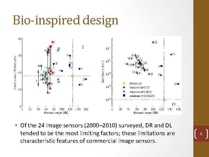
Bio-inspired design • Of the 24 image sensors (2000– 2010) surveyed, DR and DL tended to be the most limiting factors; these limitations are characteristic features of commercial image sensors. 6
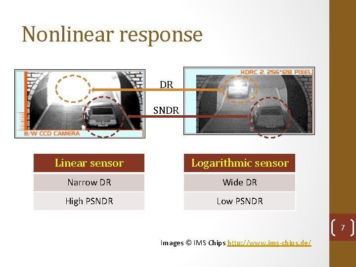
Nonlinear response DR SNDR Linear sensor Logarithmic sensor Narrow DR Wide DR High PSNDR Low PSNDR 7 Images © IMS Chips http: //www. ims-chips. de/
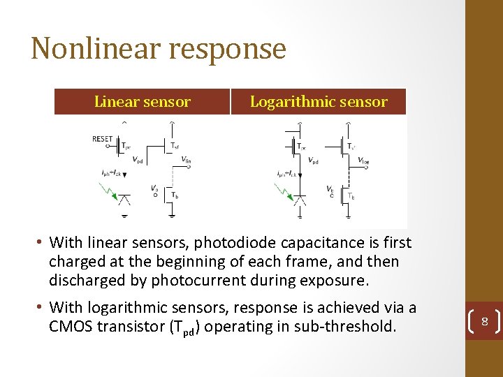
Nonlinear response Linear sensor Logarithmic sensor • With linear sensors, photodiode capacitance is first charged at the beginning of each frame, and then discharged by photocurrent during exposure. • With logarithmic sensors, response is achieved via a CMOS transistor (Tpd) operating in sub-threshold. 8
Nonlinear response • Two paths to achieve wide DR and high PSNDR: • Improve DR of high-PSNDR linear sensors; • Improve SNDR of wide-DR nonlinear sensors. • SNDR is affected by two types of noise: • Temporal noise, i. e. , time-varying noise; • Spatial distortion, i. e. , fixed pattern noise (FPN). • Our team developed new methods for FPN correction, of nonlinear sensors, to the limit of temporal noise. • The methods, which are computationally efficient, are suitable for both still-image and video applications. 9
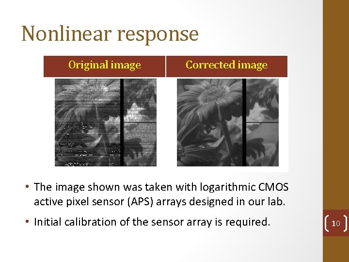
Nonlinear response Original image Corrected image • The image shown was taken with logarithmic CMOS active pixel sensor (APS) arrays designed in our lab. • Initial calibration of the sensor array is required. 10
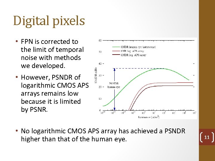
Digital pixels • FPN is corrected to the limit of temporal noise with methods we developed. • However, PSNDR of logarithmic CMOS APS arrays remains low because it is limited by PSNR. • No logarithmic CMOS APS array has achieved a PSNDR higher than that of the human eye. 11
Digital pixels • Linear CMOS APS arrays are integrating designs: • Finite-duration integration approximates a first-order low-pass filter (LPF) with a narrow bandwidth (BW); • The LPF reduces temporal noise, resulting in high PSNR, which enables high PSNDR and high image quality. • Logarithmic CMOS APS arrays are non-integrating: • Consequently, each pixel sensor has a wide BW; • The wide noise spectrum results in low PSNDR. • With CMOS APS arrays, data conversion is done at chip or column level; pixel-level digitization enables noise filtering and protection from further noise. 12
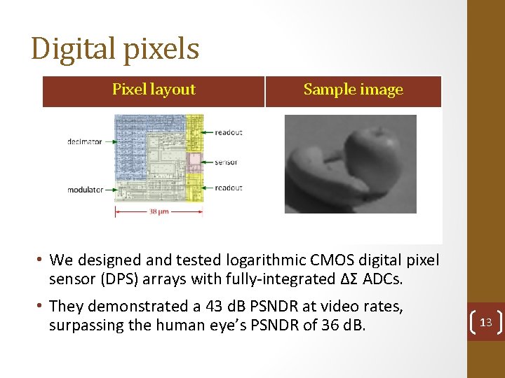
Digital pixels Pixel layout Sample image • We designed and tested logarithmic CMOS digital pixel sensor (DPS) arrays with fully-integrated ΔΣ ADCs. • They demonstrated a 43 d. B PSNDR at video rates, surpassing the human eye’s PSNDR of 36 d. B. 13
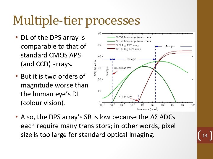
Multiple-tier processes • DL of the DPS array is comparable to that of standard CMOS APS (and CCD) arrays. • But it is two orders of magnitude worse than the human eye’s DL (colour vision). • Also, the DPS array’s SR is low because the ΔΣ ADCs each require many transistors; in other words, pixel size is too large for standard optical imaging. 14
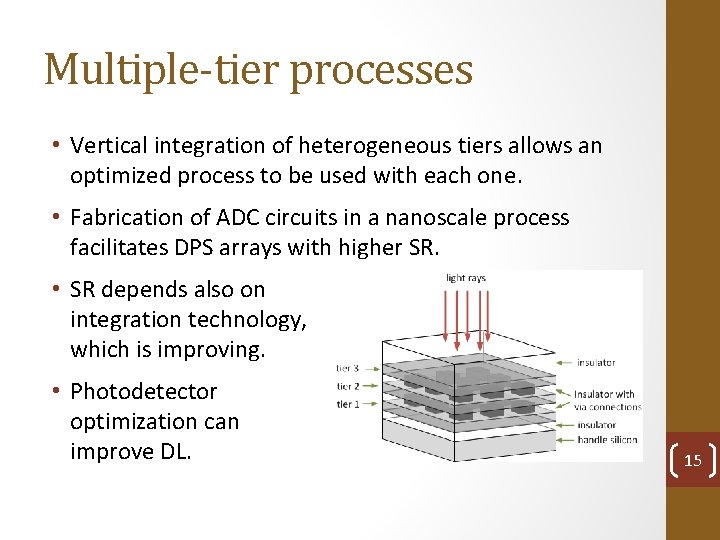
Multiple-tier processes • Vertical integration of heterogeneous tiers allows an optimized process to be used with each one. • Fabrication of ADC circuits in a nanoscale process facilitates DPS arrays with higher SR. • SR depends also on integration technology, which is improving. • Photodetector optimization can improve DL. 15
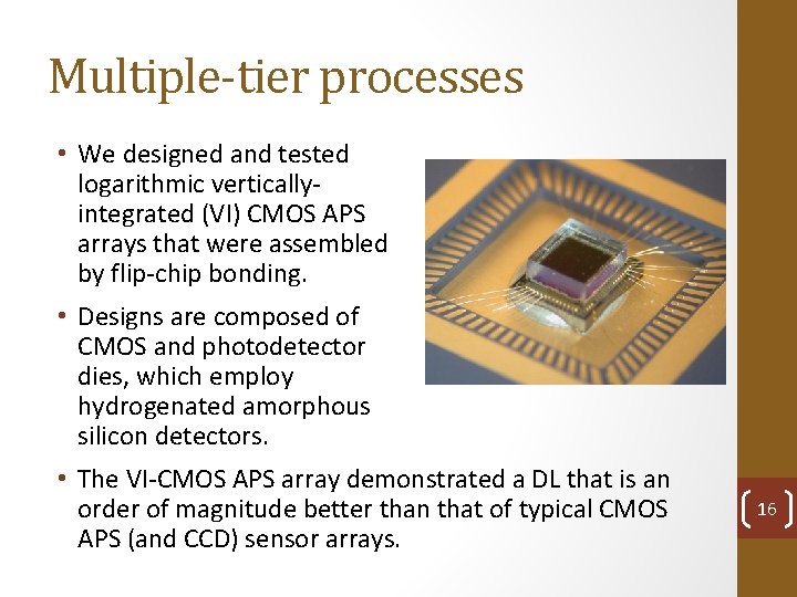
Multiple-tier processes • We designed and tested logarithmic verticallyintegrated (VI) CMOS APS arrays that were assembled by flip-chip bonding. • Designs are composed of CMOS and photodetector dies, which employ hydrogenated amorphous silicon detectors. • The VI-CMOS APS array demonstrated a DL that is an order of magnitude better than that of typical CMOS APS (and CCD) sensor arrays. 16
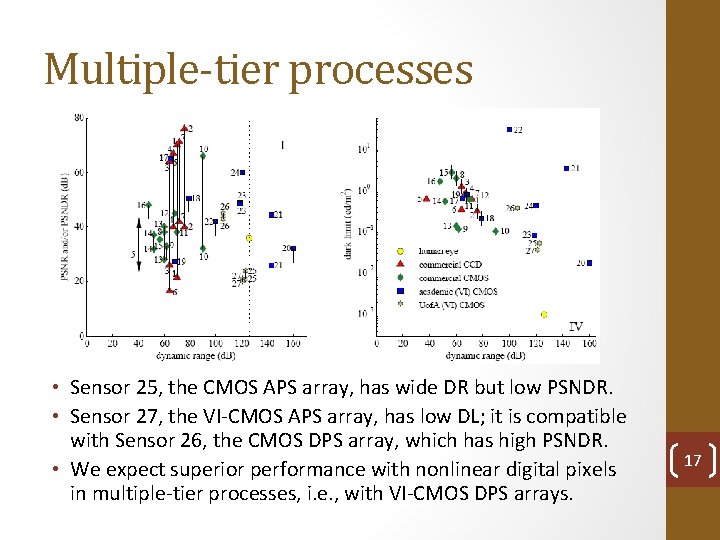
Multiple-tier processes • Sensor 25, the CMOS APS array, has wide DR but low PSNDR. • Sensor 27, the VI-CMOS APS array, has low DL; it is compatible with Sensor 26, the CMOS DPS array, which has high PSNDR. • We expect superior performance with nonlinear digital pixels in multiple-tier processes, i. e. , with VI-CMOS DPS arrays. 17
Conclusion • The approach presented here for image sensor design is inspired by the performance of the corresponding biological system rather than by its structure. • Compared to the human eye, DR and DL are the most limiting factors of conventional image sensors. • FPN of logarithmic CMOS APS arrays, which easily achieve wide DR, can be corrected effectively. • With CMOS DPS arrays, in-pixel ΔΣ ADCs are used to filter temporal noise and achieve high PSNDR. • To achieve low DL, and to pursue high SR, multiple-tier processes, or VI-CMOS technology, is investigated. 18
Acknowledgments • The authors would like to thank: • Dr. Kamal Ranaweera; • Dr. Jianzeng Xu; • Dr. Glen Fitzpatrick; • NSERC; • Alberta Innovates— Technology Futures; • CMC Microsystems; • Micralyne. 19
- Slides: 19