Bias circuit Single stage OTA fully differential opamp
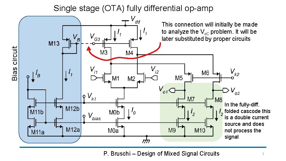
Bias circuit Single stage (OTA) fully differential op-amp M 13 This connection will initially be made to analyze the Vo. C problem. It will be later substituted by proper circuits In the fully-diff. folded cascode this is a double current source and does not process the signal P. Bruschi – Design of Mixed Signal Circuits 1
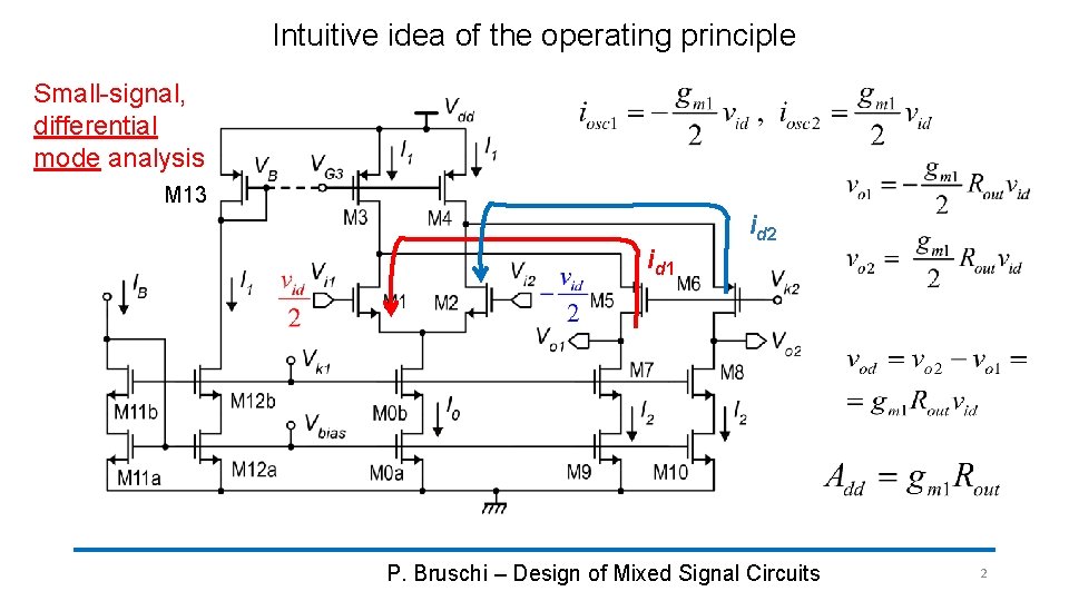
Intuitive idea of the operating principle Small-signal, differential mode analysis M 13 id 2 id 1 P. Bruschi – Design of Mixed Signal Circuits 2
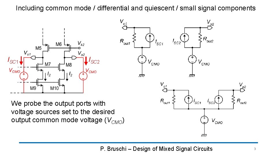
Including common mode / differential and quiescent / small signal components ISC 1 ISC 2 We probe the output ports with voltage sources set to the desired output common mode voltage (VCMO) P. Bruschi – Design of Mixed Signal Circuits 3
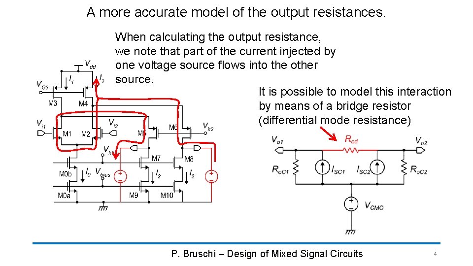
A more accurate model of the output resistances. When calculating the output resistance, we note that part of the current injected by one voltage source flows into the other source. It is possible to model this interaction by means of a bridge resistor (differential mode resistance) P. Bruschi – Design of Mixed Signal Circuits 4
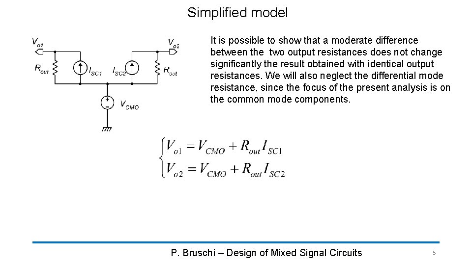
Simplified model It is possible to show that a moderate difference between the two output resistances does not change significantly the result obtained with identical output resistances. We will also neglect the differential mode resistance, since the focus of the present analysis is on the common mode components. P. Bruschi – Design of Mixed Signal Circuits 5
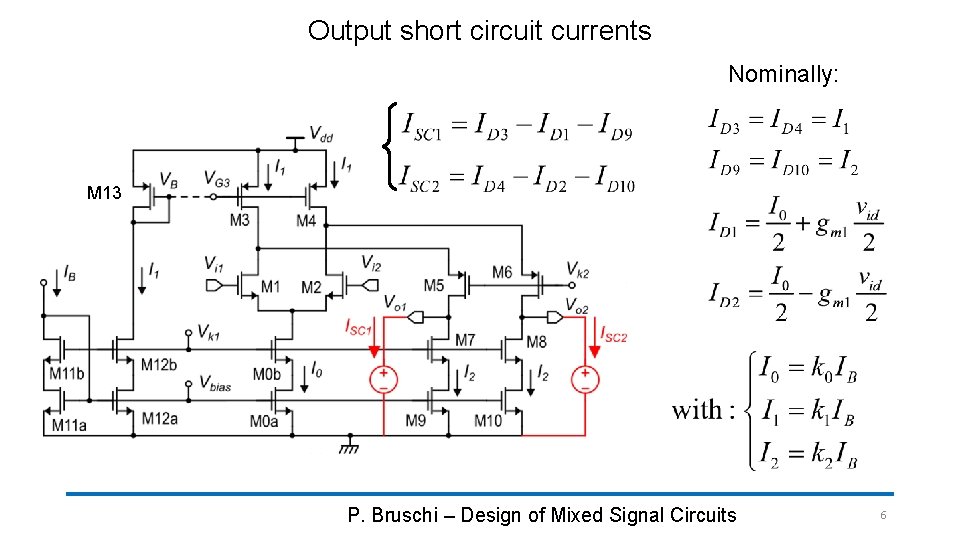
Output short circuit currents Nominally: M 13 P. Bruschi – Design of Mixed Signal Circuits 6
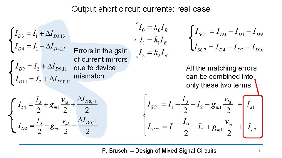
Output short circuit currents: real case Errors in the gain of current mirrors due to device mismatch All the matching errors can be combined into only these two terms P. Bruschi – Design of Mixed Signal Circuits 7
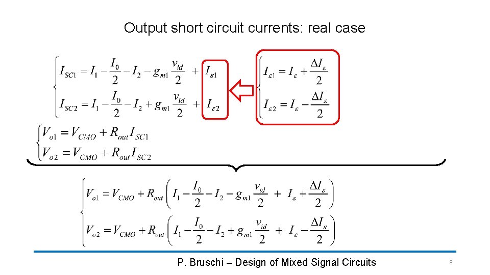
Output short circuit currents: real case P. Bruschi – Design of Mixed Signal Circuits 8
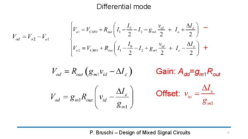
Differential mode + Gain: Add=gm 1 Rout Offset: P. Bruschi – Design of Mixed Signal Circuits 9
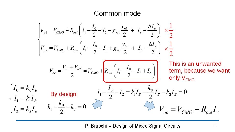
Common mode This is an unwanted term, because we want only VCMO By design: P. Bruschi – Design of Mixed Signal Circuits 10
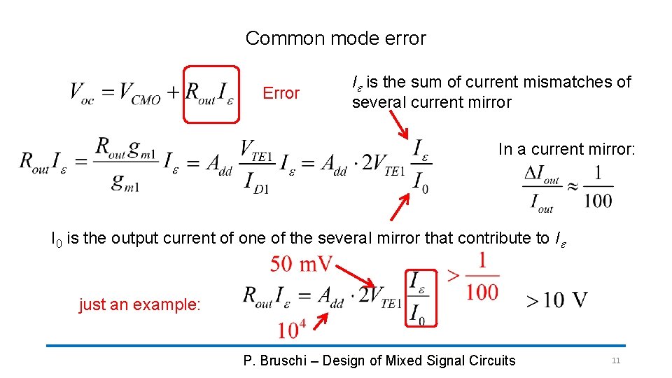
Common mode error Error Ie is the sum of current mismatches of several current mirror In a current mirror: I 0 is the output current of one of the several mirror that contribute to Ie just an example: P. Bruschi – Design of Mixed Signal Circuits 11
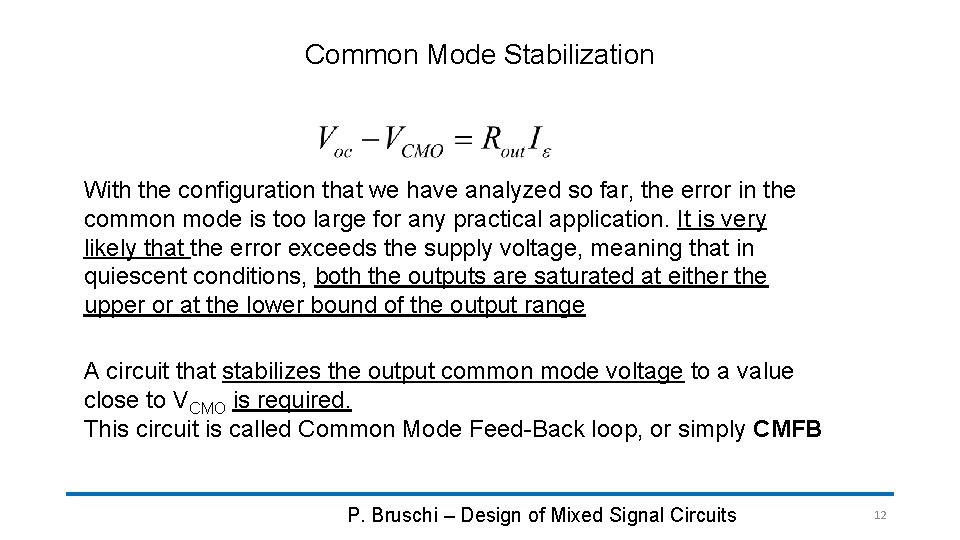
Common Mode Stabilization With the configuration that we have analyzed so far, the error in the common mode is too large for any practical application. It is very likely that the error exceeds the supply voltage, meaning that in quiescent conditions, both the outputs are saturated at either the upper or at the lower bound of the output range A circuit that stabilizes the output common mode voltage to a value close to VCMO is required. This circuit is called Common Mode Feed-Back loop, or simply CMFB P. Bruschi – Design of Mixed Signal Circuits 12
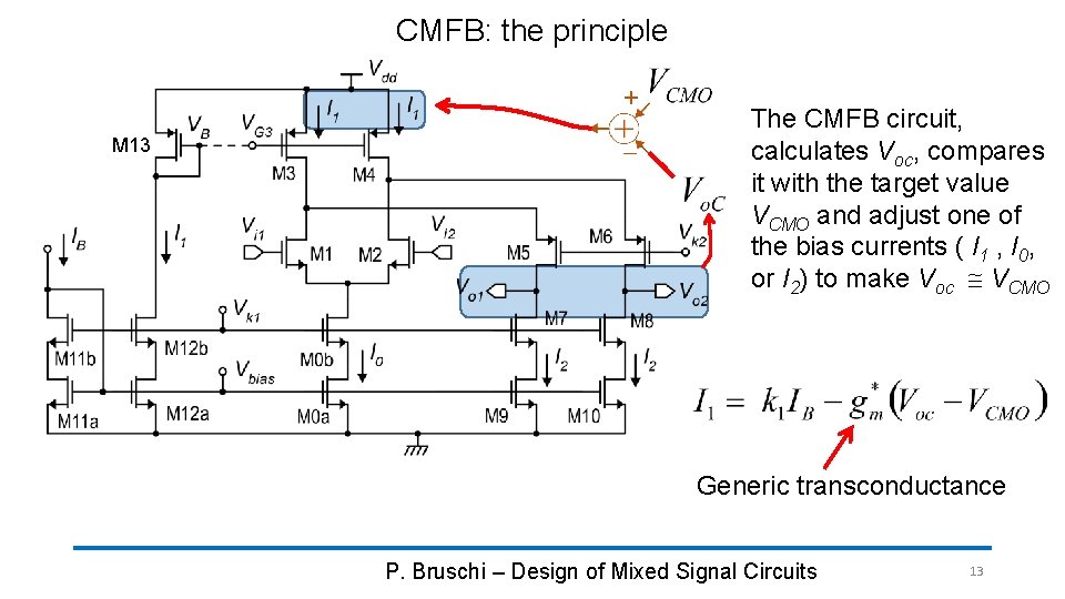
CMFB: the principle M 13 The CMFB circuit, calculates Voc, compares it with the target value VCMO and adjust one of the bias currents ( I 1 , I 0, or I 2) to make Voc VCMO Generic transconductance P. Bruschi – Design of Mixed Signal Circuits 13
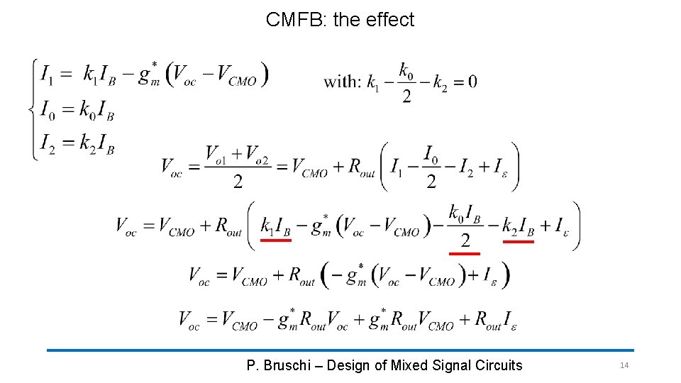
CMFB: the effect P. Bruschi – Design of Mixed Signal Circuits 14
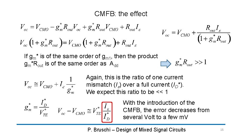
CMFB: the effect If gm* is of the same order of gm 1, then the product gm*Rout is of the same order as Add Again, this is the ratio of one current mismatch (Ie) over a full current (ID*). We expect this ratio to be << 1 With the introduction of the CMFB, the error decreases from several Volt to a few m. V P. Bruschi – Design of Mixed Signal Circuits 15
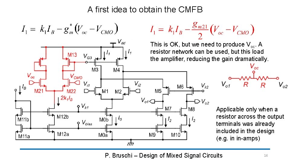
A first idea to obtain the CMFB This is OK, but we need to produce Voc. A resistor network can be used, but this load the amplifier, reducing the gain dramatically. Applicable only when a resistor across the output terminals was already included in the design (e. g. in in-amps) P. Bruschi – Design of Mixed Signal Circuits 16
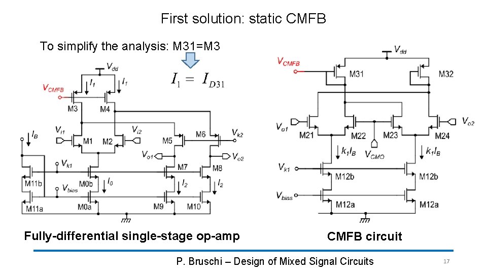
First solution: static CMFB To simplify the analysis: M 31=M 3 Fully-differential single-stage op-amp CMFB circuit P. Bruschi – Design of Mixed Signal Circuits 17
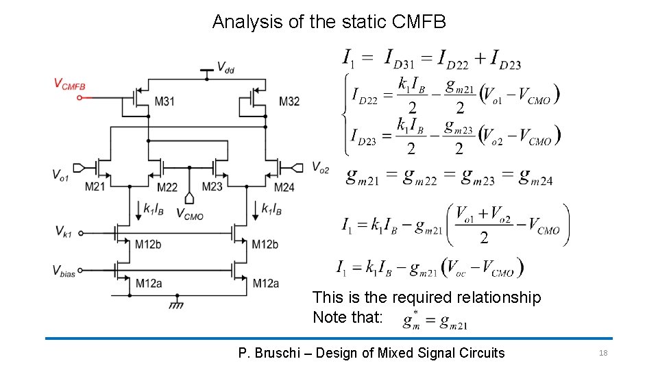
Analysis of the static CMFB This is the required relationship Note that: P. Bruschi – Design of Mixed Signal Circuits 18
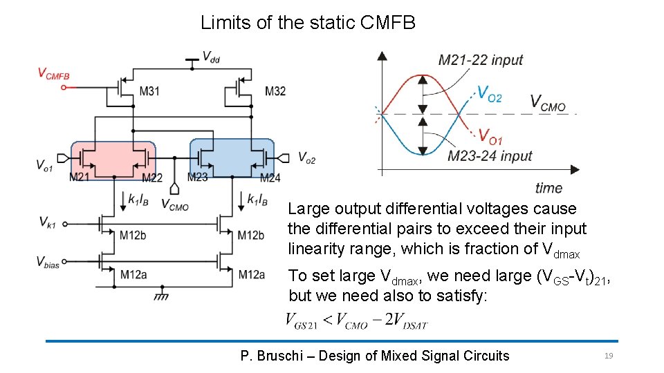
Limits of the static CMFB Large output differential voltages cause the differential pairs to exceed their input linearity range, which is fraction of Vdmax To set large Vdmax, we need large (VGS-Vt)21, but we need also to satisfy: P. Bruschi – Design of Mixed Signal Circuits 19
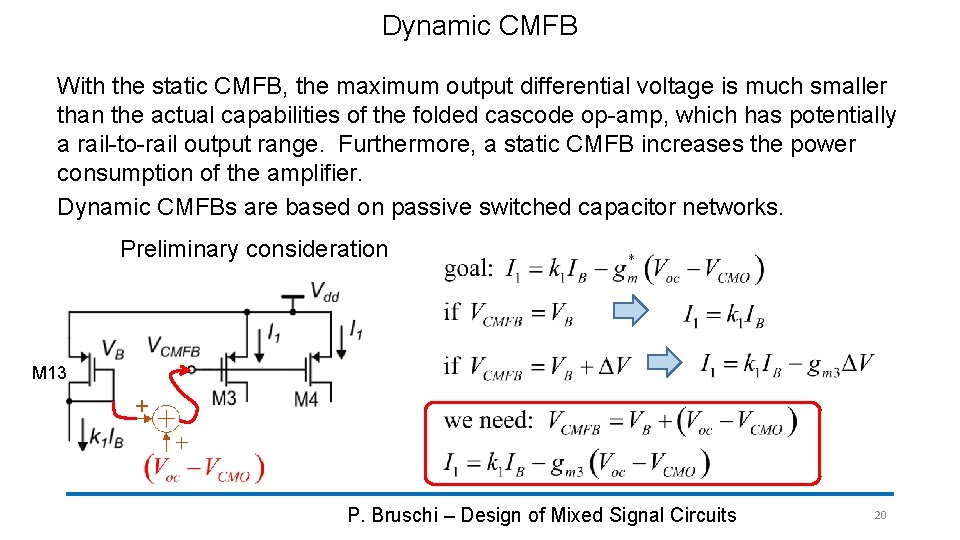
Dynamic CMFB With the static CMFB, the maximum output differential voltage is much smaller than the actual capabilities of the folded cascode op-amp, which has potentially a rail-to-rail output range. Furthermore, a static CMFB increases the power consumption of the amplifier. Dynamic CMFBs are based on passive switched capacitor networks. Preliminary consideration M 13 P. Bruschi – Design of Mixed Signal Circuits 20
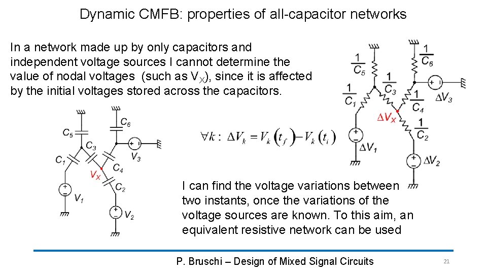
Dynamic CMFB: properties of all-capacitor networks In a network made up by only capacitors and independent voltage sources I cannot determine the value of nodal voltages (such as VX), since it is affected by the initial voltages stored across the capacitors. I can find the voltage variations between two instants, once the variations of the voltage sources are known. To this aim, an equivalent resistive network can be used P. Bruschi – Design of Mixed Signal Circuits 21
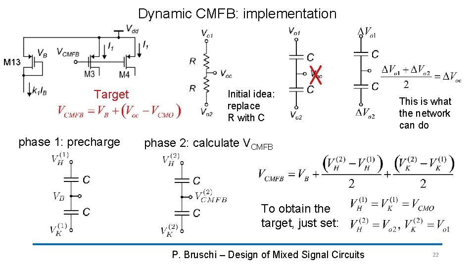
Dynamic CMFB: implementation M 13 Target phase 1: precharge Initial idea: replace R with C This is what the network can do phase 2: calculate VCMFB To obtain the target, just set: P. Bruschi – Design of Mixed Signal Circuits 22
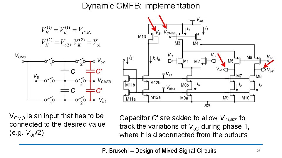
Dynamic CMFB: implementation VCMO is an input that has to be connected to the desired value (e. g. Vdd/2) Capacitor C' are added to allow VCMFB to track the variations of Vo. C during phase 1, where it is disconnected from the outputs P. Bruschi – Design of Mixed Signal Circuits 23
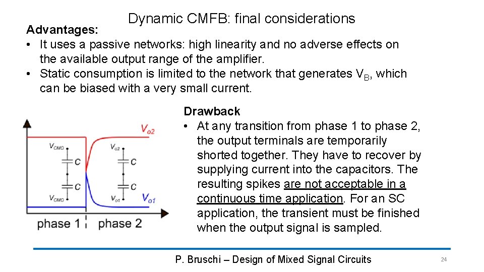
Dynamic CMFB: final considerations Advantages: • It uses a passive networks: high linearity and no adverse effects on the available output range of the amplifier. • Static consumption is limited to the network that generates VB, which can be biased with a very small current. Drawback • At any transition from phase 1 to phase 2, the output terminals are temporarily shorted together. They have to recover by supplying current into the capacitors. The resulting spikes are not acceptable in a continuous time application. For an SC application, the transient must be finished when the output signal is sampled. P. Bruschi – Design of Mixed Signal Circuits 24
- Slides: 24