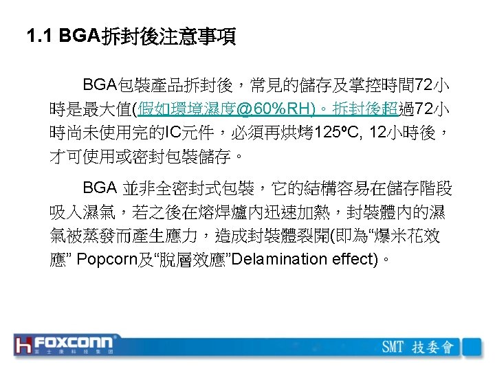
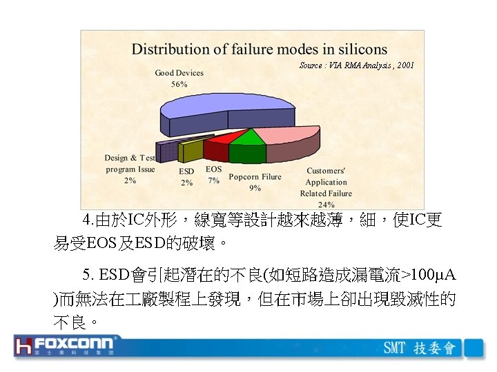
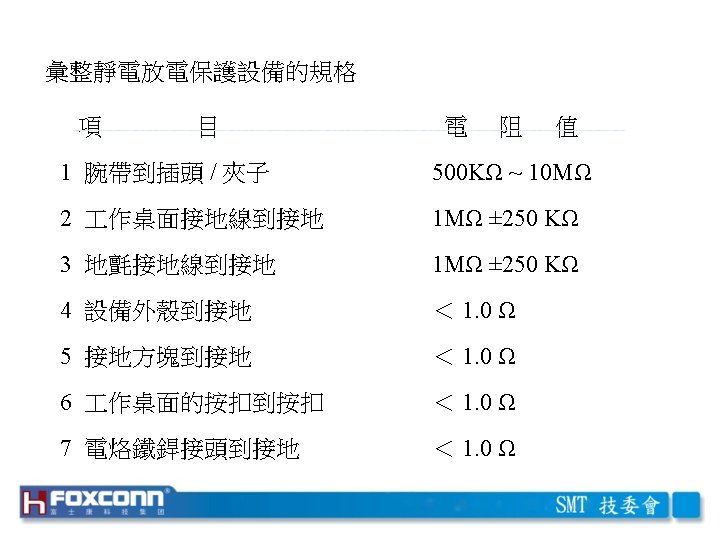
BGA Rework 1 1 BGA 1 2 SAT

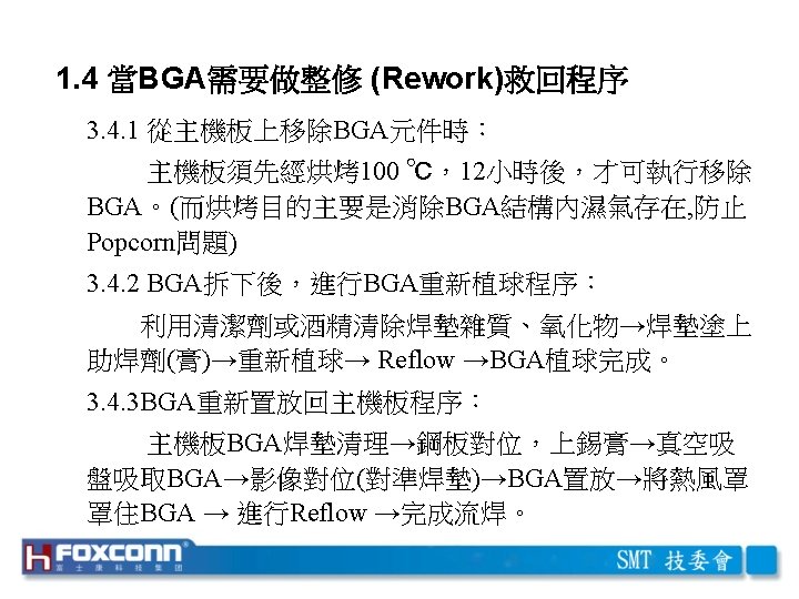
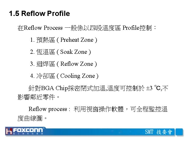
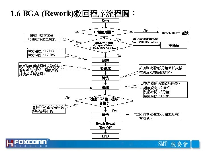
一、BGA Rework 注意事項 1. 1 BGA拆封後注意事項 1. 2 SAT for BGA 1. 3 ummary of transmission X-Ray diagnostic capability 1. 4 當BGA需要做整修 (Rework)救回程序 1. 5 Reflow Profile 1. 6 BGA (Rework)救回程序流程圖 1. 7 VT 8633 Ball-Out Definition
 Normal BGA Devices Chip Die Molding Compound Silver Epoxy Gold Wire Solder Ball")
(1) Normal BGA Devices Chip Die Molding Compound Silver Epoxy Gold Wire Solder Ball Substrate (2) Popcorn or Delam BGA due to Moisture Vaporization during Heating in SMT or Removal (3) Popcorn or Delam BGA due to Plastic Stress Failure Moisture Crack Delamination Void Collapsed Void
 for BGA Normal BGA Devices Delamination or Popcorn")
1. 2 SAT (Scanner Acoustic Tomography) for BGA Normal BGA Devices Delamination or Popcorn BGA Devices, and Red area means Void or Moisture area

1. 3 Summary of transmission X-Ray diagnostic capability Failure Mode Root Cause Ease of Detection Rating 1 ( easy ) … 3… 5 ( hard ) Shorts Opens Shorts Opens Opens Voids Cold Joints Tweaking Debris Excess Paste Popcorning Poor Rework Placement Missing Ball PCB Warp No Paste Dewet Pad Nonwet Bump Reflow/Flux Reflow 1 1 2 1 3 1 1 3 4 5 5 1 1

The Mount-Back Profile of VT 82 C 686 B for VIA BGA Rework Machine ( Vendor : Martin , Model # : MB 1100 )

1. 7 VT 8633 Ball-Out Definition

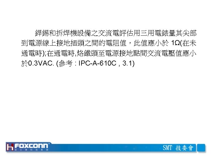
2. 2. 6 EOS 不良品分析圖片: a. EOS 嚴重燒毀之外觀不良 IC 圖片: Serious Burn out area by EOS b. EOS 嚴重燒毀之Chip F. A. 圖片(1): Burn-out spot GND core (Metal 3) of VT 82 C 586 B was burned out VDD-5 VSTB core (Metal 2) of VT 82 C 586 B was serious burned out
 GND and VCC 3. 3 V of")
c. EOS 嚴重燒毀之 Chip F. A. 圖片(2) GND and VCC 3. 3 V of VT 82 C 598 MVP were serious burned out.
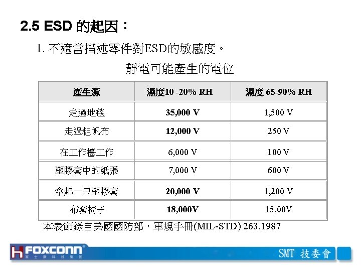

ESD Model Charged Device Model C approx. 3 p. F R approx. 25 ohms (Ω) L approx. 10 n. H Human Body Model C = 100 p. F R = 1500 ohms (Ω) Machine Model C = 200 p. F L = 0. 75 μH (1) The Human Body Model (HBM) is the ESD testing standard, andis defined in the MIL-STD-883 C method 3015. 7. It representsa charged person touching agrounded device. It is the originalmodel used to simulate ESDdamage by a human, and is themost well known. EOS/ESDAssociation Standard S 5. 1 – 1993 describes use of the HBM for device classification.
 The Machine Model (MM) represents a worst case HBM. It provide more realisticsimulation")
(2) The Machine Model (MM) represents a worst case HBM. It provide more realisticsimulation of actual damage normally obtained from a person holding a tool. EOS/ESDAssociation Draft Standard DS 5. 2 – 1993 describes use of the HBM for device classificationand has been released for comment. (3) The Charged Device Model (CDM) simulates the damage resulting from a charged devicecontacting a metal grounded surface. This failure mode is very damaging and is associatedwith automated handling equipment and use of dip tubes. EOS/ESD Association Draft. Standard DS 5. 3 – 1993 describes use of the CDM for device classification and has beenreleased for comment.

5. ESD 不良品分析圖片: SEM photo showing holes at the silicon to field oxide interface in the drain diffusion of an FOD protection device SEM photo of drain/gate diffusion edge damage SEM photo of an n. MOS transistor in an output buffer showing damage at the drain/gate diffusion edge. SEM photo of silicon melting due to current filamentation in a n. MOS output transistor

SEM photo of damage due to a polycrystalline filament in a trick oxide device. SEM photo of a contact hole in the drain diffusion of an output transistor showing contact spiking. a. VT 3091 A ESD_HBM pad 60(Lvref) fail Pad 60 (Lvref) Poly gate The SEM photograph of the contact burn out at ESD protection circuit of pad 60 (Lvref) for. VT 3091 A device
 fail Pad 63 (VCC 2) The")
b. VT 3091 A ESD_HBM pad 63(VCC 2) fail Pad 63 (VCC 2) The OM and SEM photograph of the poly burn out at pad 63 (VCC 2) for VT 3091 A device Poly layer Pad 63 (VCC 2)

6. The analysis flow of return samples is as follows : Receive return samples External Visual Pass to subcontractor Fail Scanning Acoustic Tomography (SAT) Pass Baking 12 hours, 125℃ F/A Re-ball Pass Fail Function test (ATE) Download datalog Test on Bench Board Pass Fail F/A (X-Ray, Decap) Return samples to customer Analyze failure mode F/A report
- Slides: 52