Beyond Si MOSFETs Part IV Alternative Transistor Structures

Beyond Si MOSFETs Part IV
 technology • Multistage transistor")
Alternative Transistor Structures • Silicon-on -insulator (SOI) technology • Multistage transistor

CMOS scaling bottleneck Sub threshold slope § Increase of off-state leakage currents with decreasing threshold voltage § Increase of sub-threshold slope as doping density in channel cannot be increased without paying in mobility Gate leakage § Increase of gate leakage currents due to tunneling effects
 on the")
Double gate FETs Single gating Double gating Increases control of the gate(s) on the channel • 2 nd gate shields drain • 2 nd gate allows DT mode • Higher current drive

Double gate FETs Capacitive coupling Single gating Double gating

Advantages double gating Reduction of DIBL Improved sub-threshold slope S
. • Prophesized to show")
Why Multi-Gate SOI MOSFETs? • Higher current drift (better performance). • Prophesized to show higher tolerance to scaling. • Better integration feasibility, raised source-drain structure, ease in integration. • Larger number of parameters to tailor device performance.

Double Gate FETs Control of VT Via doping of the substrate, however in very small devices in-homogeneity local number/”nano-scopic” volume Undoped substrate, using metal gates - Choice of workfunctions larger than with n or p-doped poly. Si Asymmetric gates - Workfunction of the two gates different: -Top gate: channel inversion -Bottom gate : bulk control - 1 channel Symmetric gates - Workfunction of the two gates same: -Top gate : channel inversion -Bottom gate: channel inversion - 2 channels- possibly interacting

Double gate FETs Energy bands- same voltage on both gates

Double gate FETs Energy bands- different voltages on both gates Cfr. a-symmetric gate Voltage on the 2 nd gate influences the threshold voltage of the first gate. - 2 nd gate controls the value of the threshold voltage. - 2 nd gate can shift VT to required value

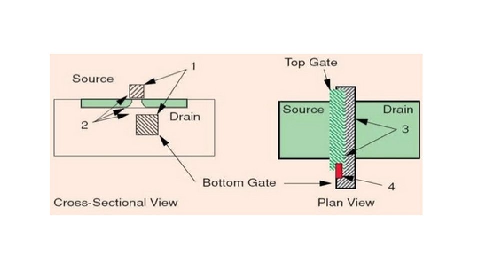
Double gate FETs Gate alignment Problems that have hindered progress of the DGFET approach are: Alignment issues: 1) Definition of both gates to the same image size accurately. 2) Self alignment of the source/drain regions to both top and bottom gates. 3) Alignment of the two gates to one another. 4) Connecting two gates with a low-resistance path. These are needed for high current drive and low capacitances. Circuit design issue: Ø Area efficient means needs to be designed to connect the two gates together.

Layout of Double Gate v Type I : Planar Double Gate v Type II : Vertical Double Gate v Type III : Horizontal Double Gate (Fin. FET)

3 DG-FET Structures Problems: alignments of gates Contacting gates.

3 DG-FET structures

3 DG-FET structures

FET parameters defined by lithography Type S-D direction Gate to gate direction Gate length control (L) Channel thickness control (W) Top area I In plane Perpendicular to plane Litho/etch Planar layer Lx. W II Perpendicular to plane In plane Planar layer Litho/etch Wx. H II In plane Litho/etch Litho etch Lx. H

And the winner is…fin. FETs • No gate alignment problems. • Independent gate control possible. • CMOS compatible processing ‘’trick’’ using side wall spacer technology to define the fin but not straightforward.
 Non-classical FET structures Devices SOI Band engineered")
Solutions for the Short Channel Effect (SCE) Non-classical FET structures Devices SOI Band engineered FET Double gate FET Concept Fully depleted channel on oxide MODFET/strained Si channels Vertical FETs/gate surround or two gates Advantages S, VT control Ion , f. T Ion , S, SCE Scaling issues Si thickness, SCE BC, QW thickness Processing complexity, Si thickness, QM effects
- Slides: 19