Beyond Moores Law Physical limits of silicon MOSFET
Beyond “Moore’s Law”: Physical limits of silicon MOSFET transistors 2017 -04 -05 Julian Nowaczek

MOSFET Scaling: Introduction What do I mean by “scaling”? Decreasing transistor size to: Fit more devices in the same area Decrease power consumption Increase switching speed A majority of the historical gains in performance and power efficiency are a direct result of shrinking FET dimensions Several orders of magnitude smaller dimensions mean that effects that were previously negligible can become highly problematic What sort of effects? What techniques can be used to mitigate these issues?
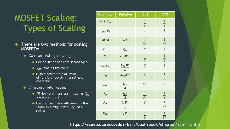
Parameter MOSFET Scaling: Types of Scaling Relation CVS CFS There are two methods for scaling MOSFETs: Constant Voltage scaling Device dimensions are scaled by S VDD remains the same High electric field at small dimensions results in unreliable operation Constant Field scaling All device dimensions including are scaled by S VDD Electric field strength remains the same, avoiding instability (to a point) https: //ecee. colorado. edu/~bart/book/chapter 7/ch 7_7. htm
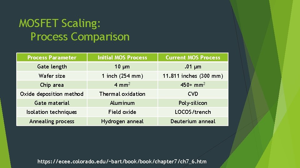
MOSFET Scaling: Process Comparison Process Parameter Initial MOS Process Current MOS Process Gate length 10 μm . 01 μm Wafer size 1 inch (254 mm) 11. 811 inches (300 mm) Chip area 4 mm 2 450+ mm 2 Oxide deposition method Thermal oxidation CVD Gate material Aluminum Poly-silicon Isolation techniques Field oxide LOCOS/trench Annealing process Hydrogen anneal Deuterium anneal https: //ecee. colorado. edu/~bart/book/chapter 7/ch 7_6. htm
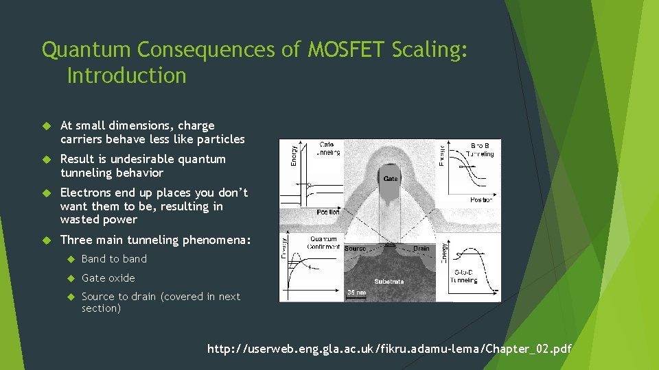
Quantum Consequences of MOSFET Scaling: Introduction At small dimensions, charge carriers behave less like particles Result is undesirable quantum tunneling behavior Electrons end up places you don’t want them to be, resulting in wasted power Three main tunneling phenomena: Band to band Gate oxide Source to drain (covered in next section) http: //userweb. eng. gla. ac. uk/fikru. adamu-lema/Chapter_02. pdf
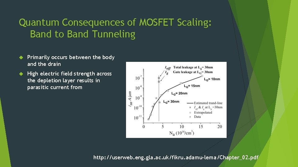
Quantum Consequences of MOSFET Scaling: Band to Band Tunneling Primarily occurs between the body and the drain High electric field strength across the depletion layer results in parasitic current from http: //userweb. eng. gla. ac. uk/fikru. adamu-lema/Chapter_02. pdf
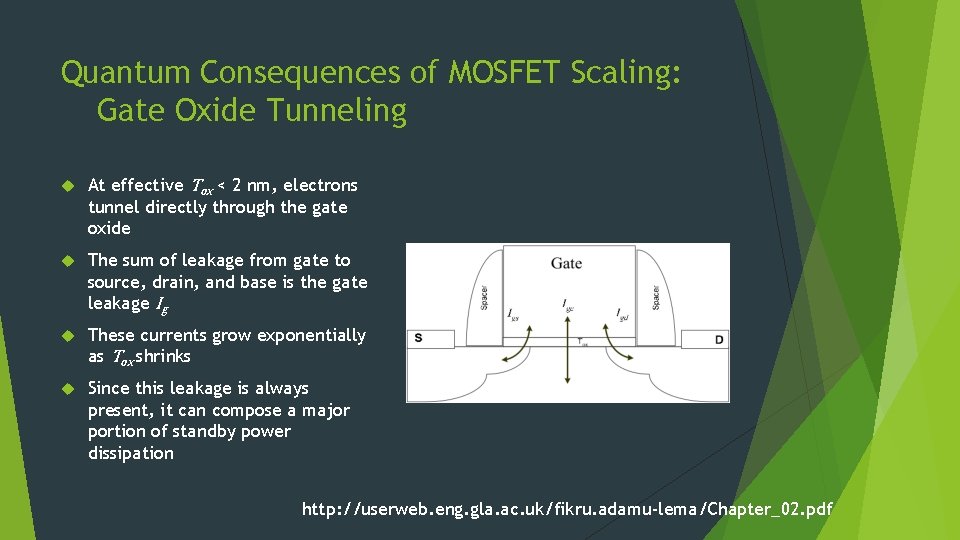
Quantum Consequences of MOSFET Scaling: Gate Oxide Tunneling At effective Tox < 2 nm, electrons tunnel directly through the gate oxide The sum of leakage from gate to source, drain, and base is the gate leakage Ig These currents grow exponentially as Tox shrinks Since this leakage is always present, it can compose a major portion of standby power dissipation http: //userweb. eng. gla. ac. uk/fikru. adamu-lema/Chapter_02. pdf
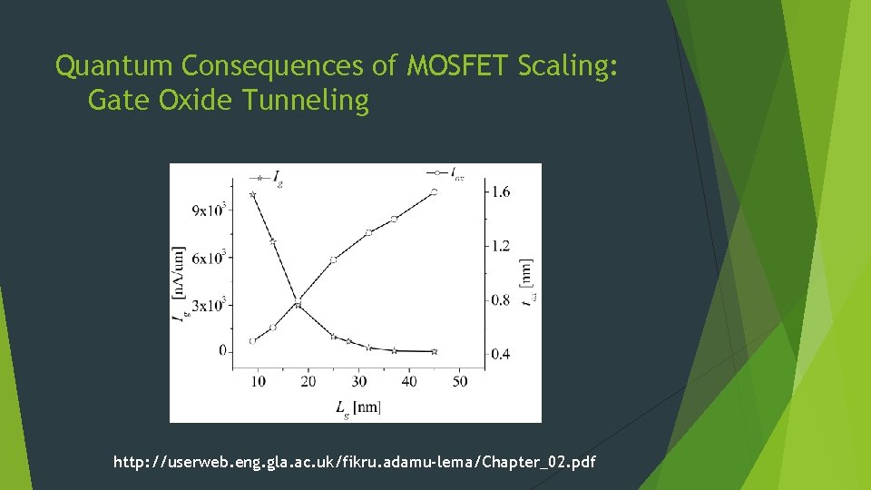
Quantum Consequences of MOSFET Scaling: Gate Oxide Tunneling http: //userweb. eng. gla. ac. uk/fikru. adamu-lema/Chapter_02. pdf

Quantum Consequences of MOSFET Scaling: Source to Drain Tunneling Becomes a limiting factor in transistors with gate length L ≤ 10 nm Source drain tunneling significantly impacts subthreshold operation Difficult to avoid http: //www. crcnetbase. com/doi/pdfplus/10. 1201/9781420028645. ch 3
Short-Channel Effects: Introduction Short-channel effects manifest when gate length is on the same order of magnitude as depletion layer width Five different short-channel effects Drain-induced barrier lowering (DIBL) Surface scattering Velocity saturation Impact ionization Hot carrier injection All arise from stronger magnetic fields Even when designing with constant field in mind, VDS can only scale so far because of power supply concerns
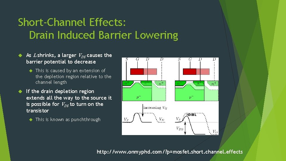
Short-Channel Effects: Drain Induced Barrier Lowering As L shrinks, a larger VDS causes the barrier potential to decrease This is caused by an extension of the depletion region relative to the channel length If the drain depletion region extends all the way to the source it is possible for VDS to turn on the transistor This is known as punchthrough http: //www. onmyphd. com/? p=mosfet. short. channel. effects
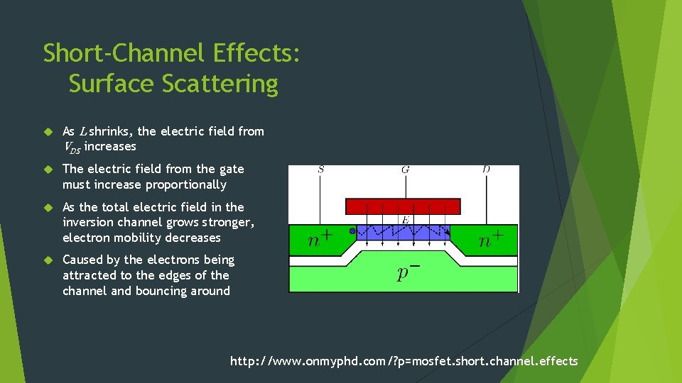
Short-Channel Effects: Surface Scattering As L shrinks, the electric field from VDS increases The electric field from the gate must increase proportionally As the total electric field in the inversion channel grows stronger, electron mobility decreases Caused by the electrons being attracted to the edges of the channel and bouncing around http: //www. onmyphd. com/? p=mosfet. short. channel. effects
Short-Channel Effects: Velocity Saturation Charge carrier velocity is proportional to electric field strength for small electric fields In silicon carrier velocity peaks at around 107 cm/s In short-channel MOSFETs the electric field can surpass the critical point where carrier velocity saturates This results in a lower than expected ID
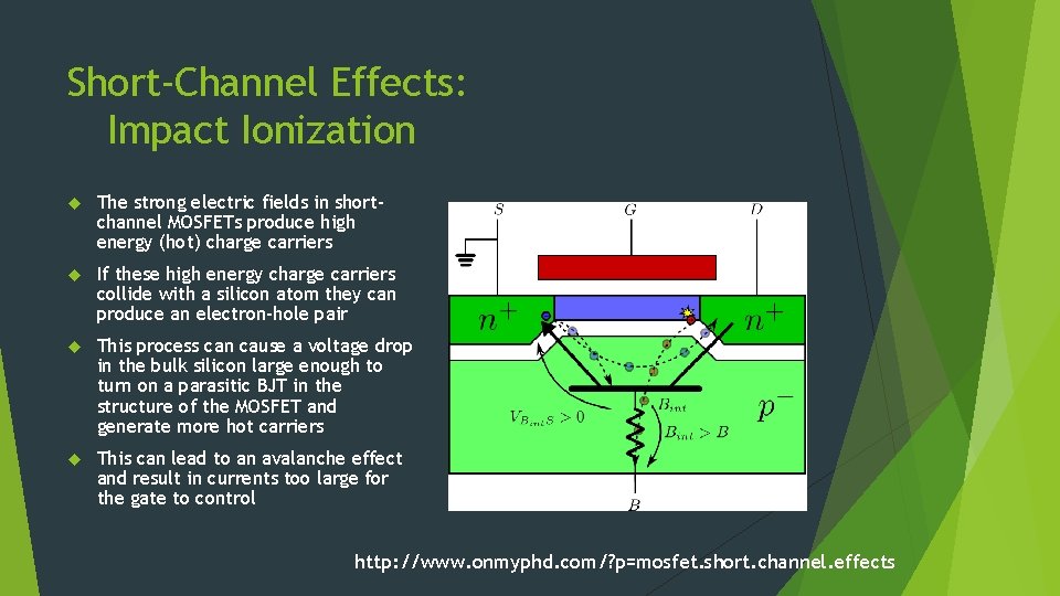
Short-Channel Effects: Impact Ionization The strong electric fields in shortchannel MOSFETs produce high energy (hot) charge carriers If these high energy charge carriers collide with a silicon atom they can produce an electron-hole pair This process can cause a voltage drop in the bulk silicon large enough to turn on a parasitic BJT in the structure of the MOSFET and generate more hot carriers This can lead to an avalanche effect and result in currents too large for the gate to control http: //www. onmyphd. com/? p=mosfet. short. channel. effects
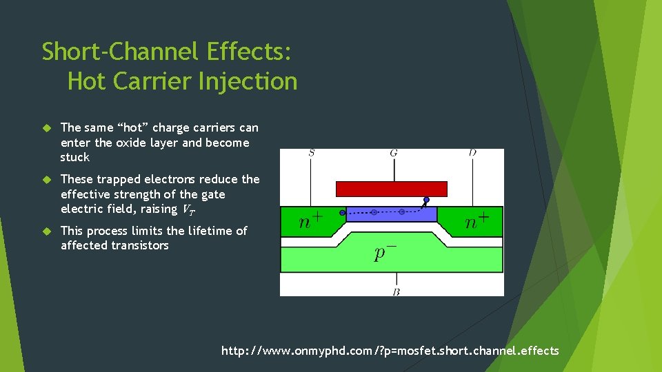
Short-Channel Effects: Hot Carrier Injection The same “hot” charge carriers can enter the oxide layer and become stuck These trapped electrons reduce the effective strength of the gate electric field, raising VT This process limits the lifetime of affected transistors http: //www. onmyphd. com/? p=mosfet. short. channel. effects
Other Issues Heat dissipation What happens when MOSFETs get too hot? Hint: They heat up more Gate oxide reliability Intrinsic parameter fluctuations Is Si. O 2 a good enough insulator? What happens when structures are so small that the random distribution of dopant atoms isn’t uniform enough? Speed of light How big can my chip get? How fast can I get data in and out?

Potential Solutions: Introduction That all sounds bad It is, but… There are solutions to many of these problems Different materials and structures hold significant promise Silicon on insulator High-κ Metal Gate (HKMG) Alternative gate geometries (multigate devices) Subthreshold operation Optical interconnects A few of these techniques are already in devices you use every day Research is ongoing for new techniques and materials to supplement these as there is still demand for better power efficiency and performance
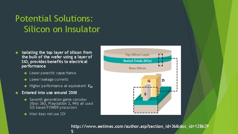
Potential Solutions: Silicon on Insulator Isolating the top layer of silicon from the bulk of the wafer using a layer of Si. O 2 provides benefits to electrical performance Lower parasitic capacitance Lower leakage currents Higher performance at equivalent VDS Entered into use around 2000 Seventh generation game consoles (Xbox 360, Playstation 3, Wii) all used SOI based POWER processors Intel does not use SOI http: //www. eetimes. com/author. asp? section_id=36&doc_id=128629 5
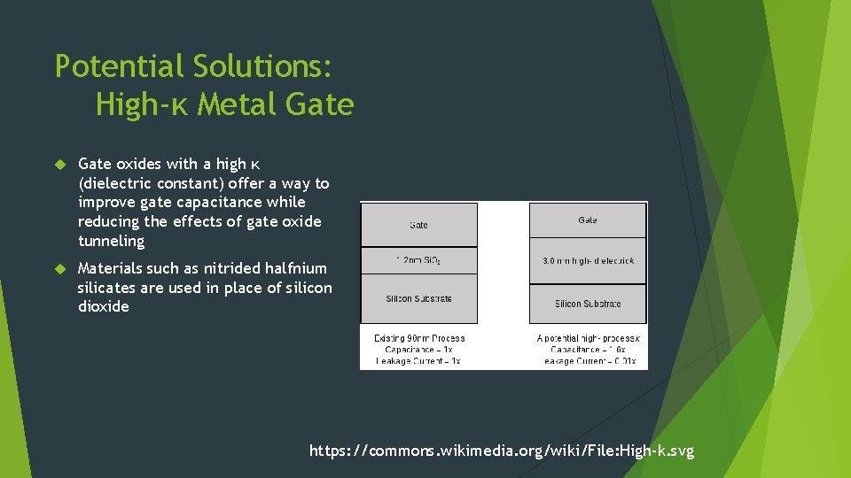
Potential Solutions: High-κ Metal Gate oxides with a high κ (dielectric constant) offer a way to improve gate capacitance while reducing the effects of gate oxide tunneling Materials such as nitrided halfnium silicates are used in place of silicon dioxide https: //commons. wikimedia. org/wiki/File: High-k. svg

Potential Solutions: Mulitigate Devices Multigate MOSFETs offer better electrostatic integrity than planar MOSFETs and therefore allow for lower VDS Fin. FETs likely already power some of the computing devices you own Intel began using Fin. FETs in fourthgeneration Core (Haswell) microprocessors i. Phone SOCs A 9 (i. Phone 6 S) or newer Most Samsung Exynos 7 (Galaxy S 6) or newer https: //commons. wikimedia. org/wiki/File: Multigate_models. png
Solutions: Subthreshold Operation Subthreshold operation refers to MOSFET circuits that operate below VT, where the transistor would not normally be considered “on” By operating in this region, the transistor draws only a tiny fraction of the power compared to normal MOSFET regions of operation An example application of this is a wearable sensor powered by body heat. While this would not provide enough power for a conventional microprocessor, subthreshold logic would operate just fine
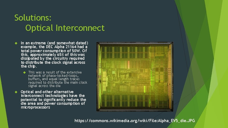
Solutions: Optical Interconnect In an extreme (and somewhat dated) example, the DEC Alpha 21164 had a total power consumption of 50 W. Of this, approximately 65% of this was dissipated by the circuitry required to distribute the clock signal across the chip. This was a result of the extensive network of phase-locked-loops, buffers, and equal length traces required to distribute the main clock signal across the die Optical and other alternative interconnect technologies have the potential to significantly reduce the die area and power consumption of microprocessors https: //commons. wikimedia. org/wiki/File: Alpha_EV 5_die. JPG

References http: //userweb. eng. gla. ac. uk/fikru. adamu-lema/Chapter_02. pdf http: //inst. eecs. berkeley. edu/~ee 130/sp 06/chp 7 full. pdf http: //courses. ece. ubc. ca/579. lect 6. leakagepower. 08. pdf https: //ecee. colorado. edu/~bart/book/chapter 7/ch 7_7. htm https: //ece. uwaterloo. ca/~msachdev/ECE 637/OH_MOS. pdf http: //www. onmyphd. com/? p=mosfet. short. channel. effects http: //www. crcnetbase. com/doi/pdfplus/10. 1201/9781420028645. ch 3 http: //www. eng. auburn. edu/~agrawvd/THESIS/CHANDRAN/MEEProj_Chandran_20 13. pdf http: //www. eetimes. com/author. asp? section_id=36&doc_id=1286295 https: //mat. exon. name/eehons/thesis-html/node 19. html https: //people. eecs. berkeley. edu/~tking/presentations/King. Liu_SOI 2012
Final Exam Concepts Because VDS does not scale as well as the physical dimensions of the MOSFET, the strengthening electric field produced by the source-drain current is a significant problem. That strong electric field causes the electrons in the inversion channel to behave badly, worsening performance or even destroying the device. As the gate length decreases, quantum mechanical effects manifest and lead to increased current leakage through tunneling. Operating a MOSFET below VT is possible and actually useful! All of the computing devices you use daily incorporate technologies beyond the basic bulk MOSFET in order to deliver the performance and efficiency we demand of them.
- Slides: 24