Benchmarking EUV Mask Inspection Beyond 0 25 NA

Benchmarking EUV Mask Inspection Beyond 0. 25 NA The SEMATECH Berkeley Actinic Inspection Tool A I T An EUV-wavelength mask inspection microscope Advanced Materials Research Center, AMRC, International SEMATECH Manufacturing Initiative, and ISMI are servicemarks of SEMATECH, Inc. SEMATECH, the SEMATECH logo, Advanced Technology KAGoldberg @ lbl. gov Development Facility, ATDF, and the ATDF logo are registered servicemarks of SEMATECH, Inc. All other servicemarks and trademarks are the property of their respective owners. SEMATECH Berkeley Actinic Inspection Tool SPIE Photomask BACUS 2008 1
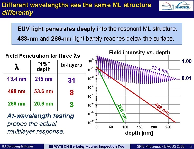
Different wavelengths see the same ML structure differently EUV light penetrates deeply into the resonant ML structure. 488 -nm and 266 -nm light barely reaches below the surface. Field Penetration for three s "1%" depth bi-layers 13. 4 nm 215 nm 31 488 nm 53. 6 nm 8 266 nm 20. 6 nm 3 At-wavelength testing probes the actual multilayer response. KAGoldberg @ lbl. gov Field intensity vs. depth 1. 00 0. 01 depth [nm] SEMATECH Berkeley Actinic Inspection Tool SPIE Photomask BACUS 2008 2

Benchmarking EUV Mask Inspection Beyond 0. 25 NA LBNL: Kenneth A. Goldberg, Iacopo Mochi, Patrick Naulleau AMD: Bruno La. Fontaine Samsung: Hakseung Han SEMATECH: Sungmin Huh Upgrades Resolution (Uniformity) Aberrations Modeling, Measurement, Reduction Linewidth Measurement, Repeatability Advanced Materials Research Center, AMRC, International SEMATECH Manufacturing Initiative, and ISMI are servicemarks of SEMATECH, Inc. SEMATECH, the SEMATECH logo, Advanced Technology KAGoldberg @ lbl. gov Development Facility, ATDF, and the ATDF logo are registered servicemarks of SEMATECH, Inc. All other servicemarks and trademarks are the property of their respective owners. SEMATECH Berkeley Actinic Inspection Tool SPIE Photomask BACUS 2008 3
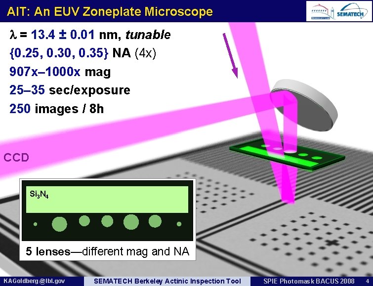
AIT: An EUV Zoneplate Microscope = 13. 4 ± 0. 01 nm, tunable {0. 25, 0. 30, 0. 35} NA (4 x) 907 x– 1000 x mag 25– 35 sec/exposure 250 images / 8 h CCD Si 3 N 4 5 lenses—different mag and NA KAGoldberg @ lbl. gov SEMATECH Berkeley Actinic Inspection Tool SPIE Photomask BACUS 2008 4
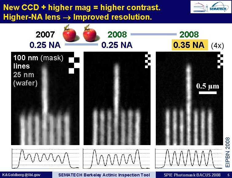
New CCD + higher mag = higher contrast. Higher-NA lens Improved resolution. 2007 0. 25 NA 2008 0. 35 NA (4 x) EIPBN 2008 100 nm (mask) lines 25 nm (wafer) KAGoldberg @ lbl. gov SEMATECH Berkeley Actinic Inspection Tool SPIE Photomask BACUS 2008 5
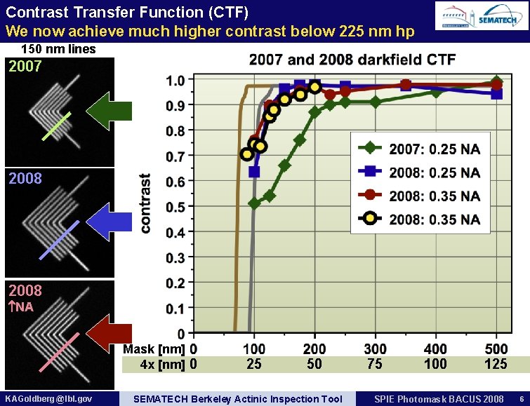
Contrast Transfer Function (CTF) We now achieve much higher contrast below 225 nm hp 150 nm lines 2007 2008 NA Mask [nm] 4 x [nm] 0 KAGoldberg @ lbl. gov 25 50 SEMATECH Berkeley Actinic Inspection Tool 75 100 125 SPIE Photomask BACUS 2008 6
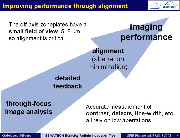
Improving performance through alignment The off-axis zoneplates have a small field of view, 5– 8 µm, so alignment is critical. imaging performance alignment (aberration minimization) detailed feedback through-focus image analysis KAGoldberg @ lbl. gov Accurate measurement of contrast, defects, line-width, etc. all rely on low aberrations. SEMATECH Berkeley Actinic Inspection Tool SPIE Photomask BACUS 2008 7
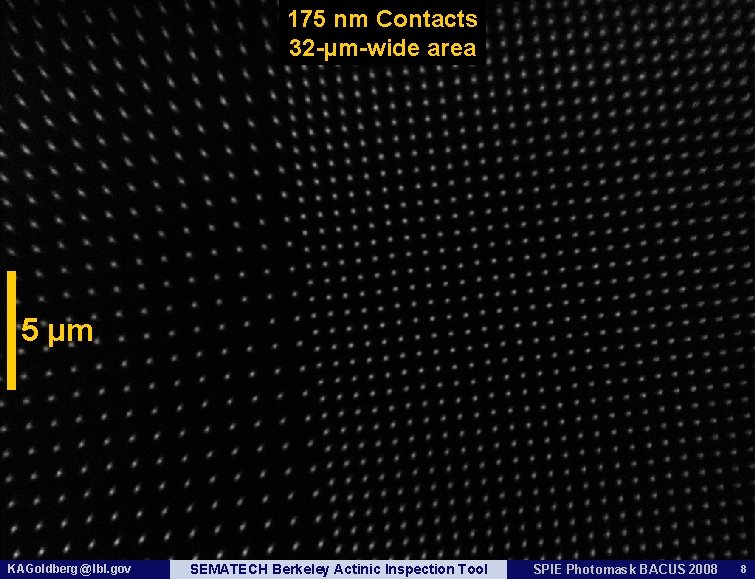
175 nm Contacts 32 -µm-wide area 5 µm KAGoldberg @ lbl. gov SEMATECH Berkeley Actinic Inspection Tool SPIE Photomask BACUS 2008 8
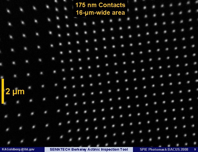
175 nm Contacts 16 -µm-wide area 2 µm KAGoldberg @ lbl. gov SEMATECH Berkeley Actinic Inspection Tool SPIE Photomask BACUS 2008 9
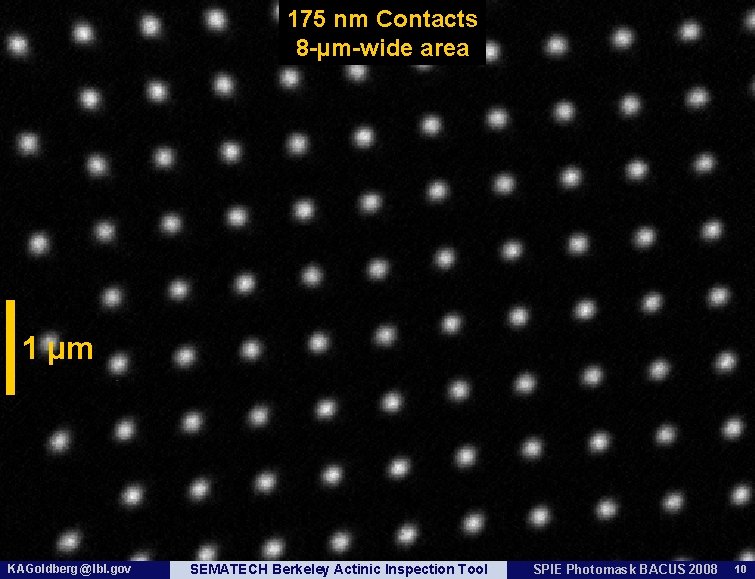
175 nm Contacts 8 -µm-wide area 1 µm KAGoldberg @ lbl. gov SEMATECH Berkeley Actinic Inspection Tool SPIE Photomask BACUS 2008 10
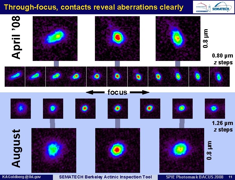
0. 8 µm April ’ 08 Through-focus, contacts reveal aberrations clearly 0. 80 µm z steps focus KAGoldberg @ lbl. gov 0. 8 µm August 1. 26 µm z steps SEMATECH Berkeley Actinic Inspection Tool SPIE Photomask BACUS 2008 11
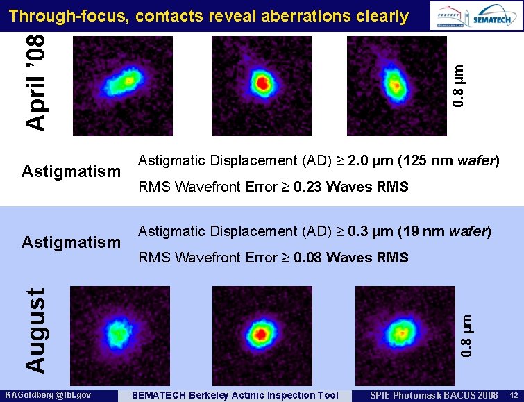
Astigmatism Astigmatic Displacement (AD) ≥ 2. 0 µm (125 nm wafer) RMS Wavefront Error ≥ 0. 23 Waves RMS Astigmatic Displacement (AD) ≥ 0. 3 µm (19 nm wafer) RMS Wavefront Error ≥ 0. 08 Waves RMS KAGoldberg @ lbl. gov 0. 8 µm August Astigmatism 0. 8 µm April ’ 08 Through-focus, contacts reveal aberrations clearly SEMATECH Berkeley Actinic Inspection Tool SPIE Photomask BACUS 2008 12
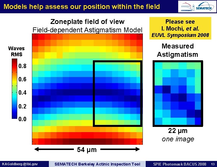
Models help assess our position within the field Zoneplate field of view Field-dependent Astigmatism Model Please see I. Mochi, et al. EUVL Symposium 2008 Measured Astigmatism Waves RMS 0. 8 0. 6 0. 4 0. 2 0. 0 22 µm one image 54 µm KAGoldberg @ lbl. gov SEMATECH Berkeley Actinic Inspection Tool SPIE Photomask BACUS 2008 13
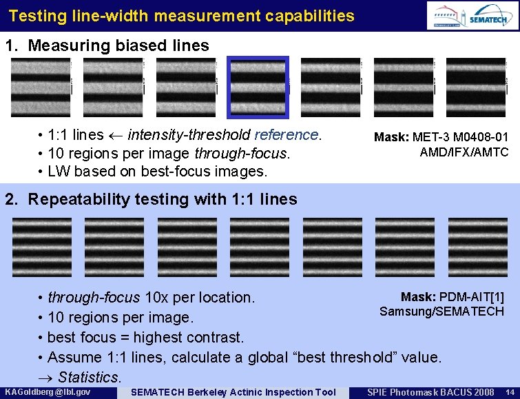
Testing line-width measurement capabilities 1. Measuring biased lines • 1: 1 lines intensity-threshold reference. • 10 regions per image through-focus. • LW based on best-focus images. Mask: MET-3 M 0408 -01 AMD/IFX/AMTC 2. Repeatability testing with 1: 1 lines Mask: PDM-AIT[1] • through-focus 10 x per location. Samsung/SEMATECH • 10 regions per image. • best focus = highest contrast. • Assume 1: 1 lines, calculate a global “best threshold” value. Statistics. KAGoldberg @ lbl. gov SEMATECH Berkeley Actinic Inspection Tool SPIE Photomask BACUS 2008 14
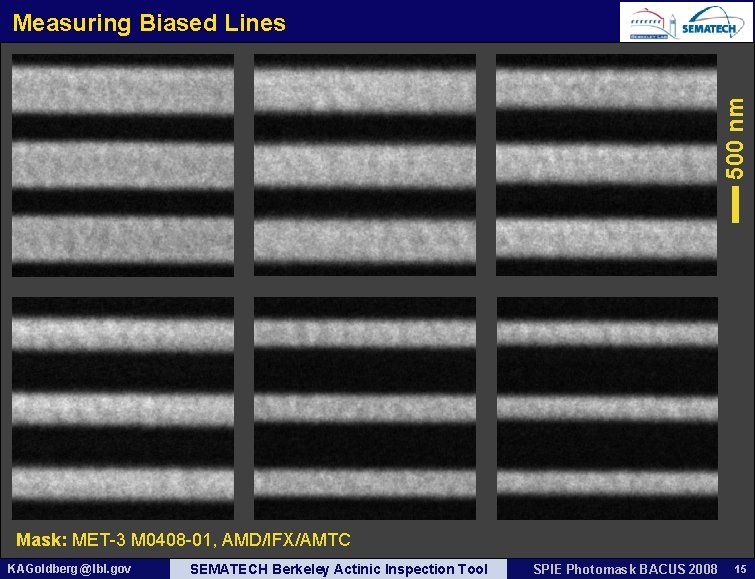
500 nm Measuring Biased Lines Mask: MET-3 M 0408 -01, AMD/IFX/AMTC KAGoldberg @ lbl. gov SEMATECH Berkeley Actinic Inspection Tool SPIE Photomask BACUS 2008 15
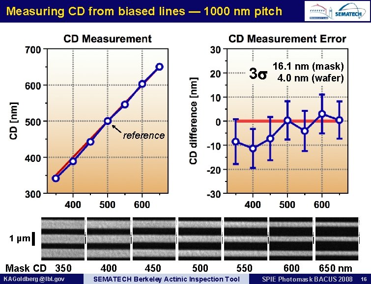
Measuring CD from biased lines — 1000 nm pitch 3 16. 1 nm (mask) 4. 0 nm (wafer) reference 1 µm Mask CD 350 KAGoldberg @ lbl. gov 400 450 500 550 SEMATECH Berkeley Actinic Inspection Tool 600 650 nm SPIE Photomask BACUS 2008 16
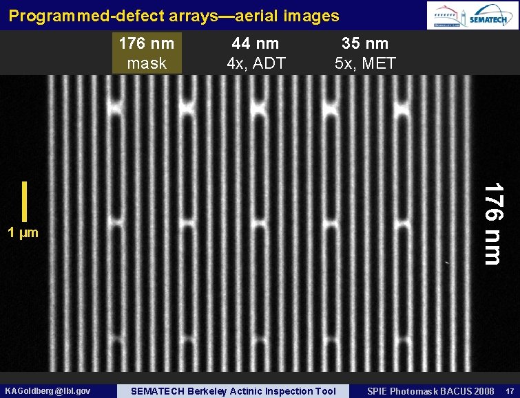
Programmed-defect arrays—aerial images 176 nm mask 44 nm 4 x, ADT 35 nm 5 x, MET 176 nm 1 µm KAGoldberg @ lbl. gov SEMATECH Berkeley Actinic Inspection Tool SPIE Photomask BACUS 2008 17
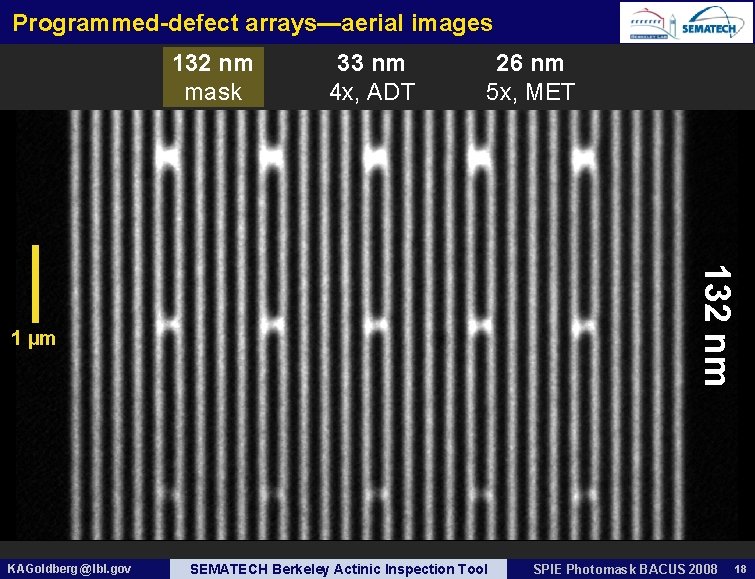
Programmed-defect arrays—aerial images 132 nm mask 33 nm 4 x, ADT 26 nm 5 x, MET 132 nm 1 µm KAGoldberg @ lbl. gov SEMATECH Berkeley Actinic Inspection Tool SPIE Photomask BACUS 2008 18
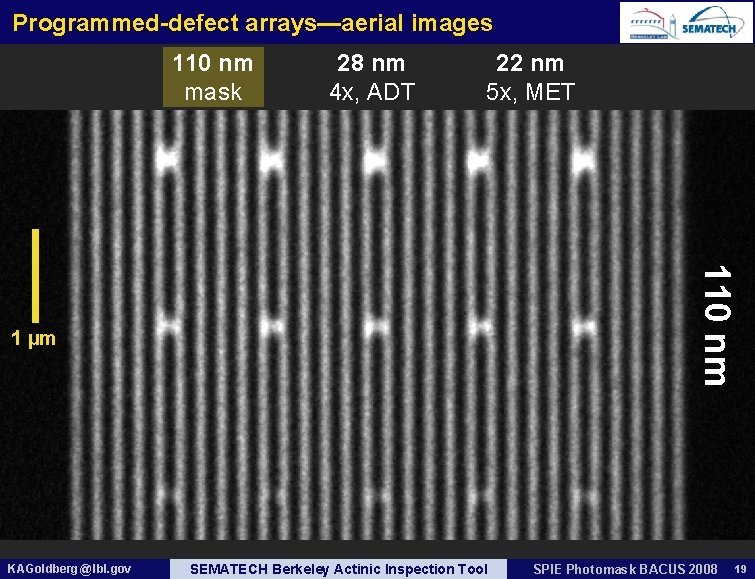
Programmed-defect arrays—aerial images 110 nm mask 28 nm 4 x, ADT 22 nm 5 x, MET 110 nm 1 µm KAGoldberg @ lbl. gov SEMATECH Berkeley Actinic Inspection Tool SPIE Photomask BACUS 2008 19
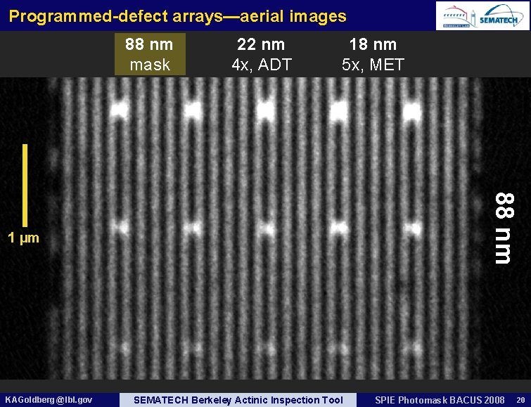
Programmed-defect arrays—aerial images 88 nm mask 22 nm 4 x, ADT 18 nm 5 x, MET 88 nm 1 µm KAGoldberg @ lbl. gov SEMATECH Berkeley Actinic Inspection Tool SPIE Photomask BACUS 2008 20
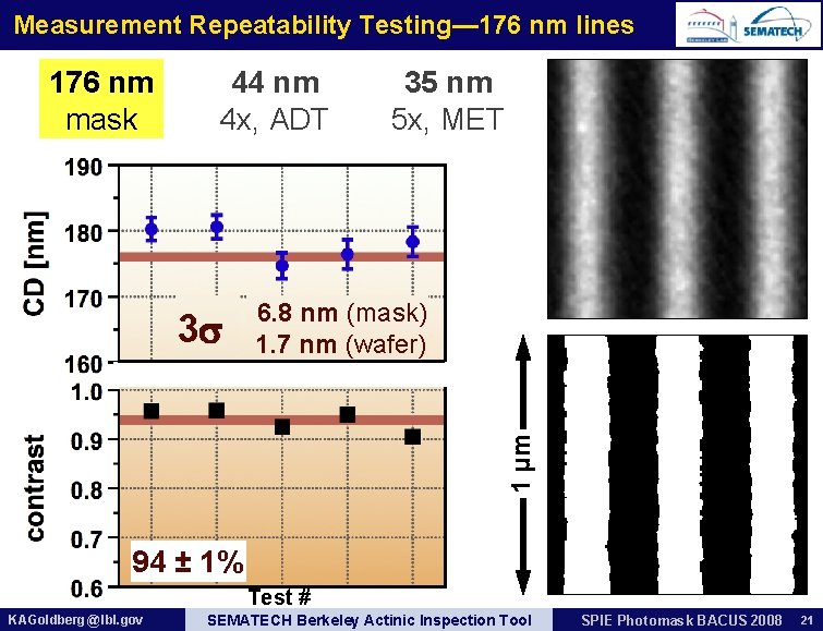
Measurement Repeatability Testing— 176 nm lines 176 nm mask 44 nm 4 x, ADT 6. 8 nm (mask) 1. 7 nm (wafer) 1 µm 3 35 nm 5 x, MET 94 ± 1% Test # KAGoldberg @ lbl. gov SEMATECH Berkeley Actinic Inspection Tool SPIE Photomask BACUS 2008 21
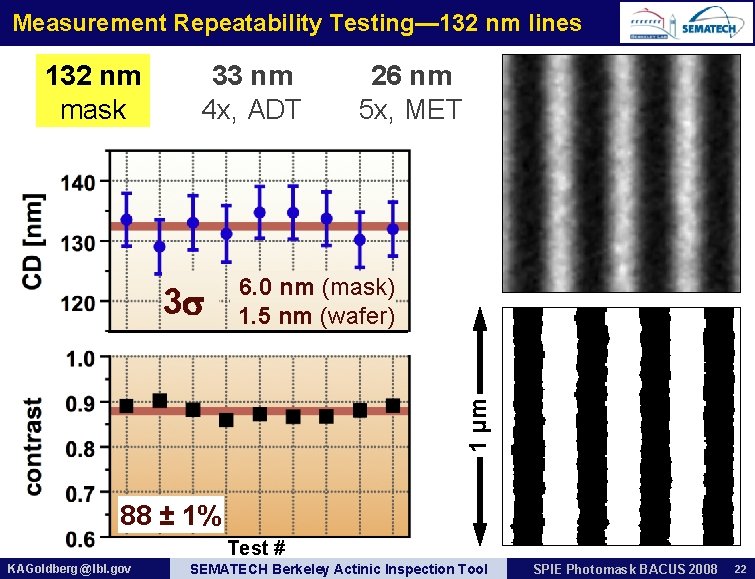
Measurement Repeatability Testing— 132 nm lines 132 nm mask 33 nm 4 x, ADT 6. 0 nm (mask) 1. 5 nm (wafer) 1 µm 3 26 nm 5 x, MET 88 ± 1% Test # KAGoldberg @ lbl. gov SEMATECH Berkeley Actinic Inspection Tool SPIE Photomask BACUS 2008 22
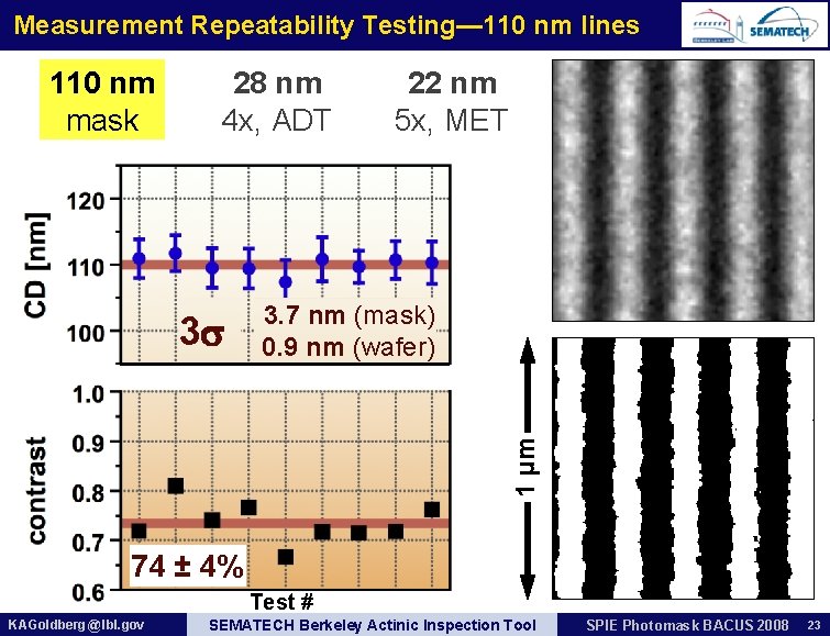
Measurement Repeatability Testing— 110 nm lines 110 nm mask 28 nm 4 x, ADT 3. 7 nm (mask) 0. 9 nm (wafer) 1 µm 3 22 nm 5 x, MET 74 ± 4% Test # KAGoldberg @ lbl. gov SEMATECH Berkeley Actinic Inspection Tool SPIE Photomask BACUS 2008 23
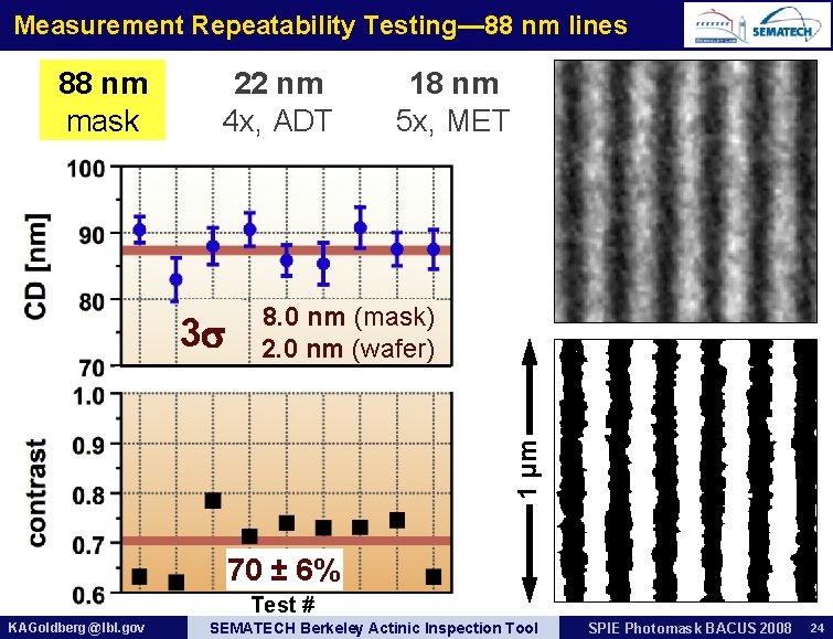
Measurement Repeatability Testing— 88 nm lines 88 nm mask 22 nm 4 x, ADT 8. 0 nm (mask) 2. 0 nm (wafer) 1 µm 3 18 nm 5 x, MET 70 ± 6% Test # KAGoldberg @ lbl. gov SEMATECH Berkeley Actinic Inspection Tool SPIE Photomask BACUS 2008 24
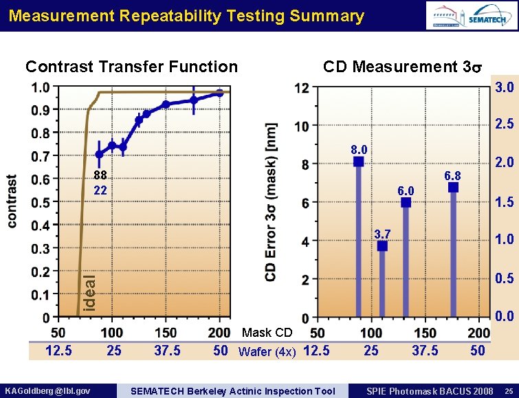
Measurement Repeatability Testing Summary Contrast Transfer Function CD Measurement 3 3. 0 2. 5 8. 0 88 22 2. 0 6. 8 6. 0 1. 5 3. 7 1. 0 ideal 0. 5 0. 0 Mask CD 12. 5 KAGoldberg @ lbl. gov 25 37. 5 50 Wafer (4 x) 12. 5 SEMATECH Berkeley Actinic Inspection Tool 25 37. 5 50 SPIE Photomask BACUS 2008 25
![Through-focus analysis of 180 nm CD (mask) lines Defocus Z [µm] best LW Uncertainty Through-focus analysis of 180 nm CD (mask) lines Defocus Z [µm] best LW Uncertainty](http://slidetodoc.com/presentation_image_h/b7ed85a35644a32573310d7da15e8177/image-26.jpg)
Through-focus analysis of 180 nm CD (mask) lines Defocus Z [µm] best LW Uncertainty 3 nm KAGoldberg @ lbl. gov SEMATECH Berkeley Actinic Inspection Tool SPIE Photomask BACUS 2008 26
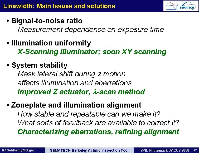
Linewidth: Main Issues and solutions • Signal-to-noise ratio Measurement dependence on exposure time • Illumination uniformity X-Scanning illuminator; soon XY scanning • System stability Mask lateral shift during z motion affects illumination and aberrations Improved Z actuator, -scan method • Zoneplate and illumination alignment How stable and repeatable can we make it? What sorts of feedback are available to correct it? Characterizing aberrations, refining alignment KAGoldberg @ lbl. gov SEMATECH Berkeley Actinic Inspection Tool SPIE Photomask BACUS 2008 27
Conclusion • System upgrades: improved resolution, contrast, 0. 35 NA (4 x) • Aberrations: reduced by alignment & analysis Astigmatism is down, from 0. 23 to 0. 08 RMS • Contrast: 71% for 88 -nm lines (22 nm 4 x) • Linewidth 3 : Repeatability ~5 nm 3 (1. 25 nm on wafer) • More improvements will come from a combination of hardware & software solutions. KAGoldberg @ lbl. gov SEMATECH Berkeley Actinic Inspection Tool SPIE Photomask BACUS 2008 28
Special Thanks! CXRO David Attwood Seno Rekawa Drew Kemp Nathan Smith Paul Denham Erik Anderson Bob Gunion Eric Gullikson Ron Tackaberry 1 µm For More Information: http: //Goldberg. LBL. Gov KAGoldberg @ lbl. gov SEMATECH Berkeley Actinic Inspection Tool SPIE Photomask BACUS 2008 29
- Slides: 29