
BEE 3 Update Chuck Thacker Technical Fellow Microsoft
BEE 3 Update Chuck Thacker Technical Fellow Microsoft Research 11 January, 2007
Outline • • What is BEE 3? BEE 2 -BEE 3 Differences Project participants Engineering plan, schedule

What is BEE 3? • Follow-on to BEE 2 (BWRC, 2004) • Board with several highly-connected FPGAs • Vehicle for computer architecture research – Microsoft’s primary interest • Potential platform for high performance DSP applications – Astronomers, and perhaps others. • Allows large scale architectural experiments – Although perhaps not as large as originally hoped – And certainly not at the speed of a real implementation • Can scale smoothly from a single board to 64 boards (256 FPGAs)

BEE 2
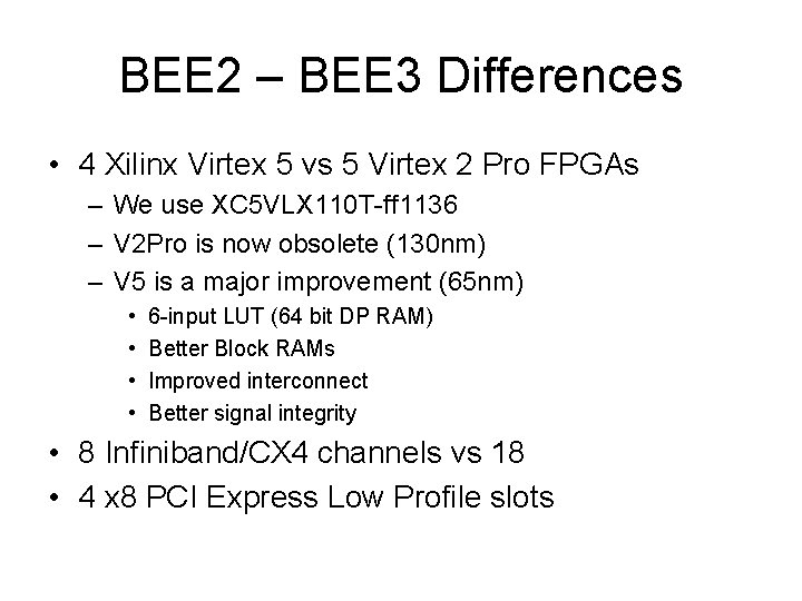
BEE 2 – BEE 3 Differences • 4 Xilinx Virtex 5 vs 5 Virtex 2 Pro FPGAs – We use XC 5 VLX 110 T-ff 1136 – V 2 Pro is now obsolete (130 nm) – V 5 is a major improvement (65 nm) • • 6 -input LUT (64 bit DP RAM) Better Block RAMs Improved interconnect Better signal integrity • 8 Infiniband/CX 4 channels vs 18 • 4 x 8 PCI Express Low Profile slots
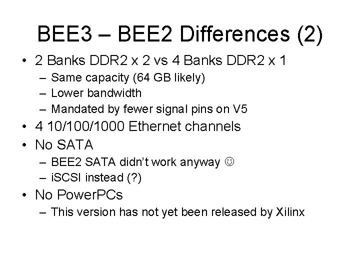
BEE 3 – BEE 2 Differences (2) • 2 Banks DDR 2 x 2 vs 4 Banks DDR 2 x 1 – Same capacity (64 GB likely) – Lower bandwidth – Mandated by fewer signal pins on V 5 • 4 10/1000 Ethernet channels • No SATA – BEE 2 SATA didn’t work anyway – i. SCSI instead (? ) • No Power. PCs – This version has not yet been released by Xilinx
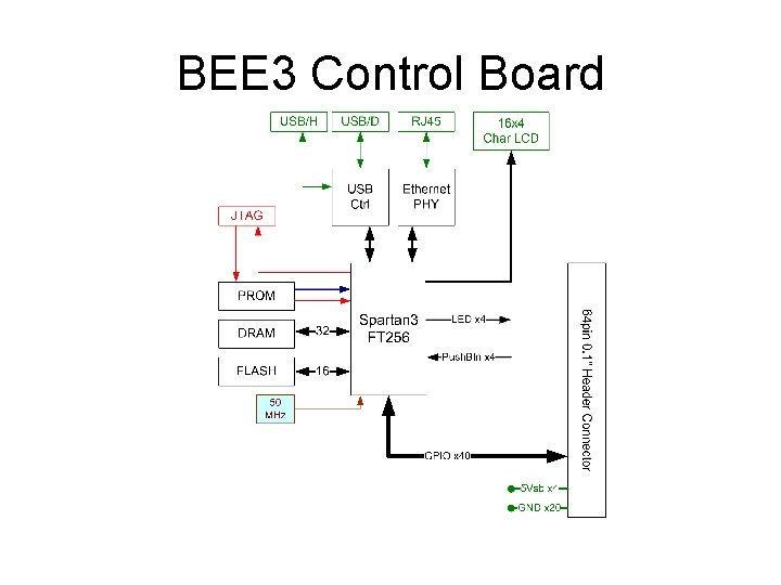
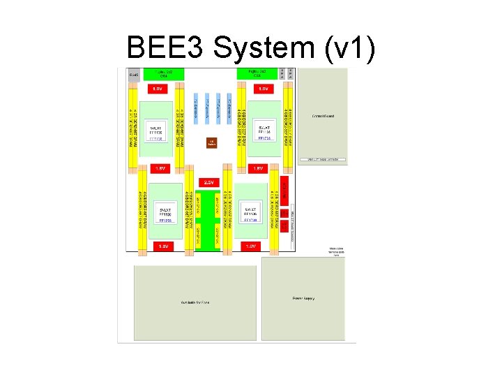
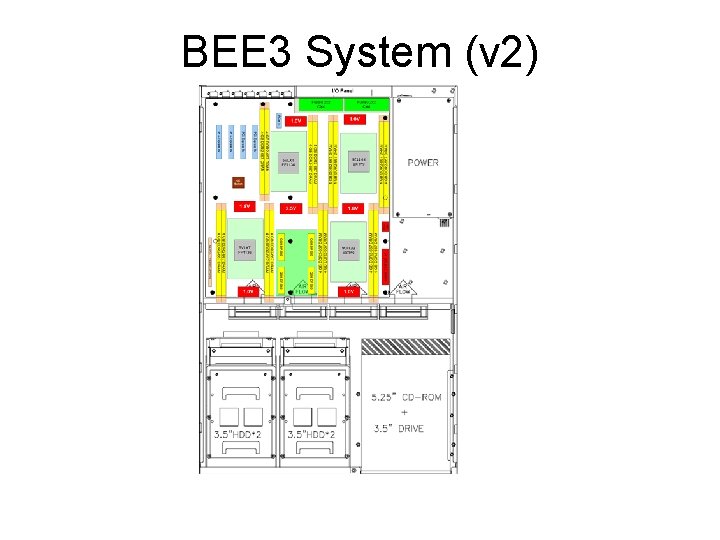
BEE 2 – BEE 3 Differences (3) • Divided the system into two boards, Main and Control – Main board has FPGAs, all high speed logic – Control board handles downloading, monitoring – Simplifies main board engineering – can design control board in parallel • Smaller main board – 168 vs 374 in 2 – Fewer layers for lower cost • Much more “PC-like” • Can use PC power supplies, peripherals • Several layouts are being considered – All fit in 2 U enclosure – Much more attention is being given to thermal design – Must pass UL, FCC
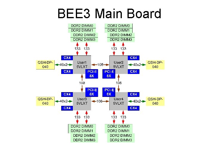
BEE 3 Main Board
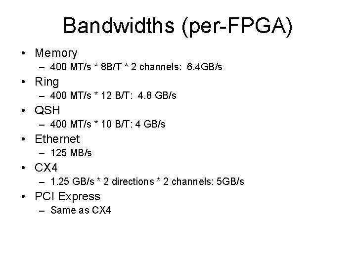
Bandwidths (per-FPGA) • Memory – 400 MT/s * 8 B/T * 2 channels: 6. 4 GB/s • Ring – 400 MT/s * 12 B/T: 4. 8 GB/s • QSH – 400 MT/s * 10 B/T: 4 GB/s • Ethernet – 125 MB/s • CX 4 – 1. 25 GB/s * 2 directions * 2 channels: 5 GB/s • PCI Express – Same as CX 4
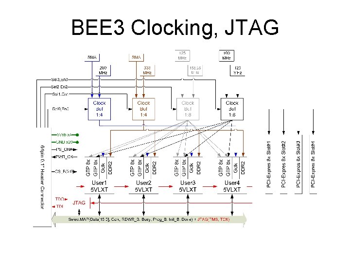
BEE 3 Clocking, JTAG
BEE 3 Control Board
BEE 3 System (v 1)
BEE 3 System (v 2)

BEE 3 Main Board (v 3)
Remaining Issues • Precise EATX compatibility, or not? – Affects layout complexity, thermal design • Power supply sizing – We don’t want to leave the overclockers in the lurch • Standard power supplies (? ) – “ 2 U” supplies aren’t as efficient, have fewer vendors – Prefer Intel/Google “ 12 V only” supplies (minimum loading issue), if available in time and at reasonable cost • PCI Express is nonstandard – Xilinx hard macro is “device only”, not host – Need an intrepid graduate student – Can still use it for additional Infiniband/CX 4 channels

Project Participants and Roles • Microsoft Research (Silicon Valley) – Funds and manages system engineering • Celestica (Ottawa and elsewhere) – Does main board engineering, produces final systems – Microsoft has a very deep relationship with Celestica • Function Engineering (Palo Alto) – Does thermal and mechanical engineering • Xilinx (San Jose) – Provides FPGAs for academic machines – Provides FPGA application expertise • Ramp Group (BWRC) – Control board, basic software • Ramp Community – Uses the systems for research

Why is Microsoft interested? • We believe the overall RAMP effort will have significant impact, and want to support it in the most effective way we can. – Simply paying for grad students seems suboptimal • We observe that universities aren’t very good at this sort of system engineering and production – Grad students are great for many things, but doing things like board layout aren’t among them. – Requires deep understanding of tools and production processes. Pros have this. – We can open doors that academia can’t – We have experience in managing this sort of program • We want the systems ourselves – As infrastructure for our new effort in computer architecture (yes, this is a recruiting pitch). • We also want systems to be available to other industrial users – This might be more difficult if the systems came from academia. – But we don’t want to be in the hardware business.
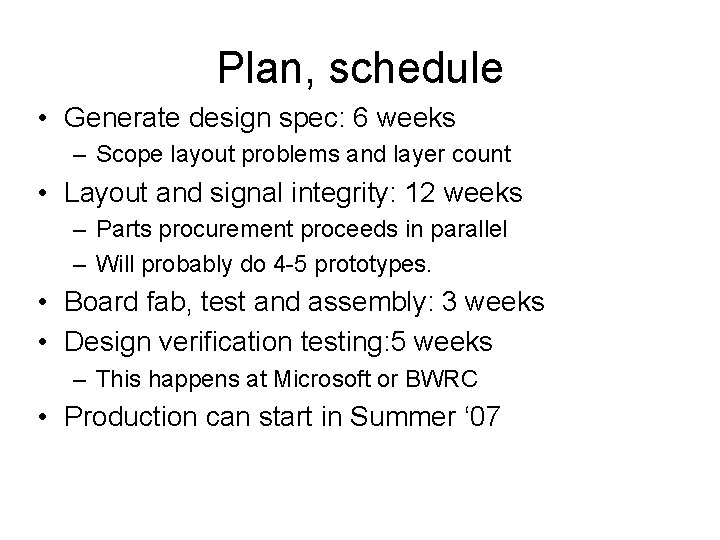
Plan, schedule • Generate design spec: 6 weeks – Scope layout problems and layer count • Layout and signal integrity: 12 weeks – Parts procurement proceeds in parallel – Will probably do 4 -5 prototypes. • Board fab, test and assembly: 3 weeks • Design verification testing: 5 weeks – This happens at Microsoft or BWRC • Production can start in Summer ‘ 07

Discussion?
- Slides: 19