BCC Buffer Control Chip Rough Document David Nelson
BCC Buffer Control Chip Rough Document David Nelson (SLAC), Matt Warren (UCL)
Change Log • 2009 -02 -24: Born as talk for Upgrade Week • 2009 -03 -18: Reworked as document (for now) – Fixed Readout diag to show ffs post-mux – Updated L 1 R decoding info – More detail on COM data format – Added info Confreg bits 13, 14, 15 – Tidied l 1 r/com descriptions 19/03/09 BCC Rough Document 2
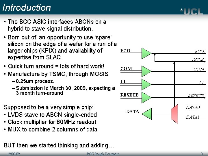
Introduction • The BCC ASIC interfaces ABCNs on a hybrid to stave signal distribution. • Born out of an opportunity to use ‘spare’ silicon on the edge of a wafer for a run of a larger chips (KPIX) and availability of expertise from SLAC. • Quick turn around = lots of hard work! • Manufacture by TSMC, through MOSIS BCO DCLK COM – 0. 25 um process. L 1 – Submission is March 30, 2009, expecting a 3 month turn-around RESETB Supposed to be a very simple chip: • LVDS stave to ABCN single-ended • Clock multiplier for 80 MHz readout • MUX to combine 2 columns of data BCO DATA COM L 1 RESETB DATA 0 DATA 1 BUT then we started thinking and adding… 19/03/09 BCC Rough Document 3
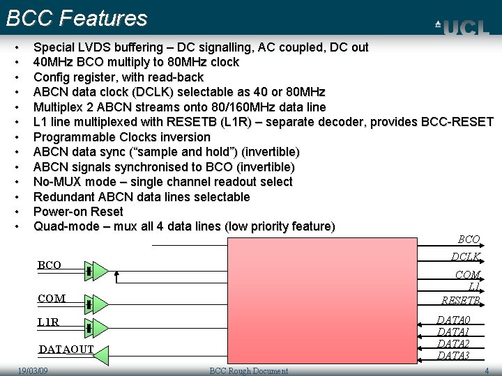
BCC Features • • • • Special LVDS buffering – DC signalling, AC coupled, DC out 40 MHz BCO multiply to 80 MHz clock Config register, with read-back ABCN data clock (DCLK) selectable as 40 or 80 MHz Multiplex 2 ABCN streams onto 80/160 MHz data line L 1 line multiplexed with RESETB (L 1 R) – separate decoder, provides BCC-RESET Programmable Clocks inversion ABCN data sync (“sample and hold”) (invertible) ABCN signals synchronised to BCO (invertible) No-MUX mode – single channel readout select Redundant ABCN data lines selectable Power-on Reset Quad-mode – mux all 4 data lines (low priority feature) BCO DCLK BCO COM L 1 RESETB COM DATA 0 DATA 1 DATA 2 DATA 3 L 1 R DATAOUT 19/03/09 BCC Rough Document 4

‘Special’ LVDS DC-AC-DC Buffer • • DC Signals are AC coupled Feedback is used to ‘hold’ the level beyond the RC constant Passives are external to BCC for tuning Feedback resistors are set by two requirements: –The LVDS receiver needs >100 m. V on input in the static condition Value set to 150 m. V to guarantee properation. Could be reduced by 2 with MLVDS –Total input impedance as high as possible for parallel operation (driving several hybrids) The capacitors as set as small as possible to reduce stored energy • The data rate is limited by having two LVDS circuits in series in a feedback mode RF Stave LVDS 100 R RF 19/03/09 BCC Rough Document 5
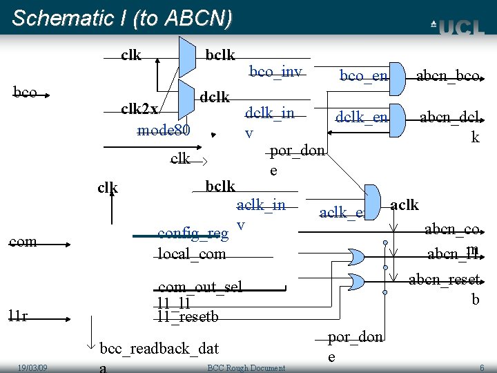
Schematic I (to ABCN) clk bco bclk 2 x mode 80 bco_inv dclk clk com l 1 r bclk config_reg local_com bco_en abcn_bco dclk_in dclk_en v por_don e abcn_dcl k aclk_in v BCC Rough Document aclk abcn_co m abcn_l 1 abcn_reset b com_out_sel l 1_l 1 l 1_resetb bcc_readback_dat 19/03/09 aclk_en por_don e 6
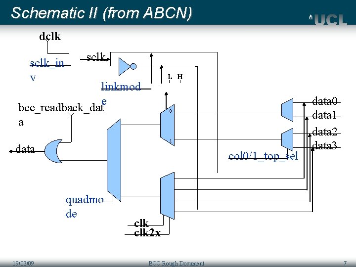
Schematic II (from ABCN) dclk sclk_in v sclk L H linkmod e bcc_readback_dat a 0 1 data col 0/1_top_sel quadmo de 19/03/09 data 0 data 1 data 2 data 3 clk 2 x BCC Rough Document 7
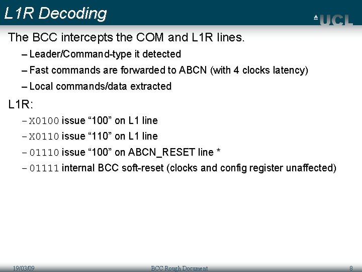
L 1 R Decoding The BCC intercepts the COM and L 1 R lines. – Leader/Command-type it detected – Fast commands are forwarded to ABCN (with 4 clocks latency) – Local commands/data extracted L 1 R: – X 0100 issue “ 100” on L 1 line – X 0110 issue “ 110” on L 1 line – 01110 issue “ 100” on ABCN_RESET line * – 01111 internal BCC soft-reset (clocks and config register unaffected) 19/03/09 BCC Rough Document 8
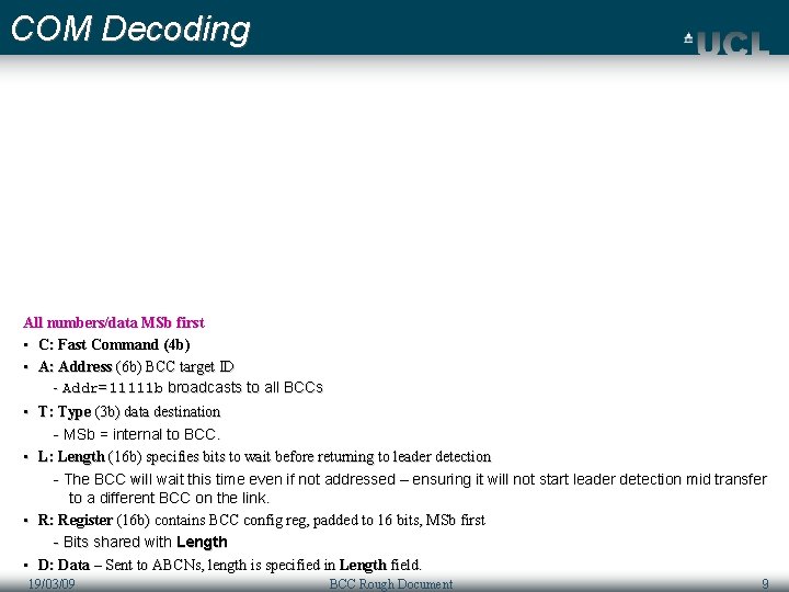
COM Decoding All numbers/data MSb first • C: Fast Command (4 b) • A: Address (6 b) BCC target ID - Addr=11111 b broadcasts to all BCCs • T: Type (3 b) data destination - MSb = internal to BCC. • L: Length (16 b) specifies bits to wait before returning to leader detection - The BCC will wait this time even if not addressed – ensuring it will not start leader detection mid transfer to a different BCC on the link. • R: Register (16 b) contains BCC config reg, padded to 16 bits, MSb first - Bits shared with Length • D: Data – Sent to ABCNs, length is specified in Length field. 19/03/09 BCC Rough Document 9
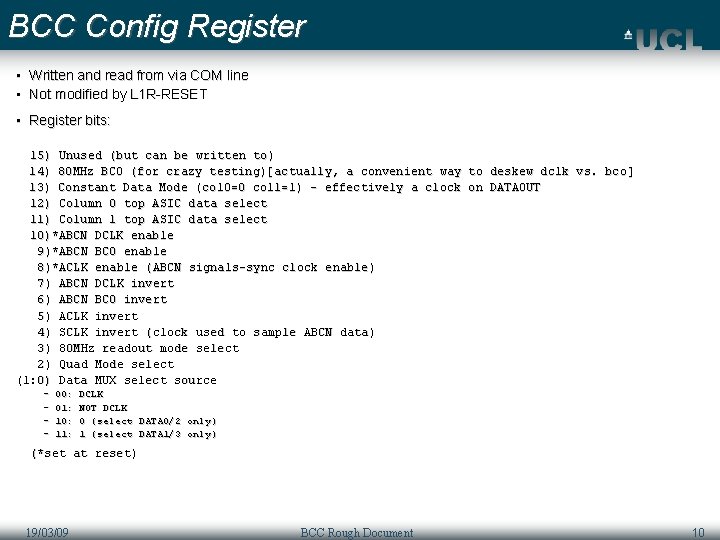
BCC Config Register • Written and read from via COM line • Not modified by L 1 R-RESET • Register bits: 15) Unused (but can be written to) 14) 80 MHz BCO (for crazy testing)[actually, a convenient way to deskew dclk vs. bco] 13) Constant Data Mode (col 0=0 col 1=1) – effectively a clock on DATAOUT 12) Column 0 top ASIC data select 11) Column 1 top ASIC data select 10)*ABCN DCLK enable 9)*ABCN BCO enable 8)*ACLK enable (ABCN signals-sync clock enable) 7) ABCN DCLK invert 6) ABCN BCO invert 5) ACLK invert 4) SCLK invert (clock used to sample ABCN data) 3) 80 MHz readout mode select 2) Quad Mode select (1: 0) Data MUX select source - 00: 01: 10: 11: DCLK NOT DCLK 0 (select DATA 0/2 only) 1 (select DATA 1/3 only) (*set at reset) 19/03/09 BCC Rough Document 10
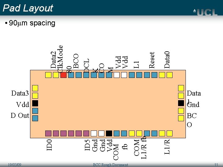
Pad Layout Data 0 Reset L 1 Data 2 Clk. Mode 80 BCO DCL K CO M Vdd • 90μm spacing Data 1 Gnd Data 3 Vdd D Out 19/03/09 BCC Rough Document L 1/R COM L 1/R fb ID 5 Gnd Vdd COM fb ID 0 BC O 11
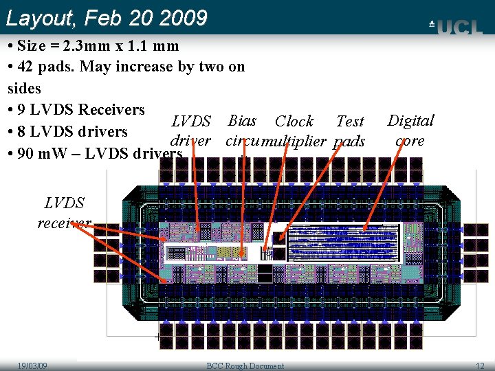
Layout, Feb 20 2009 • Size = 2. 3 mm x 1. 1 mm • 42 pads. May increase by two on sides • 9 LVDS Receivers LVDS Bias Clock Test • 8 LVDS drivers driver circu multiplier pads • 90 m. W – LVDS drivers it Digital core LVDS receiver 19/03/09 BCC Rough Document 12
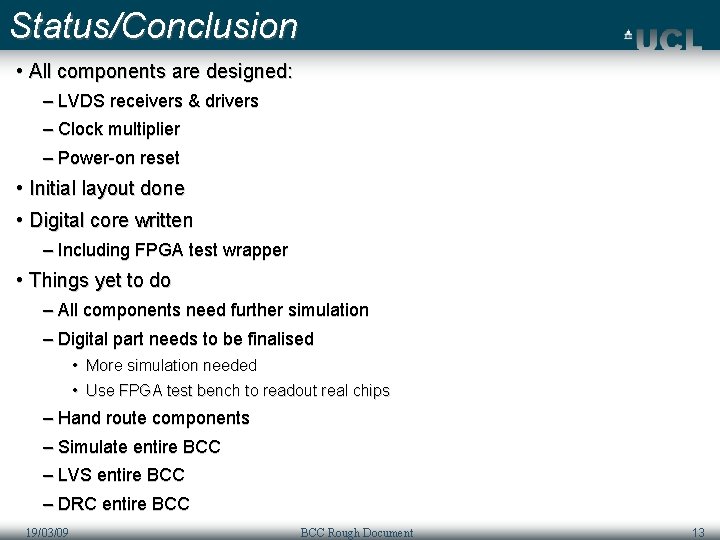
Status/Conclusion • All components are designed: – LVDS receivers & drivers – Clock multiplier – Power-on reset • Initial layout done • Digital core written – Including FPGA test wrapper • Things yet to do – All components need further simulation – Digital part needs to be finalised • More simulation needed • Use FPGA test bench to readout real chips – Hand route components – Simulate entire BCC – LVS entire BCC – DRC entire BCC 19/03/09 BCC Rough Document 13
- Slides: 13