
Battery Voltage Boost Regulator Solving the Mary Gomez
Battery Voltage Boost Regulator Solving the Mary Gomez Park Incident Don Steinbach, AE 6 PM 1
The Mary Gomez Park Incident • Yaesu FT-840 transceiver received bad (terrible) signal quality reports on CW after being operated on battery power for an extended period of time. • Believed to be a result of the dc input voltage being out-of-spec low. – Actual battery voltage was near 11 V – FT-840 Spec is 13. 5 V +/- 10% (12. 15 to 14. 85) Don Steinbach, AE 6 PM 2
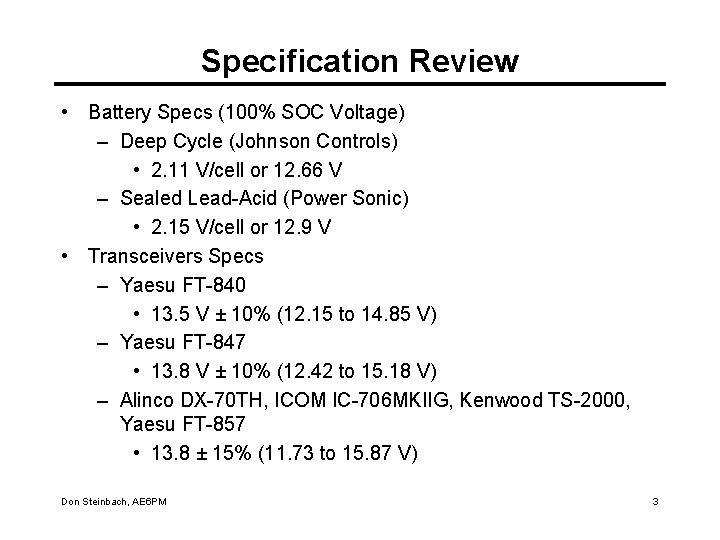
Specification Review • Battery Specs (100% SOC Voltage) – Deep Cycle (Johnson Controls) • 2. 11 V/cell or 12. 66 V – Sealed Lead-Acid (Power Sonic) • 2. 15 V/cell or 12. 9 V • Transceivers Specs – Yaesu FT-840 • 13. 5 V ± 10% (12. 15 to 14. 85 V) – Yaesu FT-847 • 13. 8 V ± 10% (12. 42 to 15. 18 V) – Alinco DX-70 TH, ICOM IC-706 MKIIG, Kenwood TS-2000, Yaesu FT-857 • 13. 8 ± 15% (11. 73 to 15. 87 V) Don Steinbach, AE 6 PM 3
Possible Solutions • Add a second battery (or a cell) in series with the primary battery – Raise primary battery dc voltage to 14 or 18 or 24 volts and regulate down to 13 V • Use a modified/enhanced computer UPS – Let the primary battery power the UPS and let the UPS power the transceiver ac power supply • Use a dc/dc converter and regulator – Use a conventional dc/dc converter to provide 18 V then regulate down to 13 V • Use a boost supply in series with the battery – Add a differential voltage to the primary battery voltage Don Steinbach, AE 6 PM 4
QST to the Rescue • QST Article – A 12 V dc Boost Regulator for Battery Operation • Daniel R. Kemppainen, N 8 XJK • November 2004, page 37 Quote from the article: “A dc-dc boost switching converter is the answer to low voltage battery problems for mobile, portable or emergency-power operation” Don Steinbach, AE 6 PM 5
Step 1 – Check the Current Status • Contacted the author regarding availability of bare PC board – Author responded that circuit had been redesigned and that farcircuits had PC boards for sale • www. farcircuits. net – Author also stated that he has uploaded the new design to the ARRL website • www. arrl. org/files/qst-binaries/ Don Steinbach, AE 6 PM 6
Step 2 – Build It • Procure the PC board and the components – FAR Circuits • PCB, E-core and bobbin, toroid core – Digikey • Filter capacitors, power MOSFETs, Schottkey dual diode • Anything that needs to fit the PCB layout – Anchor Electronics • Miscellaneous ICs, semiconductors, resistors, capacitors • Wind the transformer • Wind the filter inductor • Stuff and solder the PC board • Cut, bend and drill some aluminum • Final electrical/mechanical assembly and heat sinking • Test 7
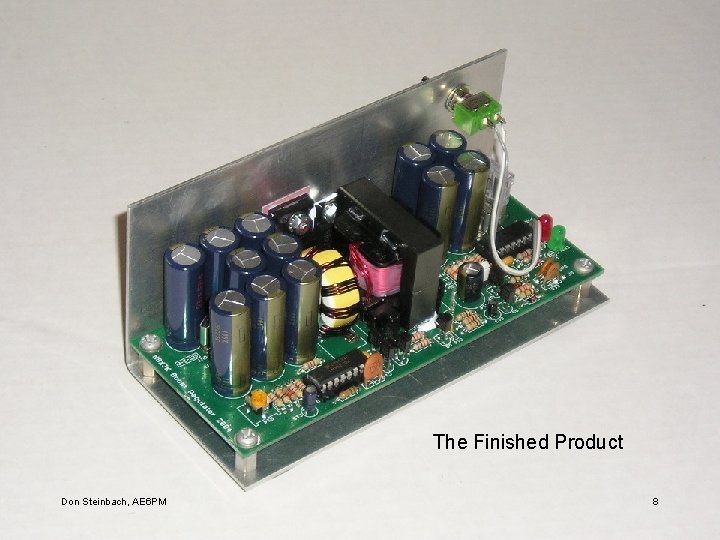
The Finished Product Don Steinbach, AE 6 PM 8
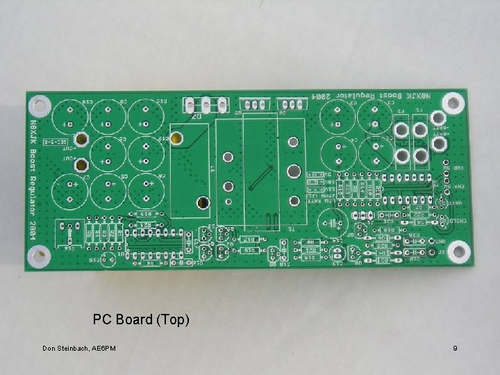
PCB Top PC Board (Top) Don Steinbach, AE 6 PM 9
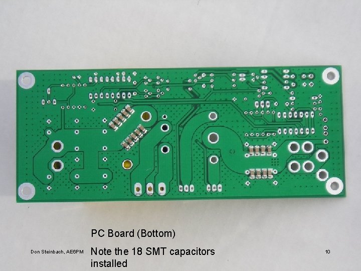
PCB Bottom PC Board (Bottom) Don Steinbach, AE 6 PM Note the 18 SMT capacitors installed 10
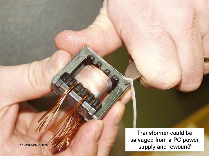
Don Steinbach, AE 6 PM Transformer could be salvaged from a PC power supply and rewound 11
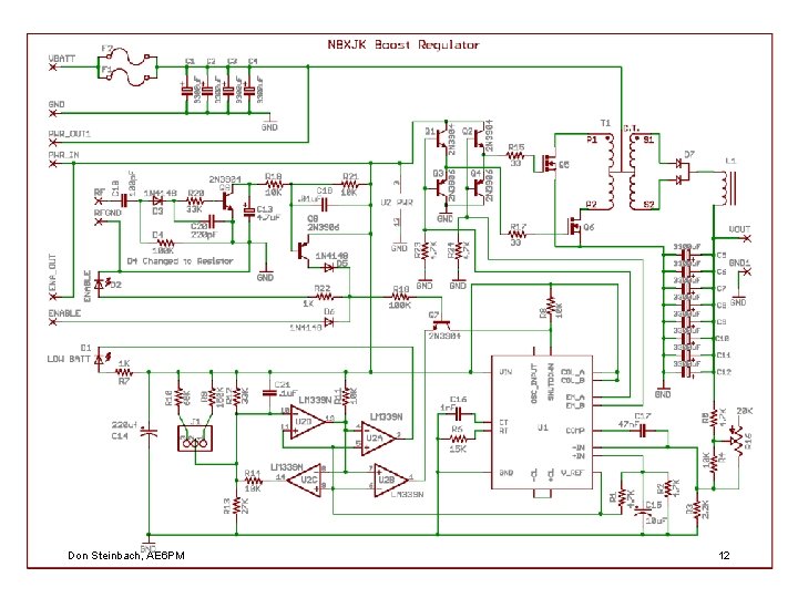
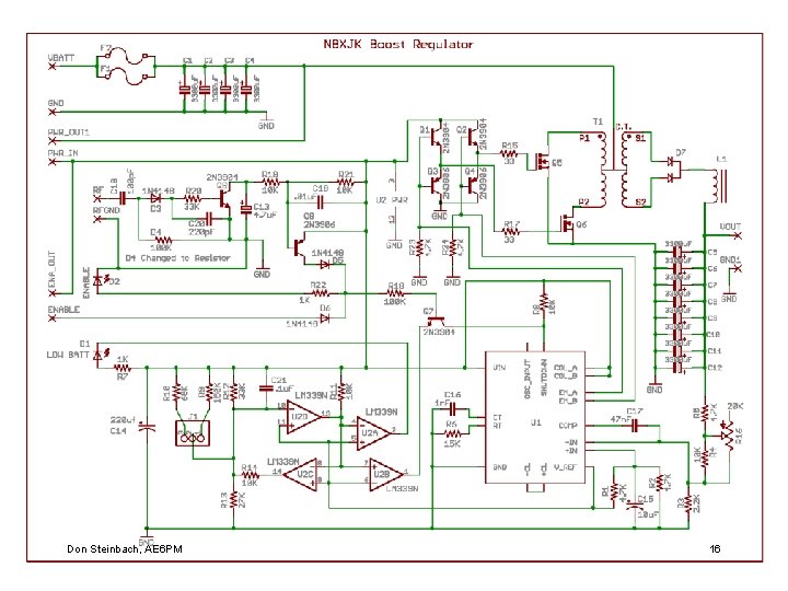
N 8 XJK Schematic Don Steinbach, AE 6 PM 12
Power Supply 101 Don Steinbach, AE 6 PM 13
Battery Boost Configuration Don Steinbach, AE 6 PM 14
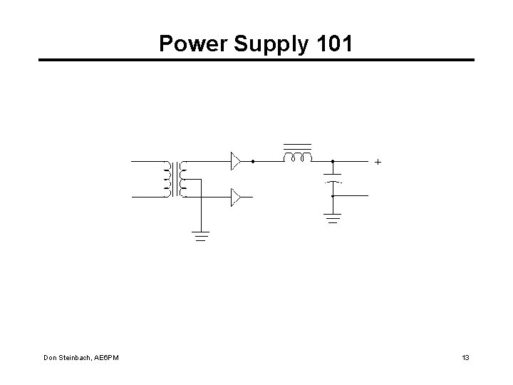
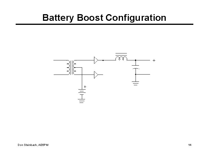
N 8 XJK Design Concept • The circuit is best visualized starting with a full-wave power supply using a transformer with a center tapped secondary. • The center tap, rather than being grounded, is connected to the high side of the battery so that the power supply adds to the battery voltage. • Feedback from the total output voltage back to the full-wave power supply causes the power supply to modulate its output voltage to keep the sum of the battery voltage plus the power supply voltage constant. • The power supply that supplies the additional voltage is a switch -mode design that operates from the same battery that is supplying the baseline power. • The IC that drives the switch-mode power supply provides the regulation by modulating the pulse width. Don Steinbach, AE 6 PM 15
N 8 XJK Schematic Don Steinbach, AE 6 PM 16
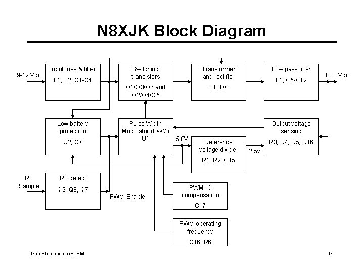
N 8 XJK Block Diagram 9 -12 Vdc Input fuse & filter F 1, F 2, C 1 -C 4 Low battery protection U 2, Q 7 Switching transistors Transformer and rectifier Q 1/Q 3/Q 6 and Q 2/Q 4/Q 5 T 1, D 7 Pulse Width Modulator (PWM) U 1 Low pass filter L 1, C 5 -C 12 13. 8 Vdc Output voltage sensing 5. 0 V Reference voltage divider R 3, R 4, R 5, R 16 2. 5 V R 1, R 2, C 15 RF Sample RF detect Q 9, Q 8, Q 7 PWM Enable PWM IC compensation C 17 PWM operating frequency C 16, R 6 Don Steinbach, AE 6 PM 17
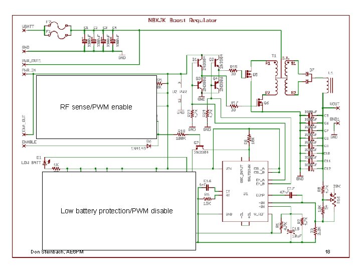
N 8 XJK Schematic (simplified) RF sense/PWM enable Low battery protection/PWM disable Don Steinbach, AE 6 PM 18
User Comments/Modification • Battery protection circuit – Reacts too quickly (false alarms) – Can only be reset by removing input power • RF detection/enable – Boost power supply turned on only during transmit • Different voltage during transmit and receive • Not recommended IMHO – Quiescent current is only 22 m. A I disabled battery protection & RF detection by removing U 2 and grounding emitter of Q 7 (jumper U 2 -1 to U 2 -12) Don Steinbach, AE 6 PM 19
Test Results • Test Duration: 6 minutes, continuous – Input Voltage: 12. 16 V dc – Output Voltage: 13. 0 V dc – Output Current: 16 A dc • Maximum Temperatures (IR Thermometer): – Transformer: 145 deg F – Diode area: 180 deg F – Heat sink area: Very hot to touch – Filter capacitors: Slightly warm • Switching Frequency: 40 k. Hz • Ripple voltage: 17 m. V p-p Don Steinbach, AE 6 PM 20
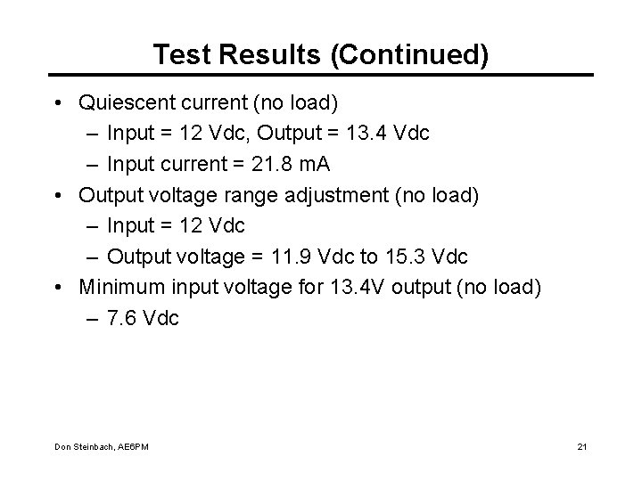
Test Results (Continued) • Quiescent current (no load) – Input = 12 Vdc, Output = 13. 4 Vdc – Input current = 21. 8 m. A • Output voltage range adjustment (no load) – Input = 12 Vdc – Output voltage = 11. 9 Vdc to 15. 3 Vdc • Minimum input voltage for 13. 4 V output (no load) – 7. 6 Vdc Don Steinbach, AE 6 PM 21
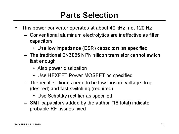
Parts Selection • This power converter operates at about 40 k. Hz, not 120 Hz – Conventional aluminum electrolytics are ineffective as filter capacitors • Use low impedance (ESR) capacitors as specified – The traditional 2 N 3055 NPN silicon transistor cannot switch fast enough • Also power dissipation • Use HEXFET Power MOSFET as specified – The rectifier diodes need to be low forward voltage drop (desired) and fast switching (required) • Use Schottky rectifier as specified – SMT capacitors added by the author (18 total) indicate probable RFI issues fixed Don Steinbach, AE 6 PM 22
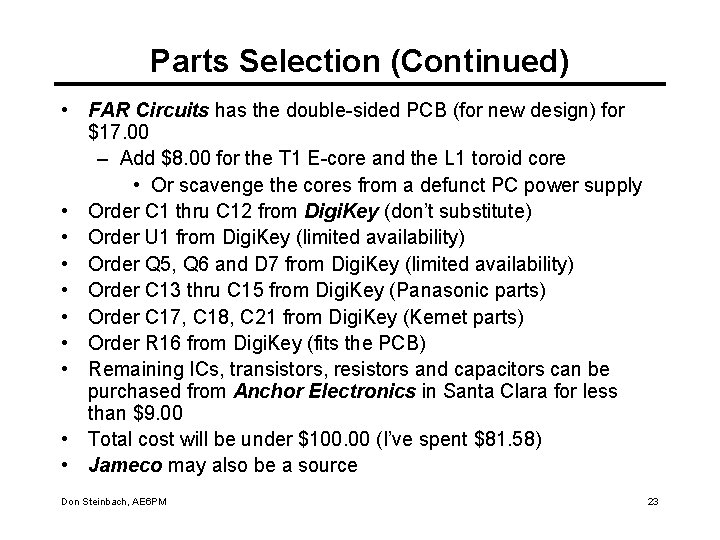
Parts Selection (Continued) • FAR Circuits has the double-sided PCB (for new design) for $17. 00 – Add $8. 00 for the T 1 E-core and the L 1 toroid core • Or scavenge the cores from a defunct PC power supply • Order C 1 thru C 12 from Digi. Key (don’t substitute) • Order U 1 from Digi. Key (limited availability) • Order Q 5, Q 6 and D 7 from Digi. Key (limited availability) • Order C 13 thru C 15 from Digi. Key (Panasonic parts) • Order C 17, C 18, C 21 from Digi. Key (Kemet parts) • Order R 16 from Digi. Key (fits the PCB) • Remaining ICs, transistors, resistors and capacitors can be purchased from Anchor Electronics in Santa Clara for less than $9. 00 • Total cost will be under $100. 00 (I’ve spent $81. 58) • Jameco may also be a source Don Steinbach, AE 6 PM 23
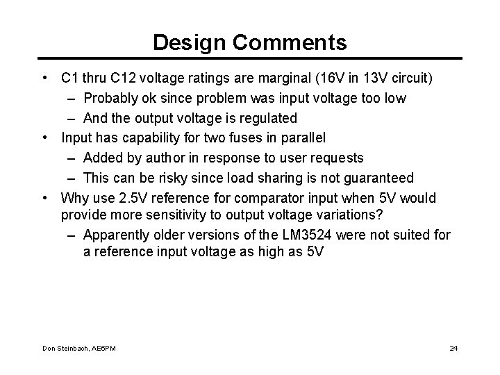
Design Comments • C 1 thru C 12 voltage ratings are marginal (16 V in 13 V circuit) – Probably ok since problem was input voltage too low – And the output voltage is regulated • Input has capability for two fuses in parallel – Added by author in response to user requests – This can be risky since load sharing is not guaranteed • Why use 2. 5 V reference for comparator input when 5 V would provide more sensitivity to output voltage variations? – Apparently older versions of the LM 3524 were not suited for a reference input voltage as high as 5 V Don Steinbach, AE 6 PM 24
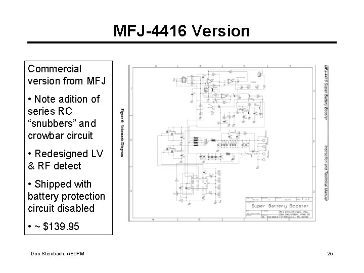
MFJ-4416 Version Commercial version from MFJ • Note adition of series RC “snubbers” and crowbar circuit • Redesigned LV & RF detect • Shipped with battery protection circuit disabled • ~ $139. 95 Don Steinbach, AE 6 PM 25
The End Mary Gomez Park Incident Solved Don Steinbach, AE 6 PM 26
- Slides: 26