Basics of Semiconductors By Saurav Thakur Btech EE
")
Basics of Semiconductors By Saurav Thakur (Btech EE)

Semiconductor Materials ● ● ● Semiconductors are of 2 types elemental and compounds semiconductors Elemental consists of just one element of group 4 while compound has a group 4 element and elements near metalloid staircase like group 5 or 3 or both are too present. The elemental is used for making transistors and diodes while compound a used in LEDs or even adding flexibility in the materials Doping is controlled addition of impurities in order to alter the conductivity and the charge carrier properties Energy band gap is difference of energy between conduction band valence band
 Miller Indices Calculating for a plane (0, 3, 0) x")
z (0, 0, 1) Miller Indices Calculating for a plane (0, 3, 0) x ● ● (2, 0, 0) y ● Find intercepts along axes – 2, 3, 1 ● Take reciprocal ● Convert to smallest integers in the same ratio – 3, 2 ● Enclose in parenthesis – (3, 2, 6) Equivalent planes are collectively represented in{h, k, l} like for a square {1, 0 For vectors their ratio of direction cosines are used to represent their Miller indices [h, k, l] like a diagonal of a square has [1, 0, 0]

Diamond Lattice ● ● ● Carbon atoms form fcc and fill all the tetrahedral voids in the lattice. The structure is also known as interpenetrating fcc It has inferior packing fraction (nearly 34%) as compared to fcc (74%) Zinc blende structure or Wurtzite structure has alternate tetrahedral voids occupied by zinc and sulphur makes fcc sublattice

Atomic Theory and Quantum Mechanics Photoelectric Effect � Atomic Spectra ● ● The emission of light due to transition of electron from higher energy orbit a lower energy orbital It is govern by the Bohr’s model of the atom which is based on existence o quantified energy states in the atom and hence the transition create the ligh wavelength corresponding to the energy difference of the orbitals

Bohr’s Model

Schrödinger Equation ● ● This is a partial differential equation that describes how the wavefunction o physical system evolves over time. Image source-csbsju. ed

Quantum Tunnelling ● ● Quantum tunnelling refers to the quantum mechanical phenomenon where particle tunnels through a barrier that it classically could not surmount In the figure the left side wave passes through the barrier which is of finite length but its amplitude is reduced ● As electrons are too wave so they can cross a finite barrier ● This phenomena is observed in nanoscale diodes and transistors ● This could be solved by Schrödinger equation thus obtaining terms of exponentials as the solutions Image source-wikimedia. o

Molecular Orbital Theory ● ● ● It is a method of representation and determining the structures of the molecular orbital formed when two atoms combine to form bond The method uses LCAO(linear combination of atomic orbitals) The atomic orbital combine to give bonding orbital(with lower energy) and antibonding orbital (with higher energy) Antibonding Orbital Atomic Orbitals Bonding Orbital

Band Theory ● ● ● For conduction the electrons must reach conduction band from valence ban The energy difference between the valence band conduction band is called band gap Insulators have a high band gap while conductors don’t have any but semiconductors have approx~1 e. V

● ● ● If the electron can reach the minimum energy required for conduction band from valence band without changing the momentum is called Direct Band If the electron has to change the momentum i. e. changing k(wave vector) to to minimum energy point is called Indirect Band Gap Direct band gap materials are used in LASERs
 Carrier generation")
Charge Carriers ● ● Holes Carry positive charge(equal to the electronic charge) Carrier generation and Recombination are processes by which mobile char carriers(electrons and holes) are created and eliminated(combining to relea energy) More abundant charge is called the Majority carrier while the other is calle the Minority carrier

Effective Mass

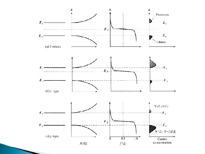
Carrier Concentration Fermi Level

Fermi Level ● ● ● Depending on the doping material the Fermi level tends to shift like for intrinsic semiconductor it is exactly in the center of the conduction and valence band For n type it shift towards conduction as electrons are in abundance so probability actually shifts towards conduction band On contrary for p type the shift is towards valence band or it could be said probability of holes =1 -probability of electrons at particular energy so hole show similar pattern as electrons show in n type semiconductor

Carrier Concentration

Conductivity and mobility

- Slides: 19