Basic Processor Structure ECE 352 Digital System Fundamentals
Basic Processor Structure ECE 352 Digital System Fundamentals Basic Processor Structure 1
Designing Computers 101 Basic Processor Structure • • • Defines instructions and their operands At a basic level, the computer architecture is divided into datapath and control • • • 2 Computer’s programming interface is called the instruction set architecture (ISA) Datapath defined by the set of registers, possible microoperations, and the control interface The control unit instructs the datapath to perform the needed computations The datapath may access information in memory in addition to its registers
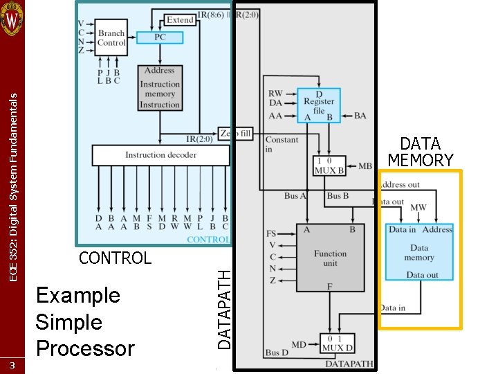
02 3 Example Simple Processor DATAPATH ECE 352: Digital System Fundamentals DATA MEMORY CONTROL
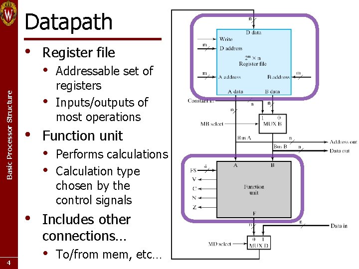
Datapath Basic Processor Structure • • • 4 Register file Addressable set of registers Inputs/outputs of most operations Function unit • • Performs calculations Calculation type chosen by the control signals Includes other connections… • To/from mem, etc…
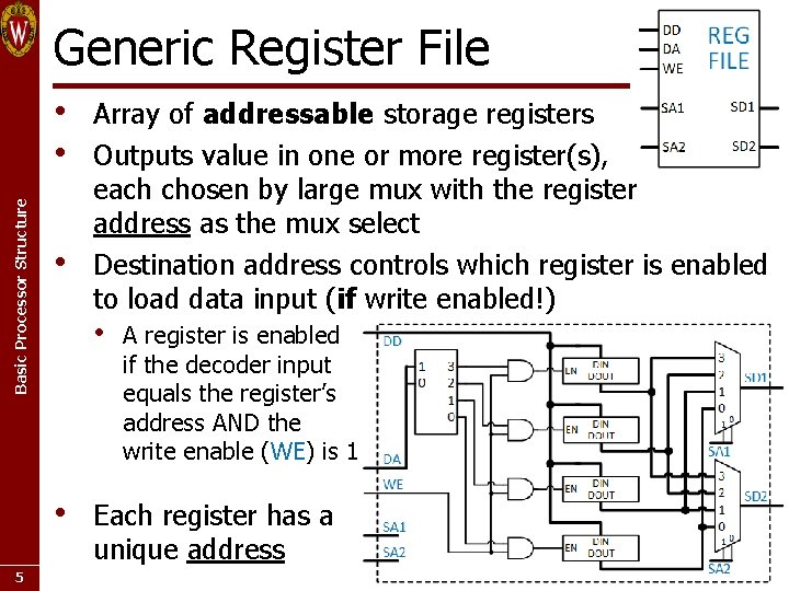
Generic Register File Basic Processor Structure • • • 5 Array of addressable storage registers Outputs value in one or more register(s), each chosen by large mux with the register address as the mux select Destination address controls which register is enabled to load data input (if write enabled!) A register is enabled if the decoder input equals the register’s address AND the write enable (WE) is 1 Each register has a unique address
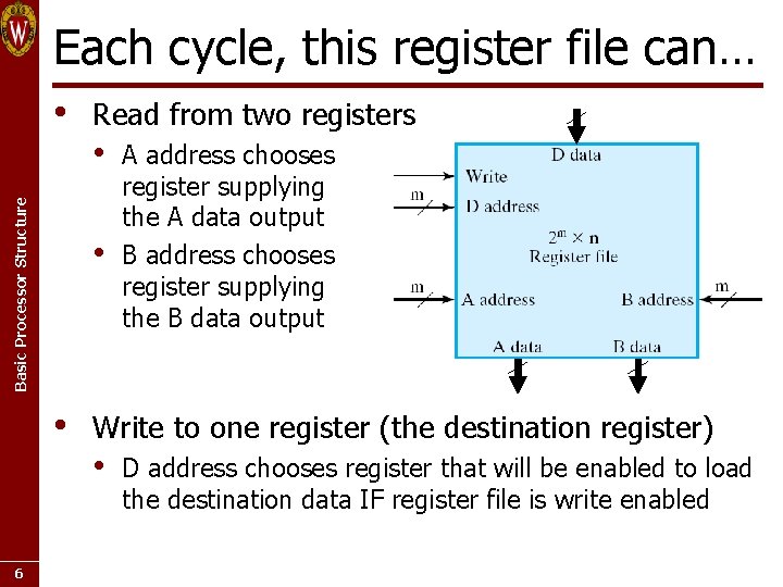
Each cycle, this register file can… Basic Processor Structure • • 6 Read from two registers A address chooses register supplying the A data output B address chooses register supplying the B data output Write to one register (the destination register) • D address chooses register that will be enabled to load the destination data IF register file is write enabled
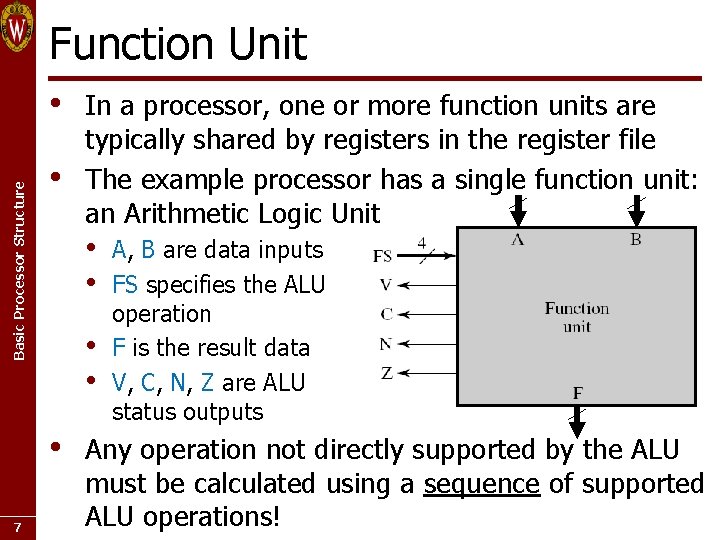
Function Unit Basic Processor Structure • • 7 In a processor, one or more function units are typically shared by registers in the register file The example processor has a single function unit: an Arithmetic Logic Unit A, B are data inputs FS specifies the ALU operation F is the result data V, C, N, Z are ALU status outputs Any operation not directly supported by the ALU must be calculated using a sequence of supported ALU operations!
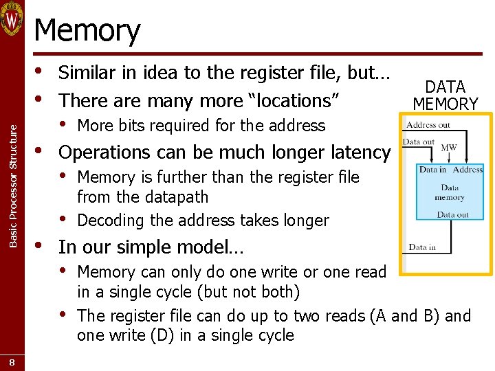
Memory Basic Processor Structure • • Similar in idea to the register file, but… There are many more “locations” • More bits required for the address Operations can be much longer latency • • Memory is further than the register file from the datapath Decoding the address takes longer In our simple model… • • 8 DATA MEMORY Memory can only do one write or one read in a single cycle (but not both) The register file can do up to two reads (A and B) and one write (D) in a single cycle
Datapath Operation Basic Processor Structure • The datapath completes a single microoperation during each clock cycle • • • The control unit must configure the datapath to make it perform the desired operation • • • 9 True for our processor… another advanced topic… Even when it is not true, that is usually hidden from the programmer Source operand location(s) • Register file, immediate data, and/or memory Destination location • Register file or memory Function unit operation (if used)
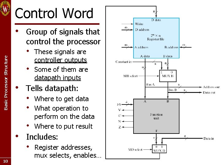
Control Word Basic Processor Structure • • • 10 Group of signals that control the processor These signals are controller outputs Some of them are datapath inputs Tells datapath: • • • Where to get data What operation to perform on the data Where to put result Includes: • Register addresses, mux selects, enables…
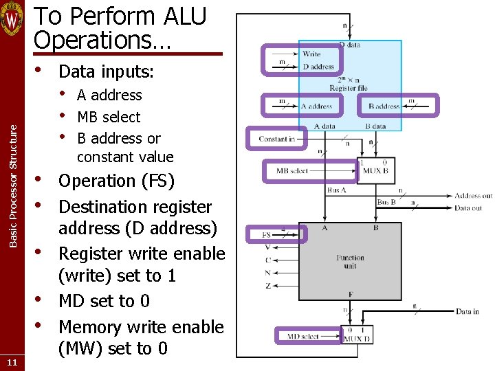
Basic Processor Structure To Perform ALU Operations… • Data inputs: • • 11 A address MB select B address or constant value Operation (FS) Destination register address (D address) Register write enable (write) set to 1 MD set to 0 Memory write enable (MW) set to 0
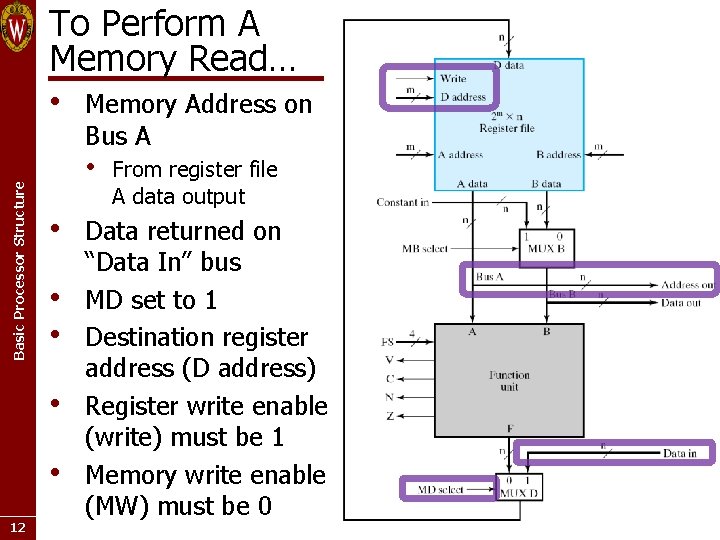
To Perform A Memory Read… • Memory Address on Basic Processor Structure Bus A • • • 12 From register file A data output Data returned on “Data In” bus MD set to 1 Destination register address (D address) Register write enable (write) must be 1 Memory write enable (MW) must be 0
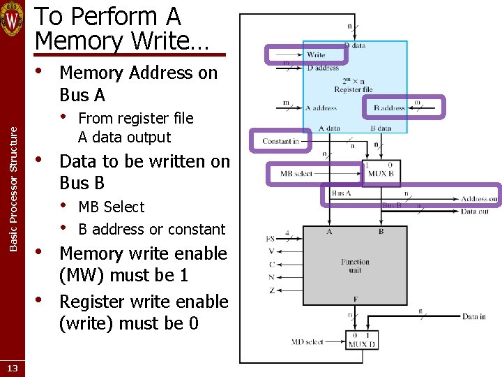
To Perform A Memory Write… • Memory Address on Basic Processor Structure Bus A • • 13 From register file A data output Data to be written on Bus B • • MB Select B address or constant Memory write enable (MW) must be 1 Register write enable (write) must be 0
Keep in mind… Basic Processor Structure • • • Even if certain control signal values are irrelevant for a given operation, some value must still be provided to the datapath • • Write enables should never be “don’t-care”… These examples are for this specific datapath… • • • 14 Signals should always have a valid value Just doesn’t matter whether they are 1 or 0 A different datapath may have different control signals in the control word! A different datapath may have active-low write enables! Need to look at the datapath, look at the connections, look at the muxes, read the specification…
Using the Datapath Basic Processor Structure • • • Figuring out what control signal values you need to give it for a required operation Figuring out how the datapath responds to a set of control signals • • 15 Making the datapath do what you need Looking at how the control signals affect multiplexers, write enables, where source information comes from Examples…
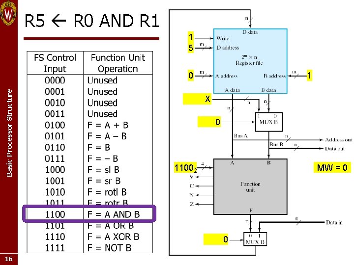
R 5 R 0 AND R 1 1 5 1 Basic Processor Structure 0 X 0 11002 MW = 0 0 16
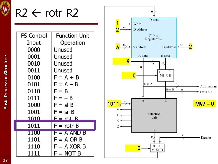
R 2 rotr R 2 1 2 2 Basic Processor Structure X X 0 10112 MW = 0 0 17
![R 7 mem[R 0] 1 7 X Basic Processor Structure 0 X X XXXX R 7 mem[R 0] 1 7 X Basic Processor Structure 0 X X XXXX](http://slidetodoc.com/presentation_image_h2/041a71d82d281d88ab40622a1be30a53/image-18.jpg)
R 7 mem[R 0] 1 7 X Basic Processor Structure 0 X X XXXX 2 MW = 0 1 18
![mem[R 4] R 6 0 X 6 Basic Processor Structure 4 X 0 XXXX mem[R 4] R 6 0 X 6 Basic Processor Structure 4 X 0 XXXX](http://slidetodoc.com/presentation_image_h2/041a71d82d281d88ab40622a1be30a53/image-19.jpg)
mem[R 4] R 6 0 X 6 Basic Processor Structure 4 X 0 XXXX 2 MW = 1 X 19
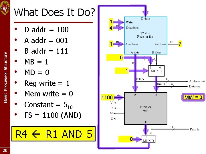
Basic Processor Structure What Does It Do? • • • D addr = 100 A addr = 001 B addr = 111 MB = 1 MD = 0 Reg write = 1 Mem write = 0 Constant = 510 FS = 1100 (AND) R 4 R 1 AND 5 20 1 4 7 1 5 1 11002 MW = 0 0
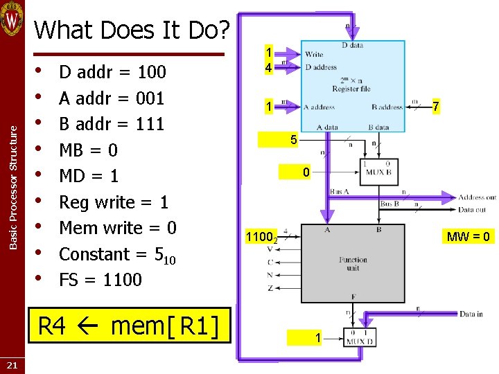
Basic Processor Structure What Does It Do? • • • D addr = 100 A addr = 001 B addr = 111 MB = 0 MD = 1 Reg write = 1 Mem write = 0 Constant = 510 FS = 1100 R 4 mem[ R 1] 21 1 4 7 1 5 0 11002 MW = 0 1
Basic Processor Structure ECE 352 Digital System Fundamentals Basic Processor Structure 22
- Slides: 22