Basic Principles of CCD Imaging in Astronomy Based

Basic Principles of CCD Imaging in Astronomy Based on Slides by Simon Tulloch available from http: //www. ing. iac. es/~smt/CCD_Primer. htm

What is a CCD? • “CCD” = “Charge-Coupled Device” • Invented in 1970 s, originally for: – Memory Devices – Arithmetic Processing of Data • When Made of Silicon (Si), has same Light. Sensitive Properties as Light Meters – Use them to “Measure” Light • Applied to Imaging as Sensor

CCDs in Astronomy • Revolutionized Astronomical Imaging – More Sensitive than Photographic Emulsions • Factor of 100 Measure Light only 0. 01 as Bright – Improved Light-Gathering Power of Telescopes by nearly 100 • Amateur w/ 15 -cm (6") Telescope + CCD can get similar performance as 1960 s Professional with 1 -m (40") Telescope + Photography • Now Considered to be “Standard” Sensor in Astronomical Imaging – Special Arrangements with Observatory Now Necessary to use Photographic Plates or Film
 •")
What is a CCD? • Made from Crystalline Material – Typically Silicon (Si) • CCD Converts “Light” to “Electronic Charge” – Spatial Pattern of Light Produces a Spatial Pattern of Charge = “Image” 1. “Digitized” – Analog Measurements (“Voltages”) Converted to Integer Values at Discrete Locations 2. Stored as Computer File

Si Crystal Structure • Regular Pattern of Si atoms – Fixed Separations Between Atoms • Atomic Structure Pattern “Perturbs” Electron Orbitals – Changes Layout of Available Electron States from Model of Bohr Atom http: //www. webelements. com/webelements/text/Si/xtal. html

Electron States in Si Crystal • Available States in Crystal Arranged in Discrete “Bands” of Energies – Lower Band Valence Band • More electrons – Upper Band Conduction Band • Fewer electrons • No States Exist in “Gap” Between Bands Increasing energy Conduction Band of Electron States “Gap” - - - Valence Band of Electron States “Gap” = 1. 12 electron-volts (e. V)

Comparison of State Structure in Crystal with Bohr Model Conduction Band Orbitals Valence Band “Gap” States “Blur” Together To Form “Bands” Discrete Transition Isolated Atom (as in Gas) Single Atom in Crystal

Action of Light on Electron States • Incoming Photon w/ Energy 1. 12 e. V Excites Electrons From “Valence Band” to “Conduction Band” • Electron in Conduction Band Moves in the Crystal “Lattice” • Excited Electron e- leaves “Hole” (Lack of Electron = h+) in Valence Band – Hole = “Carrier” of Positive Charge

Action of “Charge Carriers” • Carriers are “Free” to Move in the Band – Electron e- in Conduction Band – Hole h+ in Valence Band • Charge Carriers may be “Counted” – Measurement of Number of Absorbed Photons

Maximum to “Jump” Si Band Gap • 1 e. V = 1. 602 10 -12 erg = 1. 602 10 -12 Joule To Energize Electron in Si Lattice Requires < 1. 1 m

Energy and Wavelength • Incident Wavelength > 1. 1 m Photon CANNOT be Absorbed! – Insufficient Energy to “Kick” Electron to Conduction Band Silicon is “Transparent” to long CCDs constructed from Silicon are Not Sensitive to Long Wavelengths

After Electron is Excited into Conduction Band…. • Electron and Hole Usually “Recombine” Quickly – Charge Carriers are “Lost” • Apply External Electric Field to “Separate” Electrons from Holes • “Sweeps” Electrons Away from Holes – Maintains Population of “Free” Electrons – Allows Electrons to be “Counted”

pho n to pho ton Generation of CCD Carriers Conduction Band Hole Electron Valence Band

n to pho Conduction Band Valence Band pho ton Spontaneous Recombination

Prevent Spontaneous Recombination by Applying Voltage to “Sweep” Electrons + + + Ammeter

Prevent Spontaneous Recombination by Applying Voltage to “Sweep” Electrons + + + Ammeter

Thermal “Noise” • Big BUT: Other Kinds of Energy Have Identical Effect • Thermally Generated Electrons are Indistinguishable from Photon-Generated Electrons – Heat Energy can “Kick” e- into Conduction Band – Thermal Electrons appear as “Noise” in Images • “Dark Current” – Keep CCDs COLD to Reduce Number of Thermally Generated Carriers (Dark Current)
? • Must “Move” Charges to an “Amplifier”")
How Do We “Count” Charge Carriers (“Photoelectrons”)? • Must “Move” Charges to an “Amplifier” • Astronomical CCDs: Amplifier Located at “Edge” of Light-Sensitive Region of CCD – Charge Transfer is “Slow” – Most of CCD Area “Sensitive” to Light • Video and Amateur Camera CCDs: Must Transfer Charge QUICKLY – Less Area Available to Collect Light

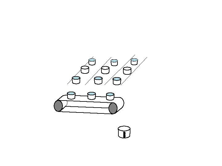
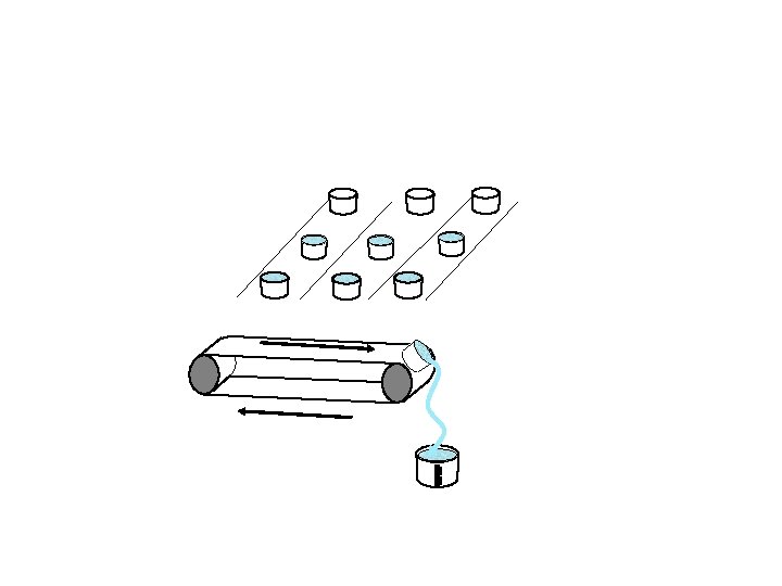
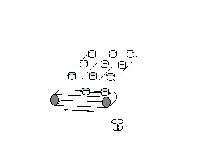
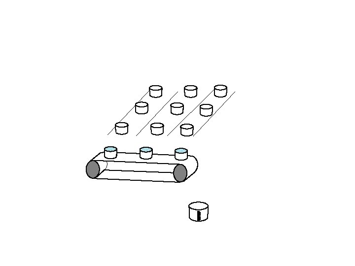
“Bucket Brigade” CCD Analogy • Electron Charge Generated by Photons is “Transferred” from Pixel to “Edge” of Array • Transferred Charges are “Counted” to Measure Number of Photons
 CONVEYOR BELT (SERIAL REGISTER) VERTICAL COLUMNS of PIXELS MEASURING")
Rain of Photons BUCKETS (PIXELS) CONVEYOR BELT (SERIAL REGISTER) VERTICAL COLUMNS of PIXELS MEASURING CYLINDER (OUTPUT AMPLIFIER)

Rain of Photons Shutter
")
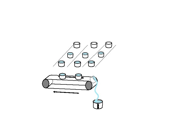
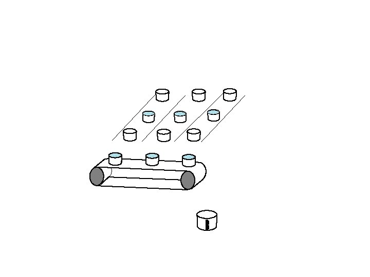
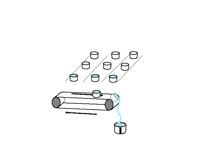
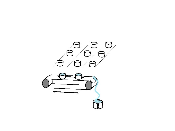
Empty First Buckets in Column Into Buckets in Conveyor Belt CONVEYOR BELT (SERIAL REGISTER) MEASURING CYLINDER (OUTPUT AMPLIFIER)
 MEASURING CYLINDER (OUTPUT AMPLIFIER)")
CONVEYOR BELT (SERIAL REGISTER) MEASURING CYLINDER (OUTPUT AMPLIFIER)

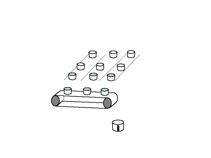
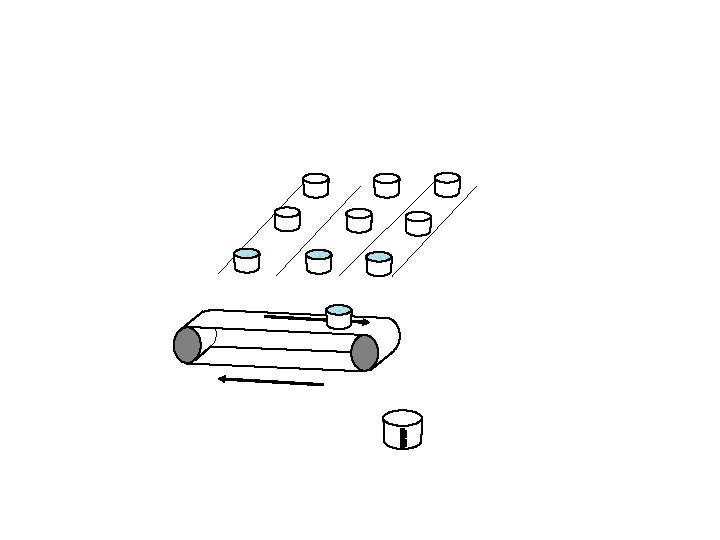
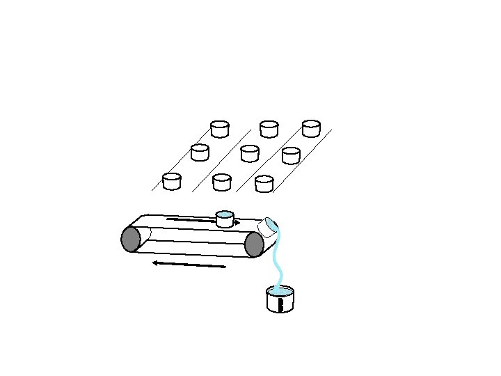
Empty Second Buckets in Column Into First Buckets

Empty Third Buckets in Column Into Second Buckets

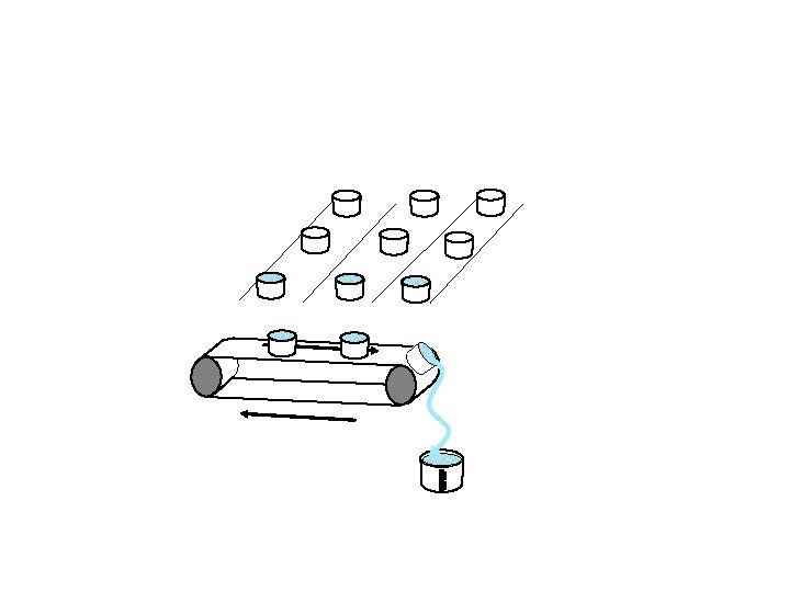
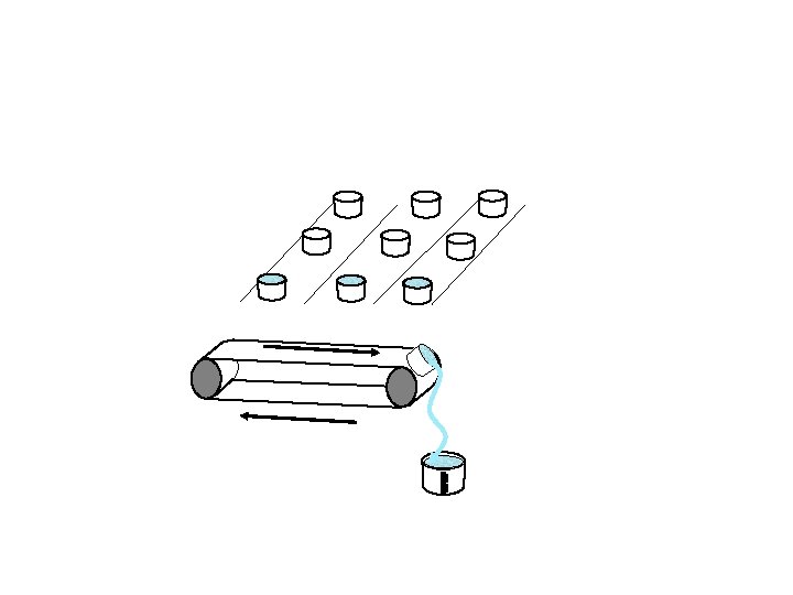
Start Conveyor Belt

After each bucket has been measured, the measuring cylinder is emptied, ready for the next bucket load. Measure & Drain
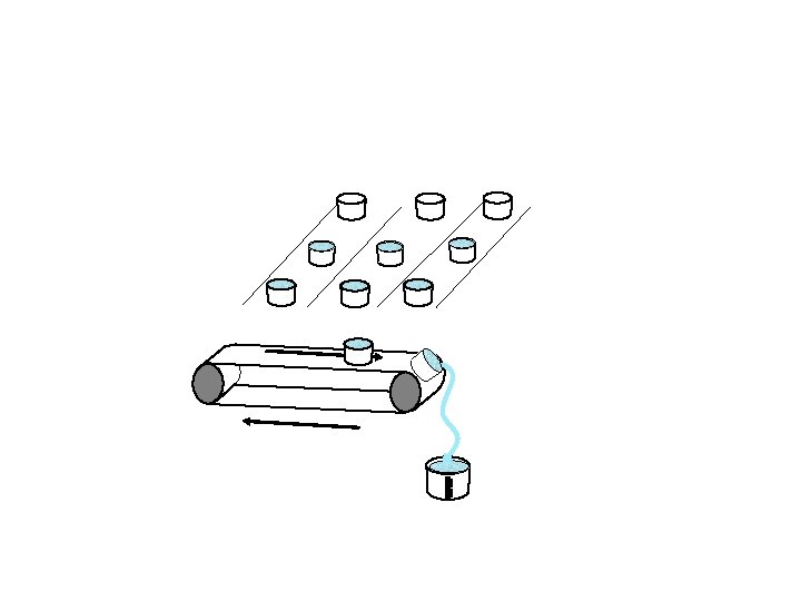

Measure & Drain
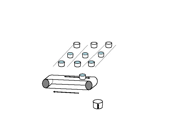

Empty First Buckets in Column Into Buckets in Conveyor Belt Now Empty

Empty Second Buckets in Column Into First Buckets

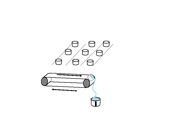
Start Conveyor Belt

Measure & Drain

Measure & Drain

Measure & Drain

Empty First Buckets in Column Into Buckets in Conveyor Belt

Start Conveyor Belt

Measure & Drain

Measure & Drain

Measure & Drain

Ready for New Exposure

Features of CCD Readout • Pixels are Counted in Sequence – Number of Electrons in One Pixel Measured at One Time – Takes a While to Read Entire Array • Condition of an Individual Pixel Affects Measurements of ALL Following Pixels – A “Leaky” Bucket Affects Other Measurements in Same Column
 for this Pixel AND following Pixel Less Charge Measured")
“Leaky” Bucket Loses Water (Charge) for this Pixel AND following Pixel Less Charge Measured for This Column
 • Image Area")
Structure of Astronomical CCDs Image Area Package Serial register (Conveyor Belt) • Image Area of Connection pins CCD Located at Focal Plane of Gold bond wires Telescope Bond pads • Image Builds Up During Exposure • Image Transferred, Silicon chip pixel-by-pixel to Output amplifier Output Amplifier

CCD Manufacture Don Groom LBNL
")
Fabricated CCD Kodak KAF 1401 1317 1035 pixels (1, 363, 095 pixels)

Charges (“Buckets” are Moved by Changing Voltage Pattern Apply Voltages Here 1 2 3

Charge Transfer 1 2 3

Charge Transfer - 1 +5 V 2 0 V -5 V +5 V 1 2 3 1 0 V -5 V +5 V 3 0 V -5 V Time-slice shown in diagram

Charge Transfer - 2 +5 V 2 0 V -5 V +5 V 1 2 3 1 0 V -5 V +5 V 3 0 V -5 V

Charge Transfer - 3 +5 V 2 0 V -5 V +5 V 1 2 3 1 0 V -5 V +5 V 3 0 V -5 V

Charge Transfer - 4 +5 V 2 0 V -5 V +5 V 1 2 3 1 0 V -5 V +5 V 3 0 V -5 V

Charge Transfer - 5 +5 V 2 0 V -5 V +5 V 1 2 3 1 0 V -5 V +5 V 3 0 V -5 V

Charge Transfer - 6 +5 V 2 0 V -5 V +5 V 1 2 3 1 0 V -5 V +5 V 3 0 V -5 V

Charge Transfer - 7 +5 V 2 0 V -5 V +5 V 1 2 3 1 0 V -5 V +5 V 3 0 V -5 V

CCD “Blooming” - 1 Charge Capacity of CCD pixel is Finite (Up to 300, 000 Electrons) After Pixel Fills, Charge Leaks into adjacent pixels. Spillage pixel boundary Photons pixel boundary Overflowing charge packet Photons Spillage
 Charge Transfer Direction Charge Spreads in")
CCD “Blooming” - 2 Channel “Stops” (Charge Barrier) Charge Transfer Direction Charge Spreads in Column • Up AND Down Flow of bloomed charge

CCD “Blooming” - 3 M 42 • Long Exposure for Faint Nebulosity Star Images are Overexposed Bloomed Star Images with “Streaks”

CCD Image Defects • “Dark” Columns – Charge “Traps” Block Charge Transfer – “Charge Bucket” with a VERY LARGE Leak • Not Much of a Problem in Astronomy – 7 Bad Columns out of 2048 Little Loss of Data

CCD Image Defects 1. Bright Columns Bright Column – 2. Hot Spots – Cluster of Hot Spots Electron “Traps” – Pixels with Larger Dark Current Caused by Fabrication Problems 3. Cosmic Rays ( ) Cosmic rays – – – Unavoidable Ionization of e- in Si Can Damage CCD if High Energy (HST)

CCD Image Defects M 51 Negative Image Dark Column Hot Spots, Bright Columns Bright First Row • incorrect operation of signal processing electronics

CCD Image Processing • • “Raw” CCD Image Must Be Processed to Correct for Image Errors CCD Image is Combination of 4 Images: 1. 2. 3. 4. “Raw” Image of Scene “Bias” Image “Dark Field” Image with Shutter Closed “Flat Field” Image of Uniformly Lit Scene

Bias Frame • Exposure of Zero Duration with Shutter Closed – “Zero Point” or “Baseline” Signal from CCD – Resulting Structure in Image from Image Defects and/or Electronic “Noise” • Record 5 Bias Frames Before Observing – Calculate Average to Reduce Camera Readout Noise by 1/ 5 45%

“Dark Field” Image • Dark Current Minimized by Cooling • Effect of Dark Current is “Compensated” Using Exposures of Same Duration Taken with Shutter Closed. • Dark Frames are Subtracted from Raw Frames Dark Frame

“Flat Field” Image • Sensitivity to Light Varies from Pixel to Pixel – Fabrication Problems – Dust Spots – Lens Vignetting –… • Image of “Uniform” (“Flat”) Field – Twilight Sky at High Magnification – Inside of Closed Dome

Correction of Raw Image with Bias, Dark, Flat Images Raw File Dark Frame “Raw” “Dark” “Flat” “Bias” Flat Field Image Bias Image Output Image “Flat” “Bias”

Correction of Raw Image w/ Flat Image, w/o Dark Image Assumes Small Dark Current (Cooled Camera) Raw File Bias Image “Raw” “Bias” “Flat” “Bias” Output Image Flat Field Image “Flat” “Bias”
- Slides: 82