Basic of MicroElectromechanical System MEMS and Nano Electromechanical
 and Nano. Electromechanical System (NEMS)")
Basic of Micro-Electromechanical System (MEMS) and Nano. Electromechanical System (NEMS)

Outline • Microsystem product –MEMS • How to fabricate microsystem product – micro machining @ microfabrication

Microsystem

Microsystem products • Designing products that are smaller and are comprised of smaller components and sub- assemblies means less material usage, lower power requirements, greater functionality per unit space, and accessibility to regions that are forbidden to larger products. • Microsystem products can be classified by type of device (e. g. , sensor, actuator) or by application area (e. g. , medical, automotive).

Benefits from Microsystems • Miniaturization: save materials, save power, faster time response, better performance. • Integration: integrated with IC and other systems, reduce system size and cost; save adapters and interconnections. • Batch fabrication: cheap, disposable (most important driving force)

Microsensors • Micro sensors—A sensor is a device that detects or measures some physical phenomenon such as heat or pressure. It includes a transducer that converts one form of physical variable into another form (e. g. , a piezoelectric device converts mechanical force into electrical current) plus the physical packaging and external connections. • Most micro sensors are fabricated on a silicon substrate using the same processing technologies as those used for integrated circuits. • Microscopic-sized sensors have been developed for measuring force, pressure, position, speed, acceleration, temperature, flow, and a variety of optical, chemical, environmental, and biological variables. • The term hybrid micro sensor is often used when the sensing element (transducer) is combined with electronics components in the same device

Microactuators • Microactuators—Like a sensor, an actuator converts a physical variable of one type into another type, but the converted variable usually involves some mechanical action (e. g. , a piezoelectric device oscillating in response to an alternating electrical field). • An actuator causes a change in position or the application of force. Examples of microactuators include valves, positioners, switches, pumps, and rotational and linear motors.

Microstructures and microcomponents • Microstructures and micro components— These terms are used to denote a micro- sized part that is not a sensor or actuator. • Examples of microstructures and micro- components include microscopic lenses, mirrors, nozzles, and beams. • These items must be combined with other components (microscopic or otherwise) in order to provide a useful function.

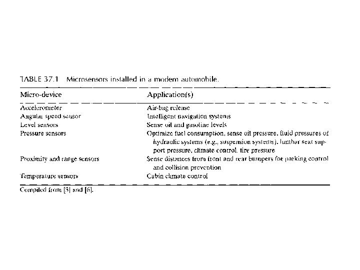
Microsensors and other microdevices • Automotive microsensors and other microdevices are widely used in modern auto- motive products. Use of these microsystems is consistent with the increased application of on-board electronics to accomplish control and safety functions for the vehicle. • The functions include electronic engine control, cruise control, anti-lock braking systems, air-bag deployment, automatic transmission control, power steering, all-wheel drive, automatic stability control, on-board navigation systems, and remote locking and unlocking, not to mention air conditioning and radio. • These control systems and safety features require sensors and actuators, and a growing number of these are microscopic in size. There are currently 20 to 100 sensors installed in a modern automobile, depending on make and model.
 • Electronics—Printed circuit board (PCB) and connector technologies also be")
Electronics—Printed circuit board (PCB) • Electronics—Printed circuit board (PCB) and connector technologies also be cited here in the context of micro system technology (MST). • Miniaturization trends in electronics have forced PCBs, contacts, and connectors to be fabricated with smaller and more complex physical details, and with mechanical structures that are more consistent with the microdevices with the integrated circuits. • Compact Discs (CDs) represent important commercial products to day, as storage media for audio, video, and computer software storage applications. CDs are massproduced by plastic molding of polycarbonate. The molds for the process are fabricated using microsystem technology.
")
MICROELECTRO MECHANICAL SYSTEMS (MEMS)

MEMS • What are MEMS? Ø • Micro - Small size, microfabricated structures • Electro - Electrical signal /control ( In / Out ) • Mechanical - Mechanical functionality (Out/ In ) • Systems - Structures, Devices, Systems controls • What is the size of MEMS? • MEMS are made up of components between 1 to 100 micrometers in size • MEMS devices generally range in size from 20 micrometers to a millimeter
 • MEMS is a technology of very small devices. It")
MICROELECTRO MECHANICAL SYSTEMS (MEMS) • MEMS is a technology of very small devices. It is a combination of mechanical functions and electrical functions on the same chip using micro fabrication technology. • MEMS emphasizes the miniaturization of systems consisting of both electronic and mechanical components. The word MICROMACHINES is sometimes used for these systems. • MEMS are rarer, but typical examples are airbag sensors and digital micromirror devices • Microsystem technology (MST) is a more general term that refers to the products (not necessarily limited to electromechanical products) as well as the fabrication technologies used to produce them.

• A related term is Nanotechnology, which refers to even smaller devices whose dimensions are measured in nanometers (10 -9 m). • Examples of such systems are electromagnetic microactuators for rigid disk drives, microgimbals, microbellows, and various probes, sensors, and measuring devices. • Micromachining operations for manufacturing these components usually involve chemical etching processes on a very fine scale. • One area of interest for microelectromechanical systems is their use as probes and measuring devices, including aerospace and fluid-flow applications. Especially of interest is their incorporation into fiber-optic systems.

Micro mirror device

How MEMS are prepared? There are three basic processes of fabrication in MEMS technology. 1. Deposition: The ability to deposit thin films of material on a substrate. 2. Lithography: To apply a patterned mask on top of the films by photolithograpic imaging. 3. Etching: To etch the films selectively to the mask. 3/4/2021 18

General Fabrication of MEMS Deposition Patterning Etching Physical Chemical Lithography Dry Wet Photolithography Electron beam lithography Ion track technology X-ray lithography.

1. Deposition MEMS deposition technology can be classified in two groups: 1. Depositions that happen because of a chemical reaction: • • 2. Depositions that happen because of a physical reaction: • • 3/4/2021 Chemical Vapor Deposition (CVD) Electrodeposition Epitaxy Thermal oxidation Physical Vapor Deposition (PVD) Casting 20

2. Lithography MEMS lithography technology can be classified in two groups: 1. Pattern Transfer 2. Lithographic Module a. b. c. d. e. 3/4/2021 Dehydration bake and HMDS prime Resist spin/spray and Soft bake Alignment, Exposure Post exposure bake and Hard bake Descum 21

3. Etching There are two classes of etching process: 1. Wet etching: The material is dissolved when immersed in a chemical solution. 2. Dry etching: The material is sputtered or dissolved using reactive ions or a vapor phase etchant. 3/4/2021 22

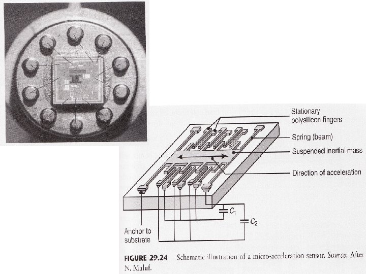
MEMS Applications 1. 2. 3. 4. 5. 6. 7. 8. Micro-engines –Micro Reactors, Vibrating Wheel Inertial Sensors –Virtual Reality Systems Accelerometers –Airbag Accelerometer Pressure Sensors –Air Pressure Sensors Optical MEMS –Pill Camera Fluidic MEMS -Cartridges for Printers Bio MEMS -Blood Pressure Sensors MEMS Memory Units -Flash Memory 3/4/2021 23

i. Phone: Techno Sensitiveness • The two key elements of MEMS are: 1. MEMS sensor, the silicon mechanical element which senses the motion; 2. Interface chip, the IC which converts the motion measured by the sensor into an analog or digital signal. 3/4/2021 24

Bio MEMS Application An implantable blood pressure sensor developed by Cardio. MEMS 3/4/2021 25

MEMS Advantages 1. Minimize energy and materials use in manufacturing 2. Cost/performance advantages 3. Improved reproducibility 4. Improved accuracy and reliability 5. Increased selectivity and sensitivity 3/4/2021 26

MEMS Disadvantages 1. Farm establishment requires huge investments 2. Micro-components are Costly compare to macro-components 3. Design includes very much complex procedures 4. Prior knowledge is needed to integrate MEMS devices 3/4/2021 27

Micromachining @ microfabrication

Figure: Micro Machining Definition: material removal at micro level with no constraint on the size of the component being machined. Removal of material in the form of chips having the size in the range of microns.

Why Micro Machining? Present day High-tech Industries, Design requirements are stringent. – Extraordinary Properties of Materials (High Strength, High heat Resistant, High hardness, Corrosion resistant etc. ) – Complex 3 D Components (Turbine Blades) – Miniature Features (filters for food processing and textile industries having few tens of microns as hole diameter and thousands in number) – Nano level surface finish on Complex geometries (thousands of turbulated cooling holes in a turbine blade) – Making and finishing of micro fluidic channels (in electrically conducting & non conducting materials, say glass, quartz, &ceramics)
 process")
Micromachining techniques 1. Bulk Micro-machining 2. Surface Micro-machining 3. LIGA (Lithographic, electrodeposition, molding) process 4. Silicon layer processes

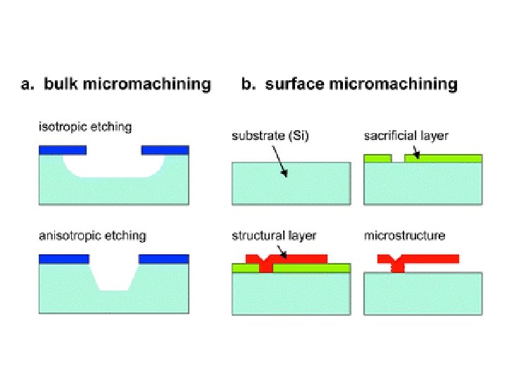
1. Bulk micromachining • Bulk and surface micromachining are processes used to create microstructures on microelectromechanical MEMS devices. • While both wet and dry etching techniques are available to both bulk and surface micromachining, bulk micromachining typically uses wet etching techniques while surface micromachining primarily uses dry etching techniques. • Bulk micromachining selectively etches the silicon substrate to create microstructures on MEMS devices.
 Anisotropic etchants, (b) Isotropic etchants, (c) Reactive Ion Etching (RIE)")
Etched grooves using (a) Anisotropic etchants, (b) Isotropic etchants, (c) Reactive Ion Etching (RIE)
 is selectively")
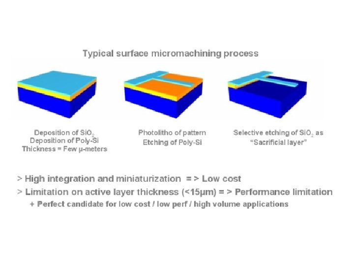
2. Surface micromachining • Unlike Bulk micromachining, where a silicon substrate (wafer) is selectively etched to produce structures, surface micromachining builds microstructures by deposition and etching of different structural layers on top of the substrate • Generally polysilicon is commonly used as one of the layers and silicon dioxide is used as a sacrificial layer which is removed or etched out to create the necessary void in the thickness direction • The main advantage of this machining process is the possibility of realizing monolithic microsystems in which the electronic and the mechanical components(functions) are built in on the same substrate.
 Spacer layer deposition. (b) Pattering of the spacer layer. (c) Deposition of the")
(a) Spacer layer deposition. (b) Pattering of the spacer layer. (c) Deposition of the microstructure layer. (d) Patterning of desired structure. (e) Stripping of the spacer layer resolves final structure.

3. LIGA is a process that can make complex microstructures with very high aspect ratios. It can make structures that are composed of electroplated metals or of injected plastics using the LIGA-fabricated structures as molds. The word LIGA comes from the German words: a) Lithographie—lithography, typically x-ray lithography b) Galvanoformung—electroplating of a suitable metal into high aspect ratio resist structures c) Abformung—molding of other materials into the high aspect ratio structures The letters also indicate the LIGA process sequence

Using LIGA, structures with thicknesses up to several millimeters with small lateral dimensions. The LIGA process can build microparts that are smaller than conventional machining processes and also bigger than surface micromachined parts. In this manner it fills a gap in the size range of microparts. It is also capable of parallel processing, meaning that it can be designed to be a manufacturable process.

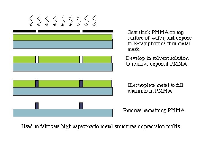
LIGA process 1. 2. 3. 4. Apply resist, X-ray exposure through mask, Remove exposed portions of resist, Electrode position to fill openings in resist, Strip resist for (a) mold or (b) metal part

Detail processes of LIGA 1. Apply resist, X-ray exposure through mask A thick layer of (X-ray) radiation –sensitive resist is applied to a substrate. The common resist material used in LIGA is polymethylmethacrylite (PMMA). The substrate must be a conductive material for subsequent electrodeposition process performed. The resist is exposed through a mask to high energy X-ray radiation. 2. Remove exposed portions of resist The irradiated areas of the positive resist are chemically removed from the substrate surface, leaving the unexposed portions standing as a 3 D plastic structure.

Detail processes of LIGA 3. Electrode position to fill openings in resist The regions where the resist has been removed are filled with metal using electrodeposition. Nickel are common plating metal used in LIGA. 4. Strip resist for (a) mold or (b) metal part The remaining resist structure is stripped (removed), yielding a 3 D metal structure. Depending on the geometry created, this metallic structure may be: a) the mold used for producing plastic parts by injection molding or compression molding. In case of injection molding, in which thermoplastic parts are produced. b) the metal part may be a pattern for fabricating plastic molds that will be used to produce more metallic parts by electodeposition.

An illustration of the steps involved in the LIGA process to fabricate high aspect ratio MEMS devices

Advantages in LIGA 1. LIGA is a versatile process – it can produce parts by several different methods 2. High aspect ratios are possible (large heightto-width ratios in the fabricated part) 3. Wide range of part sizes is feasible - heights ranging from micrometers to centimeters 4. Close tolerances are possible

Disadvantages in LIGA 1. LIGA is a very expensive process - Large quantities of parts are usually required to justify its application 2. LIGA uses X-ray exposure - Human health hazard

Microparts Fabricated by LIGA A major issue that remains for LIGA fabrication is the assembly of the microparts after fabrication is complete. The micro-parts must be manipulated into their correct positions to build the device. Microgears for micromachine applications High aspect ratio stator for a micromotor device

LIGA-fabricated fixture for optical fiber

4. Silicon layer processes Silicon is now widely used in Microsystem Technology to produce sensors, actuators, and other microdevices. The basic processing technologies are those used to produce integrated circuits (IC). Why silicon? 1. The microdevices often includes electronic circuits, so both the circuit and the microdevice can be fabricated in combination on the same substrate. 2. Silicon also possesses useful mechanical properties such as high strength and elasticity, good hardness and relatively low density. 3. The technology for processing silicon are well established, owing to their widespread use in microelectronics 4. Use of single crystal silicon permits the production of physical features to very close tolerances.

IC Fabrication Process Steps 1. Lithography: The process for pattern definition by applying thin uniform layer of viscous liquid (photo-resist) on the wafer surface. The photo-resist is hardened by baking and than selectively removed by projection of light through a reticle containing mask information. 2. Etching: Selectively removing unwanted material from the surface of the wafer. The pattern of the photo-resist is transferred to the wafer by means of etching agents. 3. Deposition: Films of the various materials are applied on the wafer. For this purpose mostly two kind of processes are used, physical vapor deposition (PVD) and chemical vapor deposition (CVD).

IC Fabrication Process Steps 4. Chemical Mechanical Polishing: A planarization technique by applying a chemical slurry with etchant agents to the wafer surface. 5. Oxidation: In the oxidation process oxygen (dry oxidation) or HO (wet oxidation) molecules convert silicon layers on top of the wafer to silicon dioxide. 6. Ion Implantation: Most widely used technique to introduce dopant impurities into semiconductor. The ionized particles are accelerated through an electrical field and targeted at the semiconductor wafer. 7. Diffusion: A diffusion step following ion implantation is used to anneal bombardment-induced lattice defects.

IC fabrication vs microfabrication It should be noted that certain differences exist between the processing of ICs and fabrication of the microdevices. The differences are: 1. The aspect ratios in microfabrication (LIGA etc) are generally much greater than in IC fabrication (silicon layer). Aspect ratio is defined as the height to width ratio of the features produced. Typical aspect ratios in semiconductor processing are about 1. 0 or less, whereas in microfabrication the corresponding ratio might be as high as 400. 2. The sizes of the devices made in microfabrication are often much larger than in IC processing, where the prevailing trend in microelectronics is inexorably towards greater circuit densities and miniaturization. 3. The structure produced in microfabrication often include cantilevers and bridges and other shape requiring gaps between layers. These kinds of structure are uncommon in IC fabrication. 4. The silicon processing techniques are sometimes supplemented to obtain a 3 D structure or other physical feature in the microsystem.
 typical in (a) fabrication of integrated circuits (b) micro fabricated")
Aspect ratio (height-to-width ratio) typical in (a) fabrication of integrated circuits (b) micro fabricated components.

The trend in miniaturization is expected to continue beyond microsystem technology. Nano technology

NANOTECHNOLOGY • Nanotechnology is the term used for the next generation of even smaller devices and their fabrication processes, which involve the control of feature sizes measured on the nanometer (one nm = 10 -9 m) scale. • Nanostructures consist of physical features whose dimensions are in the range 1 to 100 nm. Structures of this size can almost be thought of as purposely arranged collections of individual atoms and molecules. • Two alternative processing technologies will be used to fabricate items of this size: (1) additive molecular processes that build the nanostructure from individual atoms, and (2) nanofabrication technologies similar to microfabrication processes only performed on a smaller scale.

Nanofabrication Technologies • Nanofabrication processes are similar to those used in the fabrication of integrated circuits and microsystems, but they are carried out on a scale that is several orders of magnitude smaller than in microfabrication. • The processes involve the addition, alteration, and subtraction of thin layers using lithography to determine the shapes in the layers produced. • One significant difference is the lithography technologies that must be used at the smaller scales in nanofabrication.

• Ultraviolet photolithography cannot be used effectively, owing to the relatively long wavelengths of UV radiation. Instead, the preferred technique is high-resolution electron-beam lithography whose shorter wavelength virtually eliminates diffraction during exposure. • Another process emphasized in nanofabrication is molecular beam epitaxy, a layer addition technology, molecular-beam epitaxy (MBE) involves the growth of a single-crystal layer onto an existing crystalline substrate, so that the lattice of the new layer duplicates that of the existing substrate. Physical vapor deposition (PVD)is the process used to accomplish molecular beam epitaxy. • Nanofabrication techniques have already found applications in transistors for satellite microwave receivers, lasers used in communications systems, and compact disc players.
 (b) Figure (a) A scanning electron microscope view of a diamond-tipped (triangular")
Nanofabrication (a) (b) Figure (a) A scanning electron microscope view of a diamond-tipped (triangular piece at the right) cantilever used with the atomic force microscope. The diamond tip is attached to the end of the cantilever with an adhesive. (b) Scratches produced on a surface by the diamond tip under different forces. Note the extremely small size of the scratches.

Potential Applications • Nanofabrication has the potential to revolutionize many industries, including information storage, integrated circuit manufacture, and medical drug delivery systems. • For example, it has been estimated that if a bit of information could be stored in 100 atoms, then all of the books ever written could be stored in a 0. 5 -mm cube. • Scientists have envisioned the days when microscopic robots will be injected into the body and deliver drugs exactly where needed.

Terminology and relative sizes for microsystems and related technologies

Lecture highlights • MEMS: Definition, general fabrication, applications, advantages, disadvantages • Sequences of Micromachining @ microfabrication techniques - silicon layer process, LIGA • IC fabrication • Nanofabrication
- Slides: 61