Basic of logic design Sequential logic Quick Review

Basic of logic design Sequential logic

Quick Review • Combinational Logic • Encoder/Decoder • Mux/Demux • ALU • Sequential Logic • Memory! • Clock

Not your grandfather’s clock • Clock – “a free-running signal with a fixed cycle time” • Concretely: A crystal that vibrates when electric current is applied to it Abstractly: 3

Why clocks? “Electricity travels a foot in a nanosecond. ” Grace Murray Hopper Problem: Don’t want to update SE 2 before inputs are ready. Solution: Wait for a set amount of time (clock period). 4

Cross-Coupled Inverters

S-R Latch • Can have memory elements without clocks… • S- set • R - reset S R Q S-R latch Q’ 0 0 Q Q’ 0 1 0 1 1 0* 0* • … but usually one of the inputs is a clock. 6

D Latch Stores D when the clock is asserted C D Q Q’ 0 0 Q Q’ 0 1 1 7

Latch Behavior Data input Clock input Output 8

Implementation of a D flip-flop Master Slave Falling edge-triggered – Each latch is like a door. Input can pass through to output whenever the door is open. A flip-flop is like double doors. Data input Clock input Output 9

Use D Flip-flops to Create a Register D 0 D Q 0 C D 1 D DI Q 1 C C D 2 D Q 2 C D 3 D C Clk 4 4 Q 3 Clk DO

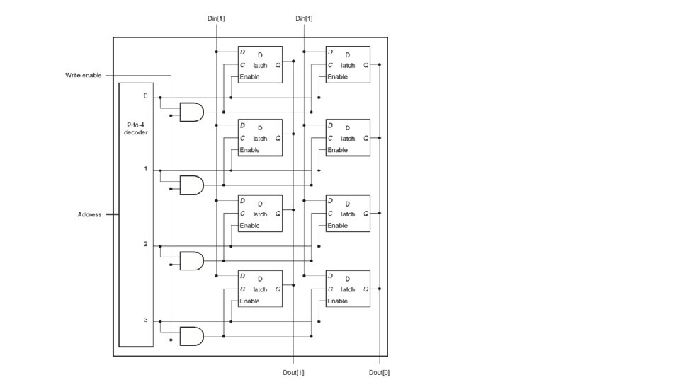
Register File

Read ports

Write ports

Memory elements: SRAM • Read: • Chip select – 1 • Output enable – 1 • Write • Chip select – 1 • Write enable - 1 • Output enable: • Connect multiple memories to the same bus
- Slides: 15