Basic MIPS Architecture SingleCycle Datapath and Control Chapter
Basic MIPS Architecture: Single-Cycle Datapath and Control Chapter 4 Sections 4. 1 – 4. 4 Appendix D. 1 and D. 2 Dr. Iyad F. Jafar
Outline �Introduction �Clocking �Single-cycle Datapath �Single-cycle Control �Performance Analysis 2
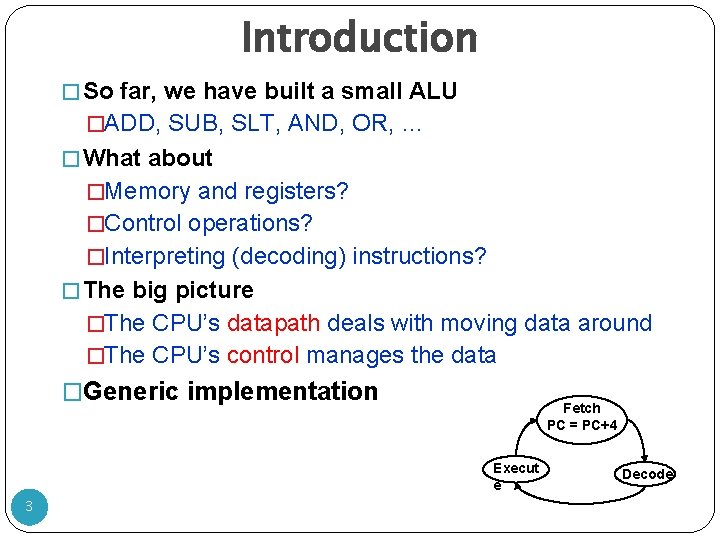
Introduction � So far, we have built a small ALU �ADD, SUB, SLT, AND, OR, … � What about �Memory and registers? �Control operations? �Interpreting (decoding) instructions? � The big picture �The CPU’s datapath deals with moving data around �The CPU’s control manages the data �Generic implementation Fetch PC = PC+4 Execut e 3 Decode
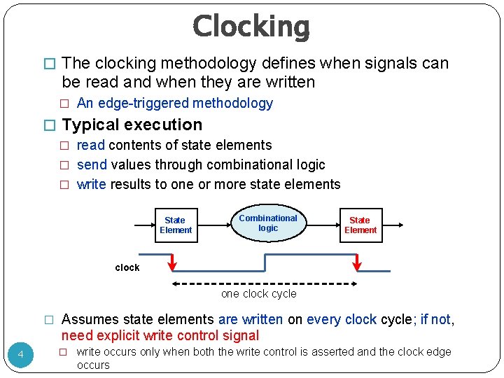
Clocking � The clocking methodology defines when signals can be read and when they are written � An edge-triggered methodology � Typical execution � read contents of state elements � send values through combinational logic � write results to one or more state elements State Element Combinational logic State Element clock one clock cycle � Assumes state elements are written on every clock cycle; if not, need explicit write control signal 4 � write occurs only when both the write control is asserted and the clock edge occurs
Single-Cycle Datapath �The first implementation considered �All instructions start and finish execution in one cycle! �This include the time required to fetch, decode, and execute the instruction �In the following, we will consider the datapath of each of these steps 5
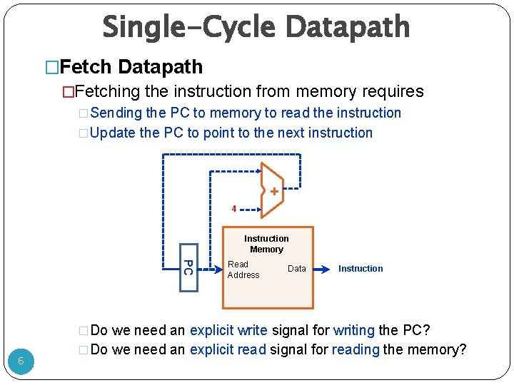
Single-Cycle Datapath �Fetching the instruction from memory requires �Sending the PC to memory to read the instruction �Update the PC to point to the next instruction + 4 Instruction Memory PC Read Address Data Instruction �Do we need an explicit write signal for writing the PC? 6 �Do we need an explicit read signal for reading the memory?
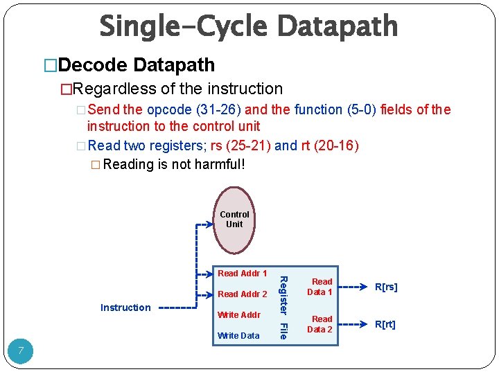
Single-Cycle Datapath �Decode Datapath �Regardless of the instruction �Send the opcode (31 -26) and the function (5 -0) fields of the instruction to the control unit �Read two registers; rs (25 -21) and rt (20 -16) � Reading is not harmful! Control Unit Read Addr 2 Instruction Write Addr Write Data 7 Register File Read Addr 1 Read Data 1 R[rs] Read Data 2 R[rt]
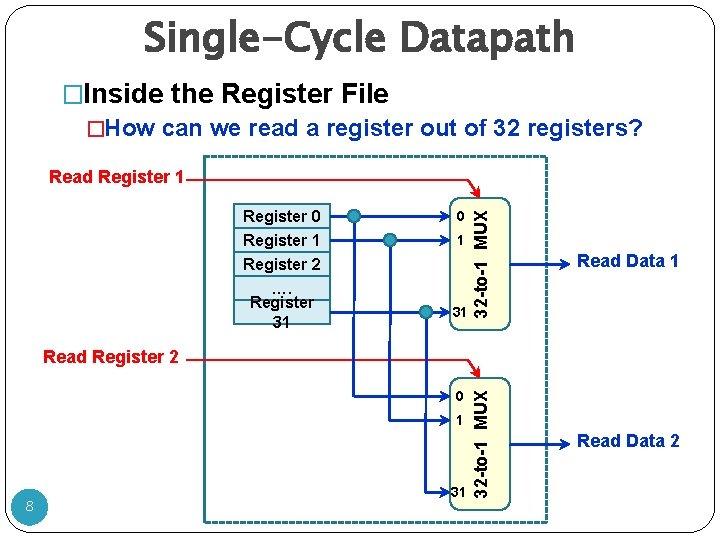
Single-Cycle Datapath �Inside the Register File �How can we read a register out of 32 registers? Register 2 …. Register 31 0 1 31 32 -to-1 MUX Register 0 Register 1 Read Data 1 32 -to-1 MUX Read Register 1 Read Data 2 Read Register 2 0 1 8 31
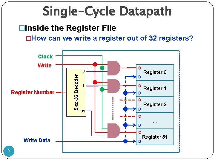
Single-Cycle Datapath �Inside the Register File �How can we write a register out of 32 registers? Clock Write Register Number 5 -to-32 Decoder 0 C D 1 C D C 31 D C Write Data 9 D Register 0 Register 1 Register 2 …. . Register 31
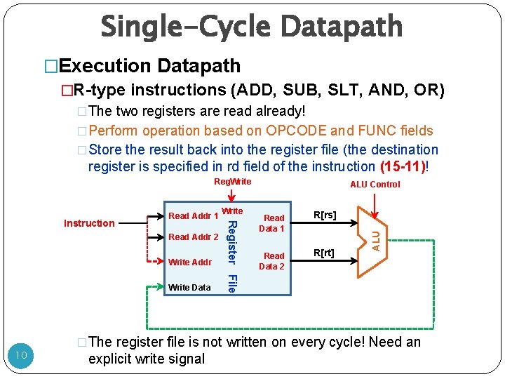
Single-Cycle Datapath �Execution Datapath �R-type instructions (ADD, SUB, SLT, AND, OR) �The two registers are read already! �Perform operation based on OPCODE and FUNC fields �Store the result back into the register file (the destination register is specified in rd field of the instruction (15 -11)! Reg. Write Addr Write Data 10 Read Data 1 Read Data 2 R[rs] R[rt] ALU Read Addr 2 Write Register File Instruction Read Addr 1 ALU Control �The register file is not written on every cycle! Need an explicit write signal
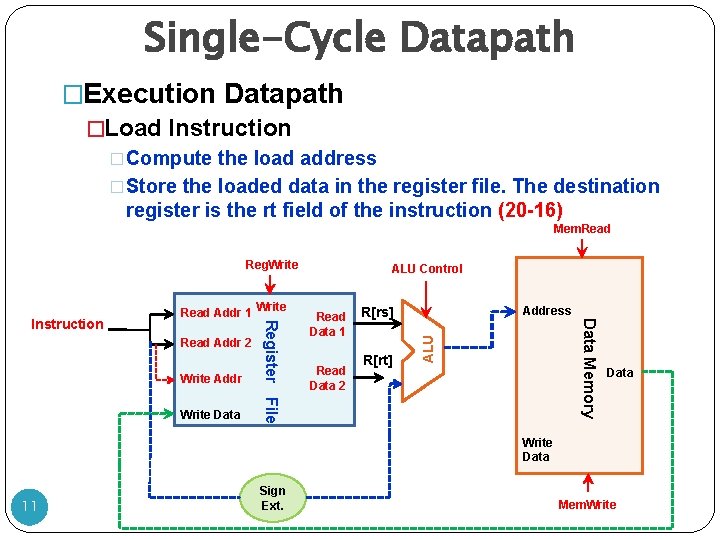
Single-Cycle Datapath �Execution Datapath �Load Instruction �Compute the load address �Store the loaded data in the register file. The destination register is the rt field of the instruction (20 -16) Mem. Read Reg. Write Addr Write Data Read Data 2 R[rs] R[rt] Address ALU Read Data 1 Data Memory Read Addr 2 Write Register File Instruction Read Addr 1 ALU Control Data Write Data 11 Sign Ext. Mem. Write
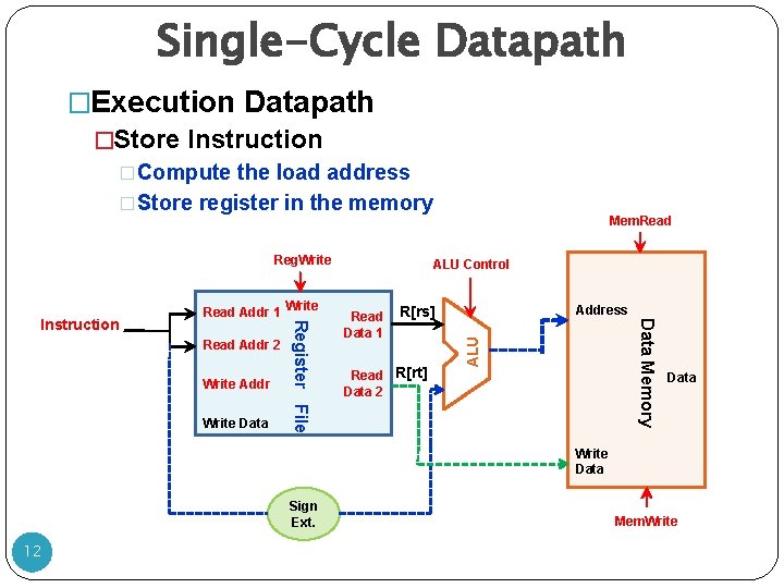
Single-Cycle Datapath �Execution Datapath �Store Instruction �Compute the load address �Store register in the memory Reg. Write Addr Write Data ALU Control R[rs] Read R[rt] Data 2 Address ALU Read Data 1 Data Memory Read Addr 2 Write Register File Instruction Read Addr 1 Mem. Read Data Write Data Sign Ext. 12 Mem. Write
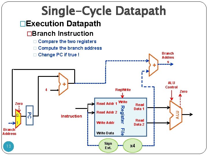
Single-Cycle Datapath �Execution Datapath �Branch Instruction � Compare the two registers � Compute the branch address � Change PC if true ! + ALU Control + Reg. Write 1 Branch Address 13 PC 0 Read Addr 1 Instruction Read Addr 2 Write Addr Write Data Sign Ext. Write Register File Zero Read Data 1 Read Data 2 x 4 ALU 4 Branch Addres s
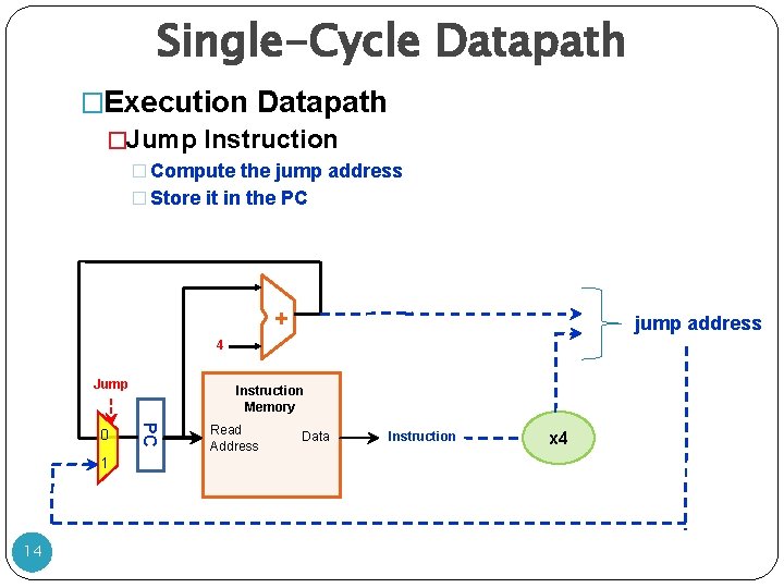
Single-Cycle Datapath �Execution Datapath �Jump Instruction � Compute the jump address � Store it in the PC + jump address 4 Jump 1 14 PC 0 Instruction Memory Read Address Data Instruction x 4
Single-Cycle Datapath �Creating the Single Datapath �Assemble the datapath segments and add control lines and multiplexors as needed �Single cycle design �Fetch, decode and execute each instructions in one clock cycle �No datapath resource can be used more than once per instruction, so some must be duplicated (e. g. , separate Instruction Memory and Data Memory, several adders) �Multiplexors needed at the input of shared elements with control lines to do the selection �Write signals to control writing to the Register File and Data Memory �Cycle time is determined by length of the longest path 15
![Single-Cycle Datapath 1 Instr[25 -0] Shift left 2 PC[31 -28] + 4 0 Jump Single-Cycle Datapath 1 Instr[25 -0] Shift left 2 PC[31 -28] + 4 0 Jump](http://slidetodoc.com/presentation_image_h2/07f710879b3fc8336e7888f9a60ab835/image-16.jpg)
Single-Cycle Datapath 1 Instr[25 -0] Shift left 2 PC[31 -28] + 4 0 Jump Branch ALUOp Instr[31 -26] Read Instr[31 -0] Address Memto. Reg Mem. Write ALUSrc Reg. Write ovf Read Addr 1 Register Read Instr[20 -16] Read Addr 2 Data 1 File 0 Write Addr Read 1 Instr[15 -11] Write Data zero 0 Data 2 Sign 16 Extend ALU 1 Instr[15 -0] 16 PCSrc Mem. Read Instr[25 -21] PC 1 Control Unit Reg. Dst Instruction Memory + Shift left 2 0 32 Instr[5 -0] ALU control Address Data Memory Read Data 1 Write Data 0
Single-Cycle Control � Need to design the control that generates the appropriate control signals based on the Opcode and Function fields to � Specify the operation of the ALU � Control the data flow by selecting the appropriate input of the multiplexors � With the following observations across different instructions � Op field is always in bits 31 -26 of the instruction � Address of registers to be read are always specified by � The rs field (bits 25 -21) � The rt field (bits 20 -16) � For LW and SW, the rs field is the base register � Address of register to be written is in one of two places � For LW, the address is the rt field (bits 20 -16 ) � For R-type, the address is the rd field (bits 15 -11) 17 � Offset for BEQ, LW, and SW is always in bits 15 -0 of the instruction
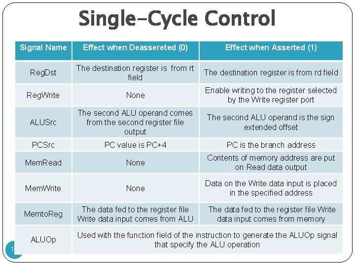
Single-Cycle Control 18 Signal Name Effect when Deassereted (0) Effect when Asserted (1) Reg. Dst The destination register is from rt field The destination register is from rd field Reg. Write None Enable writing to the register selected by the Write register port ALUSrc The second ALU operand comes from the second register file output The second ALU operand is the sign extended offset PCSrc PC value is PC+4 PC is the branch address Mem. Read None Contents of memory address are put on Read data output Mem. Write None Data on the Write data input is placed in the specified address Memto. Reg The data fed to the register file Write data input comes from ALU The data fed to the register file Write data input comes from memory ALUOp Used with the function field of the instruction to generate the ALUOp signal that specify the ALU operation
![R-type Instruction Data/Control Flow 1 Instr[26 -0] Shift left 2 PC[31 -28] + 4 R-type Instruction Data/Control Flow 1 Instr[26 -0] Shift left 2 PC[31 -28] + 4](http://slidetodoc.com/presentation_image_h2/07f710879b3fc8336e7888f9a60ab835/image-19.jpg)
R-type Instruction Data/Control Flow 1 Instr[26 -0] Shift left 2 PC[31 -28] + 4 0 Jump Branch ALUOp Instr[31 -26] Read Instr[31 -0] Address Memto. Reg Mem. Write ALUSrc Reg. Write ovf Read Addr 1 Register Read Instr[20 -16] Read Addr 2 Data 1 File 0 Write Addr Read 1 Instr[15 -11] Write Data zero 0 Data 2 Sign 16 Extend ALU 1 Instr[15 -0] 19 PCSrc Mem. Read Instr[25 -21] PC 1 Control Unit Reg. Dst Instruction Memory + Shift left 2 0 32 Instr[5 -0] ALU control Address Data Memory Read Data 1 Write Data 0
![Load Word Instruction Data/Control Flow 1 Instr[26 -0] Shift left 2 PC[31 -28] + Load Word Instruction Data/Control Flow 1 Instr[26 -0] Shift left 2 PC[31 -28] +](http://slidetodoc.com/presentation_image_h2/07f710879b3fc8336e7888f9a60ab835/image-20.jpg)
Load Word Instruction Data/Control Flow 1 Instr[26 -0] Shift left 2 PC[31 -28] + 4 0 Jump Branch ALUOp Instr[31 -26] Read Instr[31 -0] Address Memto. Reg Mem. Write ALUSrc Reg. Write ovf Read Addr 1 Register Read Instr[20 -16] Read Addr 2 Data 1 File 0 Write Addr Read 1 Instr[15 -11] Write Data zero 0 Data 2 Sign 16 Extend ALU 1 Instr[15 -0] 20 PCSrc Mem. Read Instr[25 -21] PC 1 Control Unit Reg. Dst Instruction Memory + Shift left 2 0 32 Instr[5 -0] ALU control Address Data Memory Read Data 1 Write Data 0
![Branch Equal Instruction Data/Control Flow 1 Instr[26 -0] Shift left 2 PC[31 -28] + Branch Equal Instruction Data/Control Flow 1 Instr[26 -0] Shift left 2 PC[31 -28] +](http://slidetodoc.com/presentation_image_h2/07f710879b3fc8336e7888f9a60ab835/image-21.jpg)
Branch Equal Instruction Data/Control Flow 1 Instr[26 -0] Shift left 2 PC[31 -28] + 4 0 Jump Branch ALUOp Instr[31 -26] Read Instr[31 -0] Address Memto. Reg Mem. Write ALUSrc Reg. Write ovf Read Addr 1 Register Read Instr[20 -16] Read Addr 2 Data 1 File 0 Write Addr Read 1 Instr[15 -11] Write Data zero 0 Data 2 Sign 16 Extend ALU 1 Instr[15 -0] 21 PCSrc Mem. Read Instr[25 -21] PC 1 Control Unit Reg. Dst Instruction Memory + Shift left 2 0 32 Instr[5 -0] ALU control Address Data Memory Read Data 1 Write Data 0
![Jump Instruction Data/Control Flow 1 Instr[26 -0] Shift left 2 PC[31 -28] + 4 Jump Instruction Data/Control Flow 1 Instr[26 -0] Shift left 2 PC[31 -28] + 4](http://slidetodoc.com/presentation_image_h2/07f710879b3fc8336e7888f9a60ab835/image-22.jpg)
Jump Instruction Data/Control Flow 1 Instr[26 -0] Shift left 2 PC[31 -28] + 4 0 Jump Branch ALUOp Instr[31 -26] Read Instr[31 -0] Address Memto. Reg Mem. Write ALUSrc Reg. Write ovf Read Addr 1 Register Read Instr[20 -16] Read Addr 2 Data 1 File 0 Write Addr Read 1 Instr[15 -11] Write Data zero 0 Data 2 Sign 16 Extend ALU 1 Instr[15 -0] 22 PCSrc Mem. Read Instr[25 -21] PC 1 Control Unit Reg. Dst Instruction Memory + Shift left 2 0 32 Instr[5 -0] ALU control Address Data Memory Read Data 1 Write Data 0
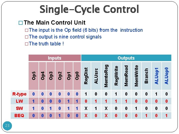
Single-Cycle Control � The Main Control Unit �The input is the Op field (6 bits) from the instruction �The output is nine control signals �The truth table ! 23 Op 4 Op 3 Op 2 Op 1 Op 0 Reg. Dist ALUsrc Memto. Reg. Write Mem. Read Mem. Write Branch ALUop 1 ALUop 0 Outputs Op 5 Inputs R-type 0 0 0 1 0 LW 1 0 0 0 1 1 1 1 0 0 SW 1 0 1 1 X 0 0 1 0 0 0 BEQ 0 0 0 1 0 0 X 0 0 0 1
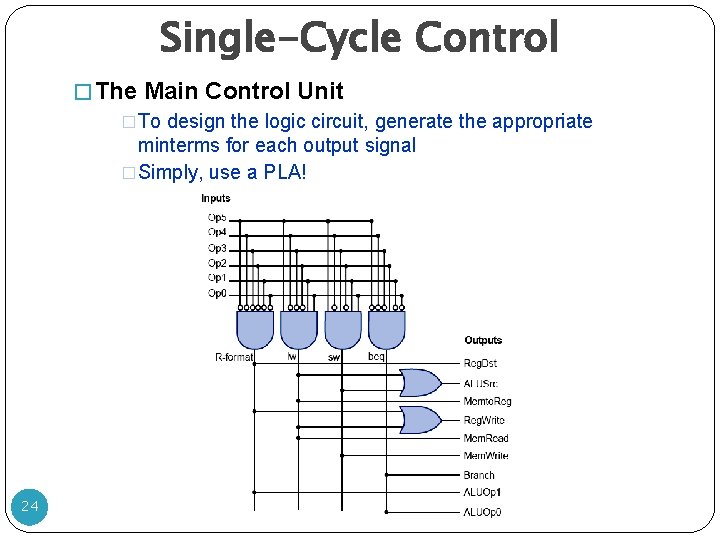
Single-Cycle Control � The Main Control Unit �To design the logic circuit, generate the appropriate minterms for each output signal �Simply, use a PLA! 24
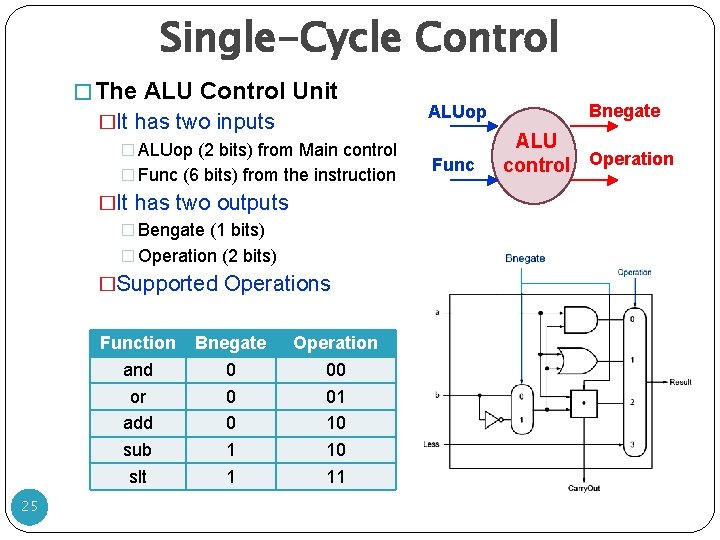
Single-Cycle Control � The ALU Control Unit �It has two inputs � ALUop (2 bits) from Main control � Func (6 bits) from the instruction �It has two outputs � Bengate (1 bits) � Operation (2 bits) �Supported Operations Function and or add sub slt 25 Bnegate 0 0 0 1 1 Operation 00 01 10 10 11 ALUop Func Bnegate ALU control Operation
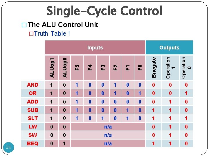
Single-Cycle Control � The ALU Control Unit �Truth Table ! ALUop 0 F 5 F 4 F 3 F 2 F 1 F 0 Bnegate Operation 1 Operation 0 26 Outputs ALUop 1 Inputs AND 1 0 0 0 OR 1 0 1 0 0 1 ADD 1 0 0 0 0 1 0 SUB 1 0 0 0 1 1 0 SLT 1 0 1 0 1 1 1 LW 0 0 n/a 0 1 0 SW 0 0 n/a 0 1 0 BEQ 0 1 n/a 1 1 0
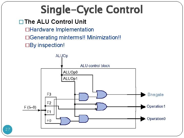
Single-Cycle Control � The ALU Control Unit �Hardware Implementation �Generating minterms!! Minimization!! �By inspection! 27
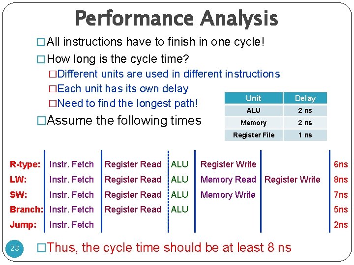
Performance Analysis � All instructions have to finish in one cycle! � How long is the cycle time? �Different units are used in different instructions �Each unit has its own delay �Need to find the longest path! �Assume the following times Unit Delay ALU 2 ns Memory 2 ns Register File 1 ns R-type: Instr. Fetch Register Read ALU Register Write 6 ns LW: Instr. Fetch Register Read ALU Memory Read Register Write 8 ns SW: Instr. Fetch Register Read ALU Memory Write 7 ns Branch: Instr. Fetch Register Read ALU Jump: 28 Instr. Fetch �Thus, the cycle time should be at least 8 ns 5 ns 2 ns
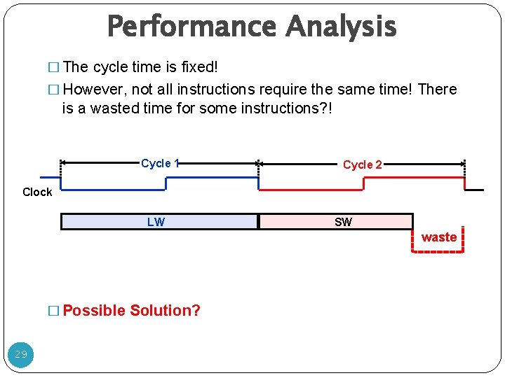
Performance Analysis � The cycle time is fixed! � However, not all instructions require the same time! There is a wasted time for some instructions? ! Cycle 1 Cycle 2 Clock LW SW waste � Possible Solution? 29
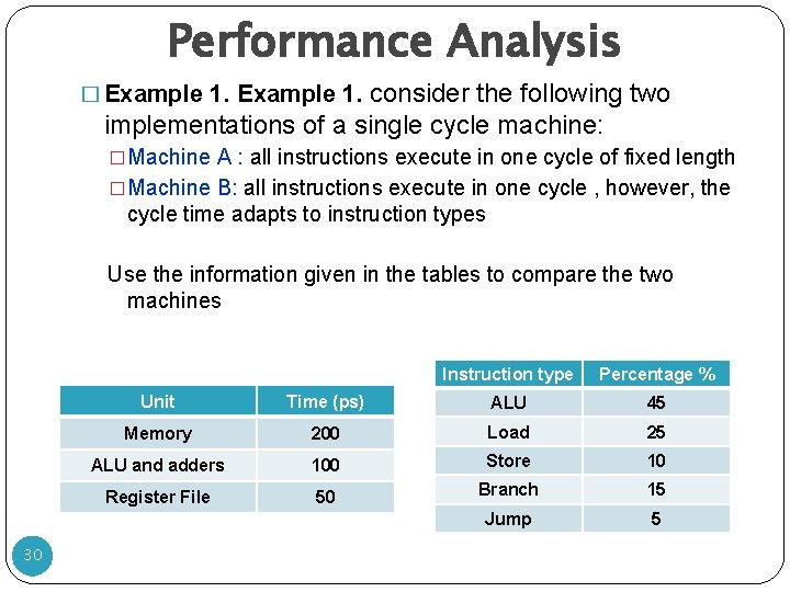
Performance Analysis consider the following two implementations of a single cycle machine: � Example 1. �Machine A : all instructions execute in one cycle of fixed length �Machine B: all instructions execute in one cycle , however, the cycle time adapts to instruction types Use the information given in the tables to compare the two machines 30 Instruction type Percentage % Unit Time (ps) ALU 45 Memory 200 Load 25 ALU and adders 100 Store 10 Register File 50 Branch 15 Jump 5
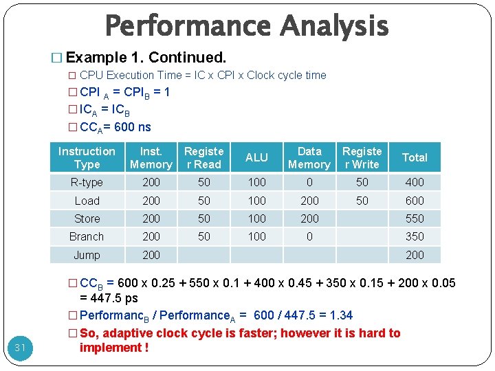
Performance Analysis � Example 1. Continued. � CPU Execution Time = IC x CPI x Clock cycle time � CPI = CPIB = 1 � ICA = ICB � CCA= 600 ns A Instruction Type Inst. Memory Registe r Read ALU Data Memory Registe r Write Total R-type 200 50 100 0 50 400 Load 200 50 100 200 50 600 Store 200 50 100 200 550 Branch 200 50 100 0 350 Jump 200 � CCB = 600 x 0. 25 + 550 x 0. 1 + 400 x 0. 45 + 350 x 0. 15 + 200 x 0. 05 31 = 447. 5 ps � Performanc. B / Performance. A = 600 / 447. 5 = 1. 34 � So, adaptive clock cycle is faster; however it is hard to implement !
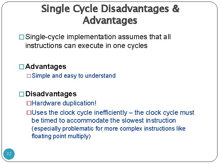
Single Cycle Disadvantages & Advantages � Single-cycle implementation assumes that all instructions can execute in one cycles � Advantages �Simple and easy to understand � Disadvantages �Hardware duplication! �Uses the clock cycle inefficiently – the clock cycle must be timed to accommodate the slowest instruction (especially problematic for more complex instructions like floating point multiply) 32
- Slides: 32