Basic Equations for Device Operation Transport equations The

Basic Equations for Device Operation Transport equations: The total e- and hole current densities are the sum of the drift due to electric field, e and diffusion due to concentration gradient components: (1) (2) where Jn and Jp are e- and hole current densities, respectively n and p are e- and hole concentrations, respectively mn and mp are e- and hole mobilities, respectively. The total current density is given by: J = Jn + Jp S. Saha Page 1
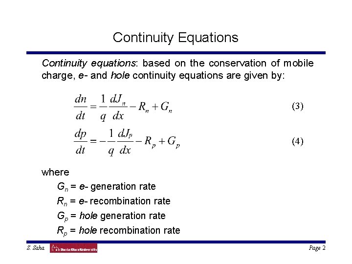
Continuity Equations Continuity equations: based on the conservation of mobile charge, e- and hole continuity equations are given by: (3) (4) where Gn = e- generation rate Rn = e- recombination rate Gp = hole generation rate Rp = hole recombination rate S. Saha Page 2

Poisson’s Equation Poisson’s equation: (5) where e = electric field r(x) = space charge density (charge/cm 3) K = dielectric constant eo = permittivity of free space = 8. 854 x 10 -14 F/cm (6) S. Saha Page 3

Poisson’s Equation Another form of Poisson’s Equation (Gauss’s Law): (7) where QS = integrated charge density In silicon, r consists of: mobile charges: e- and holes with concentrations n and p, respectively. fixed charges: ionized acceptors and donors with concentrations Na- and Nd+, respectively. (8) S. Saha Page 4

Carrier Concentration - Boltzmann’s Relations (9) (10) S. Saha Page 5

Carrier Concentration (11) (12) (13) S. Saha Page 6
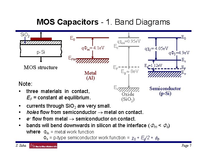
MOS Capacitors - 1. Band Diagrams Si. O 2 E 0 qcox=0. 95 e. V q. Fm= 4. 1 e. V p-Si E 0 Ec qc. S= 4. 05 e. V EFM MOS structure Metal (Al) Note: • three materials in contact, EF = constant at equilibrium. • • EF Eg » 8 e. V Ev Oxide (Si. O 2) q. FS=4. 9 e. V Ec Eg=1. 12 e. V EF Ev Semiconductor (p-Si) currents through Si. O 2 are very small. holes flow from semiconductor ® metal on contact. e- flow from metal ® semiconductor on contact. bands will bend downwards in silicon at the interface (Fm < Fs) where Fm = metal work function Fs = p-type semiconductor work function = c. S + Eg/2 + f. B. S. Saha Page 7

MOS Capacitor at Equilibrium: Applied V = 0 Ec 0. 4 e. V 3. 10 e. V 3. 15 e. V Ec EF • Abrupt transition in Ec and Ev levels at the material interfaces. • For Fm < Fs, band bends downward. • A typical potential drop ~ 0. 4 e. V across Si. O 2. This depends on EF in Si. This potential can be supported because no current flows through Si. O 2. • Substantial barriers exist to current flow from: Ev 3. 8 e. V Ev Al Si. O 2 p-Si S ® M (~ 3. 10 e. V) M ® S (~ 3. 15 e. V). • Depletion region exists near the surface because EF near the surface is further from Ev than the bulk region. • An applied voltage, DVfb = Fm - Fs = Fms can make the band flat. S. Saha Page 8

MOS Capacitor - Flat Band, V = Vfb • EF is constant in Si because Si. O 2 prevents any current flow (i. e. , Si is at equilibrium). • Ec and Ev are flat. • hole concentration is uniform in Si and Si. O 2 (as shown by flat Ec and Ev). Þ FLAT-BAND. • S. Saha The voltage required to achieve flat band condition is Vfb = fms. Page 9

MOS Capacitor – Accumulation, V < Vf. B EFM Ec EF Ev q. V - ve Al Si. O 2 p-Si • EF is still constant in the Si since Si. O 2 prevents any current flow. • EF is closer to Ev at the surface. more holes accumulated near the surface than the bulk. Þ ACCUMULATION. S. Saha Page 10

MOS Capacitor – Depletion, V > VFB f. B EFM q. V Ec Ei EF Ev + ve Al Qg Si. O 2 p-Si Qd • EF is still constant in Si (I = 0). • EF is farther from Ev at the surface. The surface is depleted of holes. Þ DEPLETION. S. Saha Page 11

MOS Capacitor – Inversion, V >> VFB f. B Ys • • EF is still constant in Si (I = 0). EF is closer to Ec at the surface than it is to Ev. more e- than holes at the surface. • • If Ys = 0, the surface becomes intrinsic • If fs > - f. B, the surface will have an e- concentration > hole concentration in the bulk Þ STRONG INVERSION. S. Saha If 0 < Ys < - f. B, the surface will become slightly n-type: Þ WEAK INVERSION. Page 12
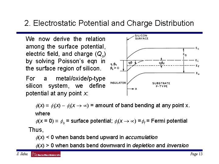
2. Electrostatic Potential and Charge Distribution We now derive the relation among the surface potential, electric field, and charge (Qs) by solving Poisson’s eqn in the surface region of silicon. For a metal/oxide/p-type silicon system, we define potential at any point x: f(x) º fi(x) - fi(x ® µ) = amount of band bending at any point x. where f(x = 0) º fs = surface potential; fi(x ® µ) =ff = Fermi potential Thus, f(x) < 0 when bands bend upward in accumulation f(x) > 0 when bands bend downward in depletion and inversion S. Saha Page 13

Band Bending (14) (15) (16) S. Saha Page 14

Band Bending Thus, the charge density at a depth x in the substrate is given by: (17) Substituting n(x), p(x), Na, and Nd in Poisson’s equation we can determine surface charge density in silicon substrate. (18) S. Saha Page 15
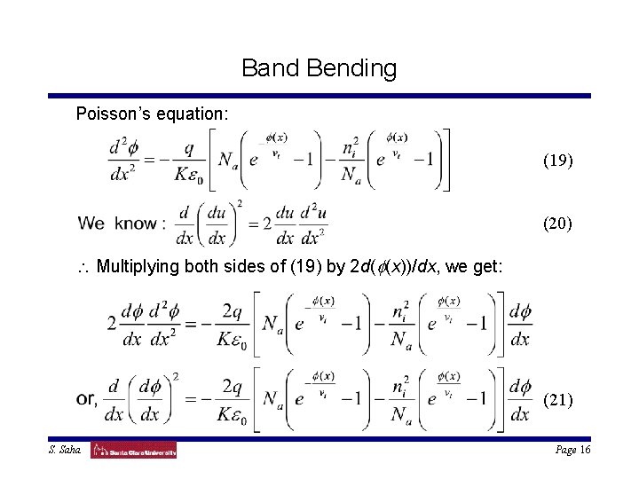
Band Bending Poisson’s equation: (19) (20) Multiplying both sides of (19) by 2 d(f(x))/dx, we get: (21) S. Saha Page 16

Band Bending Integrate from the bulk (f = 0, df/dx = 0) toward the surface at any point x to get: (22) (23) At x = 0, f = fs and E = Es, then from Gauss’s law (7), the total charge per unit area induced in silicon (equal and opposite to the charge on the metal gate is: Qs = - Ke 0 Es S. Saha Page 17
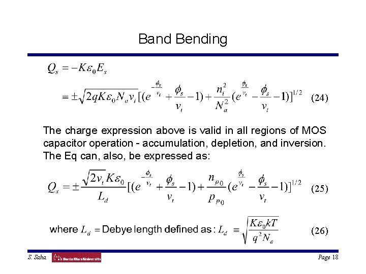
Band Bending (24) The charge expression above is valid in all regions of MOS capacitor operation - accumulation, depletion, and inversion. The Eq can, also, be expressed as: (25) (26) S. Saha Page 18
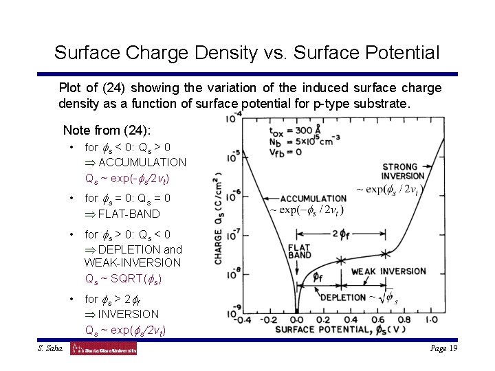
Surface Charge Density vs. Surface Potential Plot of (24) showing the variation of the induced surface charge density as a function of surface potential for p-type substrate. Note from (24): • for fs < 0: Qs > 0 Þ ACCUMULATION Qs ~ exp(-fs/2 vt) • for fs = 0: Qs = 0 Þ FLAT-BAND • for fs > 0: Qs < 0 Þ DEPLETION and WEAK-INVERSION Qs ~ SQRT(fs) • for fs > 2 ff Þ INVERSION Qs ~ exp(fs/2 vt) S. Saha Page 19
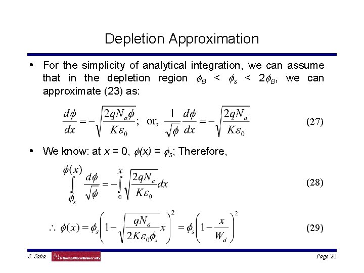
Depletion Approximation • For the simplicity of analytical integration, we can assume that in the depletion region f. B < fs < 2 f. B, we can approximate (23) as: (27) • We know: at x = 0, f(x) = fs; Therefore, (28) (29) S. Saha Page 20

Depletion Approximation (30) • (29) is a parabolic Eq with the vertex at f(x) = 0, x = Wd. Thus, Wd = distance to which band-bending extends = width of the depletion region. • Then the depletion layer charge density is given by: (31) • In an MOS system, Wd reaches a maximum, Wd, max at the onset of inversion defined by fs º 2 f. B = (2 k. T/q)ln(Na/ni). (32) S. Saha Page 21
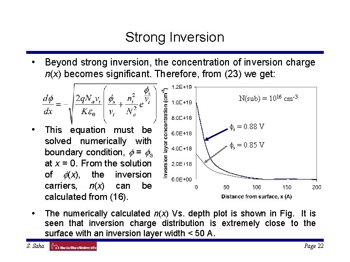
Strong Inversion • Beyond strong inversion, the concentration of inversion charge n(x) becomes significant. Therefore, from (23) we get: N(sub) = 1016 cm-3 • This equation must be solved numerically with boundary condition, f = fs at x = 0. From the solution of f(x), the inversion carriers, n(x) can be calculated from (16). • S. Saha fs = 0. 88 V fs = 0. 85 V The numerically calculated n(x) Vs. depth plot is shown in Fig. It is seen that inversion charge distribution is extremely close to the surface with an inversion layer width < 50 A. Page 22
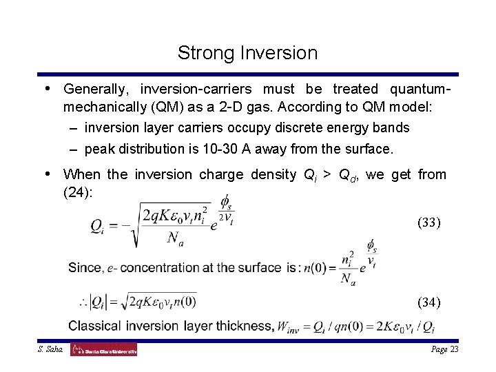
Strong Inversion • Generally, inversion-carriers must be treated quantummechanically (QM) as a 2 -D gas. According to QM model: – inversion layer carriers occupy discrete energy bands – peak distribution is 10 -30 A away from the surface. • When the inversion charge density Qi > Qd, we get from (24): (33) (34) S. Saha Page 23

3. Low Frequency C – V Characteristics Assuming silicon at equilibrium. The total capacitance of an MOS structure is: C = d(-Qs)/d. Vg where the applied gate bias, Vg of an MOS system is: Vg = Vfb + Vox + fs or, d. Vg = d. Vox + dfs where Vox = voltage drop in the oxide (35) Thus, the total capacitance equals the oxide capacitance, Cox and the silicon capacitance, Cs connected in series. S. Saha Page 24

Low Frequency C – V Characteristics From (24), we get: (36) From (36), we can calculate C - V characteristics in different regions of MOS operation. S. Saha Page 25
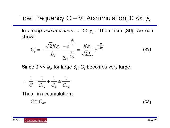
Low Frequency C – V: Accumulation, 0 << fs In strong accumulation, 0 << fs. Then from (36), we can show: (37) Since 0 << fs, for large fs, Cs becomes very large. (38) S. Saha Page 26
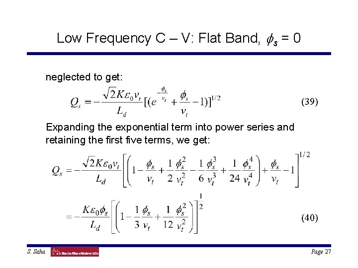
Low Frequency C – V: Flat Band, fs = 0 neglected to get: (39) Expanding the exponential term into power series and retaining the first five terms, we get: (40) S. Saha Page 27
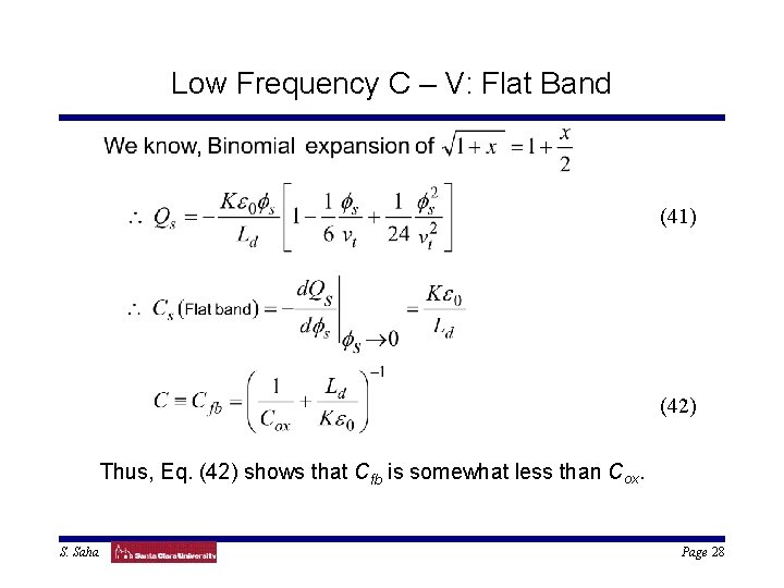
Low Frequency C – V: Flat Band (41) (42) Thus, Eq. (42) shows that Cfb is somewhat less than Cox. S. Saha Page 28

Low Frequency C – V: Depletion, f. B < fs < - f. B In depletion, the general expression for Cd is given by (36). However, we can derive an approximate expression from depletion approximation using Eq. (30) and (31). We know that: (43) Thus, C decreases with the increase in Vg S. Saha Page 29
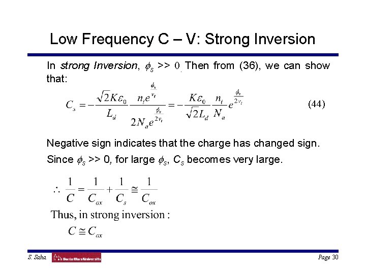
Low Frequency C – V: Strong Inversion In strong Inversion, fs >> 0. Then from (36), we can show that: (44) Negative sign indicates that the charge has changed sign. Since fs >> 0, for large fs, Cs becomes very large. S. Saha Page 30
4. Intermediate and High Frequency C - V • There are plenty of majority carriers which can respond to the A. C. signal. • The minority carriers, on the other hand, are scarce and have to originate from: – diffusion from bulk substrate – generation in the depletion region – external sources (e. g. n+ diffusion region etc. ) • Thus, the inversion charge can not respond to the applied A. C. signal higher than 100 Hz. • Therefore, at any high frequency applied signal to Vg: § § S. Saha Qi is assumed to be constant Q d = Cs Page 31
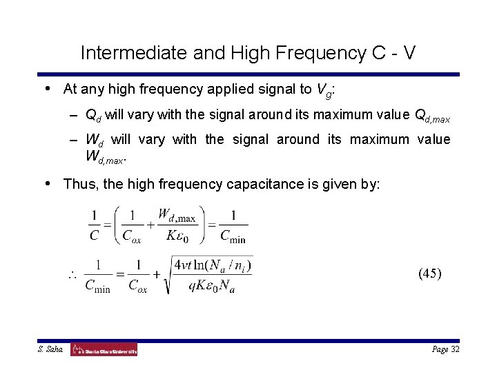
Intermediate and High Frequency C - V • At any high frequency applied signal to Vg: – Qd will vary with the signal around its maximum value Qd, max – Wd will vary with the signal around its maximum value Wd, max. • Thus, the high frequency capacitance is given by: (45) S. Saha Page 32
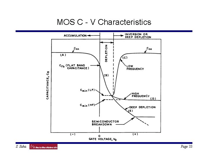
MOS C - V Characteristics S. Saha Page 33
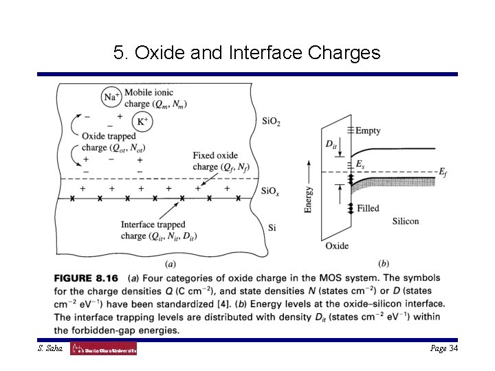
5. Oxide and Interface Charges S. Saha Page 34

5. Oxide and Interface Charges • Types of origins: – fixed interface charge, Qf: believed to be uncompensated Si -Si bonds, on the order of +1010 cm-2. – interface trapped-charge, Qit: due to un-terminated Si bonds, on the order of 1010 cm-2. – Oxide trapped-charge, Qot: due to defects in the Si. O 2 network, usually negligible in advanced MOSFET devices. Can be guaranteed after a large amount of charges have passed through the Si. O 2 and broken up the network. – mobile charge, Qm: sue to alkaline ions (e. g. , Na, K), usually very low concentration (~ 109 cm-2) in advanced technology. S. Saha Page 35

Effects of Qf and Qot on C - V • The flat-band voltage change due to Qf and Qot is: (46) • If Qot is small, Qf can be estimated by DVfb. S. Saha Page 36

Effects of Qf and Qot on C - V Figure. S. Saha Page 37

Effects of Qm on C - V By bias-temperature stress, Qm can be moved from Si-Si. O 2 interface to the metal-Si. O 2 interface. The shift in VFB can be used to estimate Qm. Figure. S. Saha Page 38

Effects of Qit on C - V • Interface trapped-charge, Qit: – the traps have energy levels distributed in the band gap – the charge state of the traps depends on Fermi level. thus, as the surface potential is swept from flat band towards depletion, the traps will try to pin the surface potential, i. e. it will take more gate voltage to move the surface potential through the traps. S. Saha Page 39

Effects of Qit on C - V Assume acceptor type traps: (47) Thus, Cs is in parallel with Cit. Hence, the capacitor model is: (48) S. Saha Page 40

6. Polysilicon Gates At equilibrium (Vg = 0). At Inversion (Vg >> 0). Vox f. B Ec Ei EF Ev f. S VG Ec Ei EF fp Ev n+ poly Si. O 2 p-Si Work-function difference: n+poly with p-type Si: f. MS = - Eg/2 - (k. T/q)ln(NA/ni) (49) p+poly with n-type Si: f. MS = Eg/2 + (k. T/q)ln(ND/ni) (50) S. Saha Page 41

Polysilicon Depletion Effect Note: • Capacitance at inversion, Cinv does not return to Cox. • Cinv shows a maximum value, Cmax < Cox. • Cmax as the polysilicon doping concentration, Np . • As Np , depletion width¯ Cmax ® Cox for higher Np. Total capacitance at strong inversion is given by: 1/C = 1/Cox + 1/Csilicon + 1/Cpoly As VG , Csilicon but xd(poly) Þ Cpoly¯. Low frequency C - V shows a local maximum at a certain VG. S. Saha Page 42

7. Inversion Layer Quantization • Typically, near the silicon surface, the inversion layer charges are confined to a potential well formed by: – oxide barrier – bend Si-conduction band at the surface due to the applied gate potential, VG. E 2 E 1 E 0 Bottom of the well E Edge of EC Distance from the surface • Due to the confinement of inversion layer e- (in p-Si): – e- energy levels are grouped in discrete sub-bands of energy, Ej – each Ej corresponds to a quantized level for e- motion in the normal direction. S. Saha Page 43

Inversion Layer Quantization • Due to Quantum Mechanical (QM) effect, the inversion layer concentration: – peaks below the Si. O 2/Si interface - » 0 at the interface determined by the boundary condition of the e- wave function. n (cm-3) Classical QM Depth • Solve Schrodinger and Poisson Eq self-consistently with the boundary conditions for wave function equal to: – 0 for x < 0 in oxide – 0 at x = ¥. S. Saha Page 44

QM Effect on MOS Capacitors • At high fields, Vth since more band bending is required to populate the lowest sub-band, which is some energy above the bottom of EC. • Once the inversion layer forms below the surface, a higher Vg over-drive is required to produce a given level of inversion charge density. That is, the effective gate oxide thickness, t. OXeff by: Dt. OX = (eox/esi)Dz (51) • Inversion layer quantization can be treated as bandgap widening due to an increase in the effective bandgap by DEg given by: (52) Here, DEg = Eg. QM - Eg. CL. (52) Þ ni¯ and n¯ due to QM effect. S. Saha Page 45

Home Work 1: Due 0 ct 6, 2005 1) An MOS capacitor is built with the structure shown below. The capacitor areas over the N and P regions are the same. The threshold voltages for the N and P substrates are -1 and +1 volts respectively. Sketch the shape of the high frequency (1 MHz) C-V curve that you would expect to measure for this structure. Label as many points as possible and explain. Al Si. O 2 N P 2) In practical MOS systems, measurements of C - V sometimes show hysteresis effects; that is, the C - V curves look like the sketch in Fig. The sketch refers to measurements made when VG is swept with a very low frequency triangular wave (~ 1 Hz) and the A. C. measurement frequency is of the order of 1 k. Hz or higher. The sense of the hysteresis on such a curve can be observed experimentally to be either counterclockwise, as shown, or else be clockwise. S. Saha Page 46

Home Work 1: Due Oct 6, 2005 The hysteresis sense allows one to differentiate between the two most common cause of non-ideal behavior. (a) Show this by considering the following non-ideal effects: (i) field-aided movement of positive ions in the insulator and (ii) trapping of free carriers from the channel in traps at the oxide-Si interface Qit. (b) Using qualitative reasoning, prepare a table with sketches of the expected C - V plots for n- and p-type substrates; on each sketch indicate the sense of the hysteresis (i. e. , clockwise or counterclockwise). S. Saha Page 47
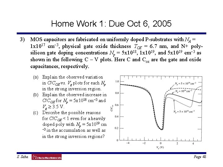
Home Work 1: Due Oct 6, 2005 3) MOS capacitors are fabricated on uniformly doped P-substrates with NA = 1 x 1017 cm-3, physical gate oxide thickness TOX = 6. 7 nm, and N+ polysilicon gate doping concentrations Np = 5 x 10¹⁸, 1 x 10¹⁹, and 5 x 1019 cm-3 as shown in the following C – V plots. Here C and Cox are the gate and oxide capacitances, respectively. (a) Explain the observed variation in C/COX vs. Vg plots for each Np in the strong inversion region. (b) Explain the observed increase in C/COX for Np = 5 x 1018 cm-3 and Vg ³ 3. 5 V. (c) Describe the possible reasons for C/COX < 1 even for a heavily doped poly with Np = 5 x 1019 cm -3 in the accumulation as well as in the strong inversion regions? S. Saha Page 48
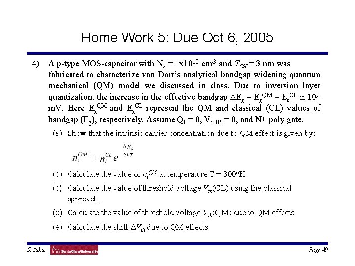
Home Work 5: Due Oct 6, 2005 4) A p-type MOS-capacitor with Na = 1 x 1018 cm-3 and TOX = 3 nm was fabricated to characterize van Dort’s analytical bandgap widening quantum mechanical (QM) model we discussed in class. Due to inversion layer quantization, the increase in the effective bandgap DEg = Eg. QM - Eg. CL @ 104 m. V. Here Eg. QM and Eg. CL represent the QM and classical (CL) values of bandgap (Eg), respectively. Assume Qf = 0, VSUB = 0, and N+ poly gate. (a) Show that the intrinsic carrier concentration due to QM effect is given by: (b) Calculate the value of ni. QM at temperature T = 300 o. K. (c) Calculate the value of threshold voltage Vth(CL) using the classical approach. (d) Calculate the value of threshold voltage Vth(QM) due to QM effects. (e) Calculate the shift DVth due to QM effects. S. Saha Page 49
- Slides: 49