Basic Electronics Engineering 104010 Unit III Number System
")
Basic Electronics Engineering (104010)

Unit III : Number System and Logic Gates � Number System: - ◦ Binary, BCD, Octal, Decimal, Hexadecimal their conversion and arithmetic ◦ De-Morgan’s theorem. � Basic Gates: - ◦ AND, OR, NOT � Universal Gate- ◦ NAND, NOR � Exclusive Gates ◦ XOR, XNOR � Combinational Design ◦ Half adder, Full adder � Flip Flop’s ◦ SR, JK, T and D � Introduction to Microprocessor and Microcontroller ◦ Block diagram and explanation

Number System � Decimal � The number system we are familiar with, used every day, is the decimal number system. � Referred to as the base-10 system. � The base-10 system is a positional system � The base-10 number system has 10 distinct symbols, or digits (0, 1, 2, 3, … 8, 9).

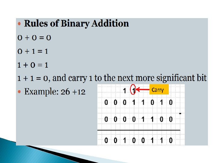
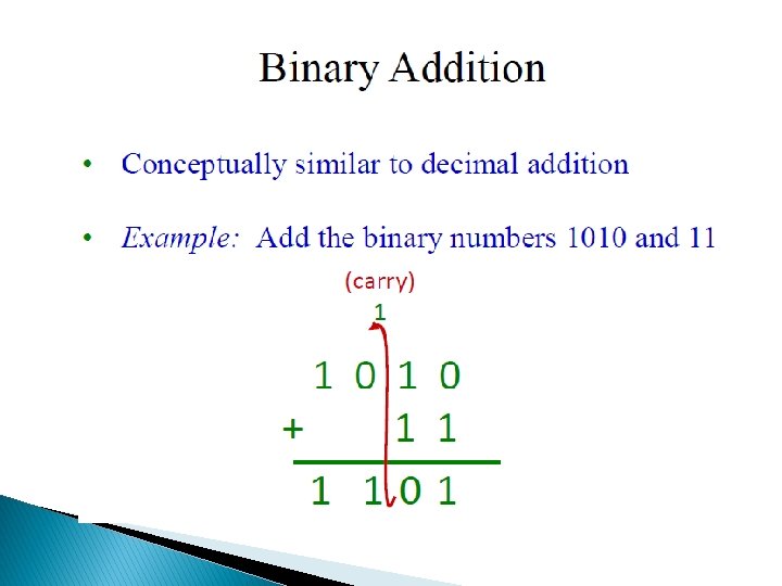
Binary �The point: All data in a computer is represented in binary. A base-2 system, or binary number system. �The term ‘bit’ is a contraction of the words ‘binary’ and ‘digit’, and when talking about binary numbers. �The base-2 system has exactly two symbols: 0 and 1. � 0 and 1 are logical values, not the values of a physical quantity. �A string of eight bits (such as 11000110) is termed a byte. A collection of four bits (such as 1011) is smaller than a byte, and is hence termed a nibble.

BCD Binary-Coded Decimal � � � � � We close with a brief overview of a different manner of converting between binary and decimal. In some practical applications we will use a digital logic circuit to drive a numeric display, where each individual display unit displays a single digit. So, for example, we might have the number 472 in our logic circuit, and we would like to display this on three separate display units (one for the 4, one for the 7 and one for the 2). Working with this sort of display hardware is facilitated through the use of binary-coded decimal (BCD), where each individual digit is represented by a 4 -bit number. For example, to represent the decimal number 472 in binary-coded decimal (BCD), we convert each digit to a four bit binary number, independent of the other decimal digits. Thus, 472 equal 0100 0111 0010 in BCD.

Octal � Octal Numbering System Eight symbols: ◦ 0, 1, 2, 3, 4, 5, 6, 7 • ◦ Notice that we no longer use 8 or 9 Base Comparison: Base 10: 0, 1, 2, 3, 4, 5, 6, 7, 8 , 9, 10, 11, 12… ◦ Base 8: 0, 1, 2, 3, 4, 5, 6, 7, 10 , 11, 12, 13, 14… Example: What is (15)8 in base 10? � (15)8 = ( 1 x 8^1) + ( 5 x 8^ 0) = (13)10 � Example: What is (7061)8 in base 10? �(7061)8 = ( 7 x 8 ^3) + ( 0 x 8^2) + ( 6 x 8^1) + ( 1 x 8^0) � = 36331

Hexadecimal � The base-16 hexadecimal number system has 16 digits (0, 1, 2, 3, 4, 5, 6, 7, 8, 9, A, B, C, D, E and F). � Converting between binary and hexadecimal is exceedingly easy— much easier than converting between binary and decimal

Converting a Decimal Number to a Binary Number: Method 1 � The first method of converting from a decimal number to a binary number entails expressing the decimal number as a sum of powers of 2. � To convert the decimal number x to binary: ◦ Step 1. Find the highest power of two less than or equal to x. The binary representation will have a one in this position. Denote the value of this highest power of 2 as y. ◦ Step 2. Now subtract this power of two (y) from the decimal number (x), denoting the result as z: �Z = x - y. ◦ Step 3. If z = 0, you are done. Otherwise, let x = z and return to Step 1 above.

Converting a Decimal Number to a Binary Number: Method 2 � The second method of converting a decimal number to a binary number entails repeatedly dividing the decimal number by 2, keeping track of the remainder at each step. � To convert the decimal number x to binary: ◦ Step 1. Divide x by 2 to obtain a quotient and remainder. The remainder will be 0 or 1. ◦ Step 2. If the quotient is zero, you are finished: Proceed to Step 3. Otherwise, go back to Step 1, assigning x to be the value of the most-recent quotient from Step 1. ◦ Step 3. The sequence of remainders forms the binary representation of the number. � This method of repeated division by 2 is called the ‘double-dabble’ method.
10 into a Binary number.")
Convert (26)10 into a Binary number.

Converting a Hexadecimal Number to a Decimal Number � Write the hexadecimal number as a sum of powers of 16. � For example, considering the hexadecimal number 1 A 9 B above, we convert this to decimal as: � 1 A 9 B = 1 x 163 + Ax 162+ 9 x 161 +Bx 160 � = 4096 + 10(256) + 9(16) + 11(1) = 6811

Converting a Decimal Number to a Hexadecimal Number � � To convert from decimal to hexadecimal is to use the same division algorithm that you used to convert from decimal to binary, but repeatedly dividing by 16 instead of by 2. As before, we keep track of the remainders, and the sequence of remainders forms the hexadecimal representation. ◦ Convert (348)10 into a hexadecimal number.

Converting a Hexadecimal Number to a Binary Number � We can convert directly from hexadecimal notation to the equivalent binary representation by using the following procedure: ◦ Convert each hexadecimal digit to a four digit binary number, independent of the other hexadecimal digits. ◦ Concatenate the resulting four-bit binary numbers together. ◦ For example, to convert the hexadecimal number 4 DA 9 to binary, we first convert each hexadecimal digit to a four-bit string: � 4 = 0100 D = 1101 A = 1010 9 = 1001 ◦ and then concatenate the results: The resulting binary number is: 0100 1101 1010 1001. ◦ We can drop leading zeros (from the leftmost quartet only!), giving us: � 4 DA 9 = 100110110101001

Converting a Binary Number to a Hexadecimal Number � Convert directly from binary notation to the equivalent hexadecimal � representation by using the following procedure: ◦ Starting at the right, collect the bits in groups of 4 ◦ Convert each group of 4 bits into the equivalent hexadecimal digit ◦ Concatenate the resulting hexadecimal digits ◦ For example, to convert 110110101001 to hexadecimal, we collect the bits into groups of 4 starting at the right: 1101 1010 1001, and then we convert each collection of bits into a hexadecimal digit: ◦ 1101 1010 1001 ◦ DA 9 ◦ Thus 110110101001 = DA 9

Number Representation

De. Morgans Theorem � De Morgan’s most important work are two related theorems that have to do with how NOT gates are used in conjunction with AND and OR gates: ◦ An AND gate with inverted output behaves the same as an OR gate with inverted inputs. ◦ An OR gate with inverted output behaves the same as an AND gate with inverted inputs. ◦ An AND gate with inverted output is also called a NAND gate, of course, and an OR gate with inverted output is also called a NOR gate. � Thus, De Morgan’s laws can also be stated like this: ◦ A NAND gate behaves the same as an OR gate with inverted inputs. ◦ A NOR gate behaves the same as an AND gate with inverted inputs. � � simplification techniques used to simplify Boolean expressions. the simpler the resulting the Boolean expression, the simpler the resulting logic.

De. Morgan’s First Theorem

De. Morgan’s Second Theorem

Example using De. Morgan’s Theorem

Logic Gates � There are seven logic gates: � There are three basic types of digital logic gates � Universal gates � Exclusive Gates ◦ AND, OR, XOR, NOT, NAND, NOR, and XNOR. ◦ AND Gate ◦ OR Gate and ◦ NOT Gate (NOT gates and Buffers are single input devices that can also have a Tri-state High-impedance output which can be used to control the flow of data onto a common data bus wire) ◦ The NAND gate and the NOR gate both are classed as “Universal” gates as they can be used to construct any other gate type. ◦ Any combinational circuit can be constructed using only two or three input NAND or NOR gates. ◦ EX-OR ◦ EX-NOR

AND GATE The AND gate has two or more inputs and one output signal. � This is a gate which performs a logical operation multiplication, which is commonly known as AND function. � This gate is called an AND gate because the gate gives output will be high when all input values are high the output is low or 0 when any of the inputs are low or 0. � The symbol of AND Gate & Truth Table is shown below. �

OR Gate The OR gate has two or more inputs and one output signal. � A logical operation or addition, which is commonly known as OR function. � This gate is called an OR gate because the gate gives output high only if any or all input values are high The output is low or 0 when both the inputs are low or 0. � The symbol of OR Gate & Truth Table is shown below. �

NOT GATE � Single input and a single output � Known as an inverter, because it does the inversion of applied binary signal at the � The symbol of NOT Gate & Truth Table is shown below.

NAND GATE � Has two or more input terminals and one output terminals. � Cascade combination of AND – NOT gates. � The output of NAND gate is high or 1 when any one input is low or 0 and the output is low or 0 when all inputs are high or 1. � The symbol of NAND Gate & Truth Table is shown below.

NOR GATE � Has two or more input terminals and one output terminal. � Cascade combination of OR – NOT gates. � The output of NOR gate is high or 1 when all the inputs are low or 0 and the output is low or 0 when one or all inputs are high or 1. The symbol of NOR Gate & Truth Table is shown below.
 GATE: � This gate has two or more input terminals and")
Exclusive- OR (EX-OR) GATE: � This gate has two or more input terminals and one output terminal. � The EX-OR Gate has the output only high when an odd number of inputs are high and the output is low when both the inputs are low and both the inputs are high. � The symbol of EX-OR Gate & Truth Table is shown below.
 GATE � The EX-NOR gate has terminals like OR gate i.")
Exclusive- NOR (EX-NOR) GATE � The EX-NOR gate has terminals like OR gate i. e, two or more input terminals and one output terminal. � The EX-NOR Gate has the output only high when both the inputs have the same values either high or low and the output is low when an odd number inputs are high. � The symbol of EX-NOR Gate & Truth Table is shown below.

Binary Subtraction

1's And 2's Complement of Binary Number The 1's complement and the 2's complement of binary number are important because they permit the representation of negative numbers.

Binary Subtraction using Two’s Complement Method � Calculation of 2's Complement
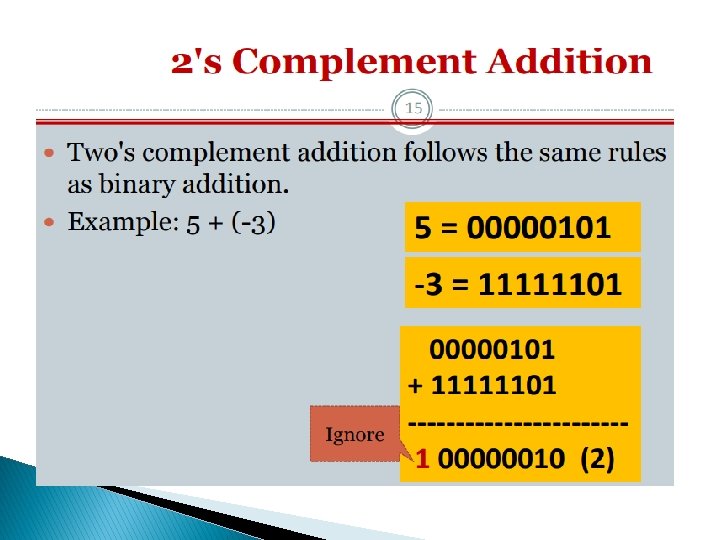
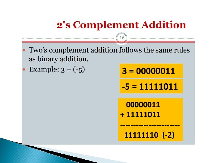

Adding/Subtracting using 2’s Complement

Adders � The most basic operation a computer can perform is to add two numbers together through binary � these types of addition operations are carried out by a special kind of combinational circuit called adders � A combination circuit that performs the addition of two bits is half adder � A adder performs the addition of 2 significant bits and a previous carry is called a full adder

Half Adder � Half Adder: is a combinational circuit that performs the addition of two bits, this circuit needs two binary inputs and two binary outputs.

One-bit Full Adder � � � Full Adder is a combinational circuit that performs the addition of three bits (two significant bits and previous carry). It consists of three inputs and two outputs, two inputs are the bits to be added, the third input represents the carry form the previous position. The full adder is usually a component in a cascade of adders, which add 8, 16, etc, binary numbers. The output is equal to 1 when only one input is equal to 1 or when all three inputs are equal to 1. The output has a carry 1 if two or three inputs are equal to 1.

One-bit Full Adder • The implementation of half adder using exclusive–OR and an AND gates is used to show that two half adders can be used to construct a full adder. • The inputs to the XOR gate are also the inputs to the AND gate.

One-bit Full Adder

Full Adder using Half Adders

Categories of Circuits � With the two general categories of circuits being: ◦ 1. Combinational Circuits where the input values explicitly determine the output ◦ 2. Sequential Circuits where the output is a function of the input values as well as the existing stage of the circuit �a. Thus, sequential circuits usually involve the storage of information

1 -bit Memory Cell: Flip-flops A latch is an electronic logic circuit that has two inputs and one output. � Storse a data value � ◦ non-volatile; will not lose value over time ◦ often incorporated in static memory � Technically a latch is level triggered and a flip-flop is edge triggered (on the clock cycle). ◦ ◦ SR or set–reset latch, which may also be called a SR flip-flop D or data flip-flip T or toggle flip-flop JK flip-flop MEMORY � We know that flip-flop can store either zero or one permanently until a change is made in the inputs. � Flip-flops are the basic technology behind computer memory chips �

S-R Latch � � � Then the SR description stands for “Set-Reset”. This simple flip-flop is basically a one-bit memory bistable device that has two inputs, one which will “SET” the device (meaning the output = “ 1”), and is labelled S and one which will “RESET” the device (meaning the output = “ 0”), labelled R. S-R Latch Acts as a simple memory with two states ◦ The latch - holds (stores) when S = R = 0 ◦ is set (to 1) by bringing S = 1 with R = 0 ◦ is reset (to 0) by bringing R = 1 with S = 0 � � The condition S = R = 1 must be avoided because it leads to an indeterminate condition. This can cause a race condition to occur.

SR Latch with Enable � The S and R inputs only effect the output states when the enable input or timing control C is high. ◦ This controls when the latch responds to its inputs. ◦ The timing control input, commonly called “gate”, or “clock”, or “latch enable”, is used to coordinate when new data can be written into the memory element, and conversely, when data cannot be written ( � � A clock determines when computational activities occur � � Signals determines what computational activities occur ◦ The latch holds (stores) its value while the enable input is low — latches it! ◦ Any changes in the inputs during the time when enable is high will affect the output immediately: the circuit is said to be transparent. ◦ This circuit still has a major problem: the stored value is indeterminate if S = R = 1 when the clock goes low

D Flip-Flop The problem with S = R = 1 can be avoided using a common input D as shown. � It is a variant of the more basic S-R flip-flop (Set-Reset) � The output of the latch now: – � ◦ follows the D input while C = 1 (transparent) ◦ holds its value while C = 0 (Q = last Q when C went low) no matter what happens at the input � This circuit is often called a transparent latch.

D Flip-Flop � It acts as a simple memory or ‘latch’. � The previous value stored, Qn, has no effect, unlike other flip-flops. It therefore acts as a simple memory or ‘latch’. � The most widely used flip-flops: simple to build and design with. � A register comprises several D flip-flops, one for each bit to be stored.

JK Flip-Flop The name JK flip-flop is termed from the inventor Jack Kilby from texas instruments. One of the most useful and versatile flip-flop The fundamental difference of this device is the feedback paths to the AND gates of the input, i. e. Q is AND-ed with K and CP and Q’ with J and CP. 1. if the J and K input are both at 1 and clock is applied then the output will change irrespective of its previous condition. 2. if the J and K input are both at 0 and clock is applied then the output will not change. 3. No indeterminate condition, in the operation of JK flipflop.
 Flip-Flop The T flip-flop is a single input version of the JK")
Toggle (T) Flip-Flop The T flip-flop is a single input version of the JK flip-flop. � The T flip-flop is obtained from the JK type if both inputs are tied together. � The toggle, or T, flip-flop is a bistable device, where the output of the T flip-flop "toggles" with each clock pulse. � Till CP=0, the output is in hold state (three input AND gate principle). � When CP=1, for T=0, previous output is memorized by the circuit. When T=1 along with the clock pulse, the output toggles from the previous value �

Flip-Flop Symbols and Applications � Typical flip-flop symbols, using a “black-box approach”, an approach that is useful to represent specific clusters of electronic components. � There are two general ways in which flip-flops may be interconnected to perform useful functions: counters and registers

Block Diagram of Microprocessor

Block Diagram of Microcontroller

Difference Between Microprocessor and Microcontroller Sr No Microprocessor Microcontroller 1 It is a central processing unit on a single silicon based integrated chip It is a byproduct of a development of a microprocessor 2 It has no Memory, IO Units, Timers and other peripheral on the chips. It has a CPU along with Memory, IO Units, Timers and other peripherals embedded on the single chip. 3 It uses an external bus to It uses an internal controlling bus interface Memory, IO Units, which is not available to the board Timers and other peripherals. designer. 4 It is used for general purpose It is used for application specific applications which are able to systems. data. handle loads of data. 5 It is complex and expensive with large number of It is simple and inexpensive with less number of instructions to

Practicals based on Unit 3 � Test and verify the truth tables of: ◦ a) Basic and Universal Gates (Study the data sheet of respective IC’s) ◦ b) Half / Full Adder ◦ c) RS/JK/T/D flip flop � 74 ls 279/7476/ 7474

Text and Reference Books � “Modern Digital Electronics” by R. P. Jain, 4 th Edition, Tata Mc. Graw Hill � “Digital Fundamentals” by Thomas. L. Floyd, 11 th Edition, Pearson

�Thank You all.
- Slides: 56